Supporting Information
| Supporting Information File 1: STEM image showing a cross-sectional view of an ion-polished Cu sample (30 keV Ga, 3371 ions/nm2). Differences in the milling depth for different grains are visible. | ||
| Format: TIF | Size: 1.5 MB | Download |
| Supporting Information File 2: Ion channeling video showing a Cu sample changing during Ga ion polishing. | ||
| Format: MP4 | Size: 7.4 MB | Download |
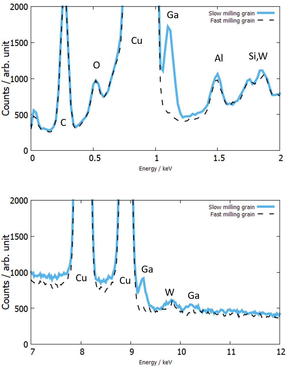
| Supporting Information File 3: Energy-dispersive X-ray point spectra recorded on a slower milling grain and on a faster milling grain of a 30 keV Ga ion-polished Cu sample. A dose of 3371 ions/nm2 was used for the polishing experiment. | ||
| Format: PNG | Size: 268.8 KB | Download |
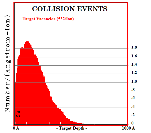
| Supporting Information File 4: SRIM simulation showing vacancies for 25 keV Ne ion irradiation of Cu at a 0° incidence angle. | ||
| Format: BMP | Size: 720.9 KB | Download |
| Supporting Information File 5: STEM image showing the interface of a non-irradiated area and a 30 kV Ga 0° incidence irradiated area. | ||
| Format: TIF | Size: 2.9 MB | Download |
| Supporting Information File 6: SAED patterns of a non-irradiated Cu sample prepared by electropolishing, PIPS, and FIB. In all cases, the SAED pattern matches that of Cu. (a) Electropolishing, the SAED pattern matches the [110] ZA for Cu. The measured d-spacing for d200,A = 0.177 nm is slightly smaller than the reported value of d002,Cu = 0.181 nm for Cu (PDF number 00-004-0836); however, within an acceptable discrepancy for this d-spacing. The measured d-spacing for d11−1,B = 0.209 nm matches the reported value of d111,Cu = 0.209 nm. (b) PIPS, the SAED pattern matches the [310] ZA for Cu. The measured d-spacing for d131,A = 0.209 nm matches the reported value of d111,Cu = 0.209 nm. The measured d-spacing for d200,B = 0.189 nm is slightly larger than the reported value of d002,Cu = 0.181 nm for Cu (PDF number 00-004-0836); however, within an acceptable discrepancy for this d-spacing. (c) FIB-prepared TEM lamella, the SAED pattern matches the [100] ZA for Cu. The measured d-spacing for d022,A = 0.133 nm is in good agreement with the reported value of d022,Cu = 0.128 nm for Cu (PDF number 00-004-0836). The measured d-spacing for d002,B = 0.192 nm is slightly larger than the reported value of d002,Cu = 0.181 nm for Cu (PDF number 00-004-0836), however; within an acceptable discrepancy for this d-spacing. The SAED measurements recorded on all the TEM lamellae which were prepared using different methods are in good agreement, suggesting that the FIB TEM lamella preparation did not significantly alter the TEM measurement results. | ||
| Format: TIF | Size: 4.3 MB | Download |
Cite the Following Article
Is the Ne operation of the helium ion microscope suitable for electron backscatter diffraction sample preparation?
Annalena Wolff
Beilstein J. Nanotechnol. 2021, 12, 965–983.
https://doi.org/10.3762/bjnano.12.73
How to Cite
Wolff, A. Beilstein J. Nanotechnol. 2021, 12, 965–983. doi:10.3762/bjnano.12.73
Download Citation
Citation data can be downloaded as file using the "Download" button or used for copy/paste from the text window
below.
Citation data in RIS format can be imported by all major citation management software, including EndNote,
ProCite, RefWorks, and Zotero.
Presentation Graphic
| Picture with graphical abstract, title and authors for social media postings and presentations. | ||
| Format: PNG | Size: 10.9 MB | Download |
Citations to This Article
Up to 20 of the most recent references are displayed here.
Scholarly Works
- Agag, G. M.; Aranas, C.; Millare, J. C.; de Yro, P. A. N. Investigating the fracture toughness of weld in S355 KT-40 offshore jacket leg using scanning electron microscopy and nanoscale modelling. Welding International 2025, 1–12. doi:10.1080/09507116.2025.2600611
- Koren, B.; Friedman, O.; Maman, N.; Hayun, S.; Ezersky, V.; Golan, Y. Sample preparation induced phase transitions in solution deposited copper selenide thin films. RSC advances 2021, 12, 277–284. doi:10.1039/d1ra07947f