Search results
Search for "electrodeposition" in Full Text gives 70 result(s) in Beilstein Journal of Nanotechnology.
Laser processing in liquids: insights into nanocolloid generation and thin film integration for energy, photonic, and sensing applications
Beilstein J. Nanotechnol. 2025, 16, 1428–1498, doi:10.3762/bjnano.16.104


Enhancing the photoelectrochemical performance of BiOI-derived BiVO4 films by controlled-intensity current electrodeposition
Beilstein J. Nanotechnol. 2025, 16, 1289–1301, doi:10.3762/bjnano.16.94

- Abstract This study investigates the fabrication of BiVO4 photoanodes using a controlled-intensity current electrodeposition method to improve their photoelectrochemical (PEC) performance. The impact of varying the deposition current density and VO(acac)2 concentration was systematically analyzed to
- samples fabricated with lower current density, highlighting the benefits of the optimized electrodeposition conditions for the former. Keywords: BiOI; BiVO4; electrodeposition; photoelectrochemical water splitting; Introduction In the context of the increasing global energy demand, the development of
- produce BiVO4 thin films at high deposition rates; however, this method resulted in irregular grain structures and significant material defects, limiting the PEC performance improvements. Electrodeposition has emerged as a promising low-cost and scalable technique for BiVO4 film fabrication, offering


Morphology and properties of pyrite nanoparticles obtained by pulsed laser ablation in liquid and thin films for photodetection
Beilstein J. Nanotechnol. 2025, 16, 785–805, doi:10.3762/bjnano.16.60

- . reported the synthesis of single-phase FeS2 thin films using a combination of electrochemical and hydrothermal techniques. The electrodeposition was performed in a nonaqueous electrolytic bath consisting of diethylene glycol [24]. Among the deposition techniques, electrophoretic deposition (EPD) is a cost
- techniques; hence, completely different morphologies are reported. Zebarjad et al. reported cauliflower-like blotches developed on the rough surface of nanostructured FeS2 films made via electrodeposition [57]. Nanowires, nanorods, and nanoribbons of 1D single crystalline FeS2 nanostructures with pyrite


Functionalized gold nanoflowers on carbon screen-printed electrodes: an electrochemical platform for biosensing hemagglutinin protein of influenza A H1N1 virus
Beilstein J. Nanotechnol. 2025, 16, 540–550, doi:10.3762/bjnano.16.42

- was coupled to an automated microfluidics system, and no significant decrease of the electrochemical signal was observed. Keywords: charge transfer; cyclic voltammetry; differential pulse voltammetry; electrochemical impedance spectroscopy; electrodeposition; Introduction Viral infections pose a
- protein at clinically relevant concentrations. Scanning electron microscopy Scanning electron microscopy (SEM) analysis was explored to characterize the surface of the electrodes after electrodeposition of gold nanoparticles (Figure 2). Because of the high conductivity of gold, a difference in contrast is
- based on electrodeposition of gold nanoflowers increased the current response of the electrode because of the larger electroactive surface area compared to a CSPE (Figure 3). The CV analysis of the AuNFs/CSPE showed a peak-to-peak separation of 0.37 V. This value is smaller than in the commercial CSPE


Various CVD-grown ZnO nanostructures for nanodevices and interdisciplinary applications
Beilstein J. Nanotechnol. 2024, 15, 1390–1399, doi:10.3762/bjnano.15.112

- ], radio-frequency magnetron sputtering [47], pulsed laser ablation [48], and electrodeposition methods [49]. They have many application potentials in dye-sensitized solar cells [46], self-powered energy-harvesting devices [47], photocatalysts [48], and turbid lenses [50]. It has been suggested that the


Modulated critical currents of spin-transfer torque-induced resistance changes in NiCu/Cu multilayered nanowires
Beilstein J. Nanotechnol. 2024, 15, 360–366, doi:10.3762/bjnano.15.32

- aluminum oxide (AAO) template-assisted electrodeposition has attracted wide interest because of its low cost as well as high flexibility on tailoring the magnetic properties of magnetic systems and thus STT effects [8][9][10][11][12]. Moreover, it enables a larger number of free layers, whose magnetization
- around 1 µm. The electrodeposition of multilayered nanowires was carried out in situ using a three-electrode potentiostat in the pulsed mode [20] at 25 °C. Note that the nanowires were selectively deposited in the pores on the top of the Ti/Au bottom electrodes as shown in Figure 1a. Therefore, most of
- template were contacted with the top electrodes. After a lift-off process, the 3D devices based on the NiCu/Cu multilayered nanowire array were obtained. A typical device structure is shown in Figure 1b,c. The description of the setup and more details of AAO template fabrication, electrodeposition and


Metal-organic framework-based nanomaterials as opto-electrochemical sensors for the detection of antibiotics and hormones: A review
Beilstein J. Nanotechnol. 2023, 14, 631–673, doi:10.3762/bjnano.14.52


Evaluation of electrosynthesized reduced graphene oxide–Ni/Fe/Co-based (oxy)hydroxide catalysts towards the oxygen evolution reaction
Beilstein J. Nanotechnol. 2023, 14, 420–433, doi:10.3762/bjnano.14.34
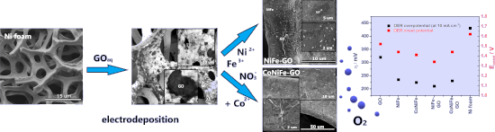
- catalytic activity of the catalysts with and without GO were studied. The catalysts were fabricated via a two-step electrodeposition. The first step included the deposition of GO flakes, which, in the second step, were reduced during the simultaneous deposition of NiFe or CoNiFe. As a result, NiFe-GO and
- catalysts specifically influenced the process. The improvement in the OER by NiFe-GO results mainly from the structure of NiFe and the electroactive surface area of GO. Keywords: electrocatalysts; electrodeposition; energy; hydrogen; oxygen evolution reaction; Introduction Nowadays, the industrial
- influence of the addition of GO to NiFe and CoNiFe oxides/(oxy)hydroxides catalysts towards the OER was studied. NiFe, CoNiFe, NiFe-GO, and CoNiFe-GO were synthesized by electrodeposition directly on nickel foam. The process made it possible to fabricate OER electrodes with reduced GO and without any


Studies of probe tip materials by atomic force microscopy: a review
Beilstein J. Nanotechnol. 2022, 13, 1256–1267, doi:10.3762/bjnano.13.104

- fluoride oxidation at the anode to form nanopores of 50–100 nm in diameter. After electrodeposition, the carbon nanotubes are grown by CVD at 750 °C. If the carbon nanotubes do not grow in a suitable trend, they are removed by oxidation. The CNT tips are then grown again by CVD. The CVD nanotube tips can

Design of surface nanostructures for chirality sensing based on quartz crystal microbalance
Beilstein J. Nanotechnol. 2022, 13, 1201–1219, doi:10.3762/bjnano.13.100

- substances [117]. Various metal or inorganic materials have been explored as chiral selectors in QCM systems based on different strategies and techniques. Sarkar et al. used tartaric acid as a chiral inducer to control the crystalline orientation of CuO films based on the electrodeposition method [118]. The


Biomimetic chitosan with biocomposite nanomaterials for bone tissue repair and regeneration
Beilstein J. Nanotechnol. 2022, 13, 1051–1067, doi:10.3762/bjnano.13.92

- release [110]. Silver and antibiotic drugs were mixed into the biocomposite containing chitosan, graphene oxide, and hydroxyapatite. Furthermore, using one-step electrodeposition, biocomposites were coated on titanium. It has been discovered that the addition of graphene oxide and chitosan improves
Electrocatalytic oxygen reduction activity of AgCoCu oxides on reduced graphene oxide in alkaline media
Beilstein J. Nanotechnol. 2022, 13, 1020–1029, doi:10.3762/bjnano.13.89

- electrodeposition. Among the combinations, the Ag–Cu (3:1) alloy showed the better electrode catalytic activity and the highest onset (0.85 V vs RHE) and half-wave potential (0.76 V vs RHE) with a limiting current density of 4.19 mA·cm−2, along with an electron transfer value of 3.86 in 0.1 M KOH [21]. Linic and co


Comparing the performance of single and multifrequency Kelvin probe force microscopy techniques in air and water
Beilstein J. Nanotechnol. 2022, 13, 922–943, doi:10.3762/bjnano.13.82

- minimizing the required low VAC needed for operation in order to avoid the associated problems, for example, current flow, electrodeposition, or Faradaic reactions [9]. For this assessment, a number of simplifying assumptions have been made: (1) We use a simple spherical model of tip–sample capacitance [2
Influence of thickness and morphology of MoS2 on the performance of counter electrodes in dye-sensitized solar cells
Beilstein J. Nanotechnol. 2022, 13, 528–537, doi:10.3762/bjnano.13.44

- investigated using various techniques such as chemical bath deposition [1], sputtering [2], hydrothermal synthesis [10][11][12][13], wet chemistry [14], thermal reduction [15], and electrodeposition (ED) [20]. Among these methods, ED shows many advances thank to its simplicity and rapidity. Additionally, it
- MoS2/FTO. The resulting DSSCs showed a PCE of 7.16%, similar to that of a Pt/FTO CE (7.48%). The MoS2 film was amorphous and contained agglomerated clusters of nanoparticles [22]. Recently, Gurulakshmi et al. reported on DSSCs using a flexible CE fabricated by electrodeposition of a MoS2 thin film onto
- should be noted that this is the first report dealing with the fabrication of MoS2 honeycomb-like thin films for DSSC application. Results and Discussion Electrodeposition of MoS2 thin films Electrodeposition of MoS2 thin films was carried out from precursor solutions containing a mixture of (NH4)6Mo7O24


Zinc oxide nanostructures for fluorescence and Raman signal enhancement: a review
Beilstein J. Nanotechnol. 2022, 13, 472–490, doi:10.3762/bjnano.13.40

- needed to develop efficient SERS substrates. The combination of several methods including nanosphere lithography, atomic layer deposition, electrodeposition, and electron-beam evaporation resulted in Au-covered hollow urchin-like ZnO structures (Figure 2e–k) [16]. The ZnO layer was deposited on a
- substrate covered with polystyrene spheres by atomic layer deposition, followed by electrodeposition, which was used to grow ZnO nanowires onto the surface. The Au layer was deposited after burning off the polystyrene spheres by electron beam evaporation while monitoring its thickness. Considering the
- morphology for SERS measurements can be fabricated using various methods, including sol–gel synthesis [38], thermal deposition [31][32], chemical vapour deposition [42], or electrodeposition [35], which resulted in 1.2 μm high, vertically aligned nanorods of 60 nm diameter. It was observed that thermal


The effect of metal surface nanomorphology on the output performance of a TENG
Beilstein J. Nanotechnol. 2022, 13, 298–312, doi:10.3762/bjnano.13.25

- concentration, and temperature during the electrodeposition of copper. The samples were characterized using XRD and SEM. The output performance of the TENG is closely related to the size, charge density distribution, and shape of the metal nanoparticles. Keywords: charge density; green energy; metal
- freely. Therefore, there is no high charge density on the tip surface of the polymer surface. Here, size and morphology of nanoscale copper were controlled by adjusting current density, temperature, pH value, and solution concentration during electrodeposition. The effects of different morphologies and
- during electrodeposition. The sample after electrodeposition was dried in a Geruida GRD220H oven. After obtaining 16 groups of experimental samples, PTFE (purchased from Bukraun) was used as the anode, and the experimental sample was used as the cathode to fabricate the TENGs. The open-circuit voltage


Morphology-driven gas sensing by fabricated fractals: A review
Beilstein J. Nanotechnol. 2021, 12, 1187–1208, doi:10.3762/bjnano.12.88

- foam after electrodeposition. Figure 10c and Figure 10d illustrate the porous foam structure formed at 700 °C by thermal oxidation and the dendritic structures formed in pore wall. The foam sensor was able to detect down to 4 ppm of H2S. The highest gas response (S = 576) was obtained for 20 ppm of H2S


Uniform arrays of gold nanoelectrodes with tuneable recess depth
Beilstein J. Nanotechnol. 2021, 12, 957–964, doi:10.3762/bjnano.12.72

- approaches for the preparation of such systems is templated electrodeposition. In the present study, porous anodic alumina templates are used to prepare Au nanoelectrode arrays. Multistage electrodeposition is proposed for the formation of recessed electrodes with the ability to tune the distance between the
- pathways to further improve the recessed nanoelectrode arrays based on anodic alumina templates are discussed. Keywords: anodic alumina; gold; nanoelectrode array; recessed electrode; templated electrodeposition; Introduction A nanoelectrode array (NEA) is a set of regularly arranged isolated metal
- available porous AAO films with a highly irregular structure to prepare the Au nanowell electrodes with 600 nm depth by templated electrodeposition. It is worth noting that the percentage of nanoelectrodes in the array that are involved in electrochemical reactions has not been discussed in detail. At the


The role of deep eutectic solvents and carrageenan in synthesizing biocompatible anisotropic metal nanoparticles
Beilstein J. Nanotechnol. 2021, 12, 924–938, doi:10.3762/bjnano.12.69

- surface coating with nanoparticles through electrodeposition. A general electrodeposition setup consists of three electrodes, that is cathode, anode, and a reference electrode [78]. The solvation property and the conductivity of DESs also play a critical role in determining the physical structure, yield
- whereas network like nanostructures were observed when the synthesis temperature was 90 °C. Apart from nanomaterials, DESs are also being exploited for the electrodeposition of alloys for coating applications. For example, Bernasconi et al. developed a non-aqueous electrolyte using choline chloride and
- ethylene glycol in a molar ratio of 1:2 for electrodeposition of a zinc–nickel alloy to provide corrosion protection [90]. Due to the ever-rising interest in DESs for nanomaterial synthesis, a fundamental understanding regarding interfacial behavior and mass transport, such as ionic adsorption, surface


Recent progress in actuation technologies of micro/nanorobots
Beilstein J. Nanotechnol. 2021, 12, 756–765, doi:10.3762/bjnano.12.59

- -shaped micro/nanorobots in batches by template electrodeposition. Under the action of the ultrasonic field, the robots could achieve velocities up to 200 μm/s. Research has shown that standing ultrasonic waves in the megahertz frequency range can suspend, advance, rotate, arrange, and assemble metal


Seebeck coefficient of silicon nanowire forests doped by thermal diffusion
Beilstein J. Nanotechnol. 2020, 11, 1707–1713, doi:10.3762/bjnano.11.153

- fabricated on the top of a silicon nanowire forest, which can be achieved by copper electrodeposition [18]. 2) The optimum doping concentration of the nanowires for the exploitation of the maximum power factor of silicon [3] needs to be found. Both the Seebeck coefficient and the electrical conductivity
- maintained for the chosen doping time (ten minutes, typically). Then, the chips have been allowed to cool maintaining the nitrogen flux. After doping by thermal diffusion, a contact has been provided on top of the silicon nanowire forest exploiting the copper electrodeposition method described in a previous
- publication [18]. At first, a Cr (for adhesion)/Cu double metal layer has been deposited by thermal evaporation both on top of the nanowires and on the other side of the silicon wafer, that is, at the bottom of the substrate. The Cu layer on the top has been used as a seed for the electrodeposition of copper


Gas-sensing features of nanostructured tellurium thin films
Beilstein J. Nanotechnol. 2020, 11, 1010–1018, doi:10.3762/bjnano.11.85

- galvanic displacement of sacrificial cobalt nanowires were employed [15]. Lastly, to grow one-dimensional nanostructures, either template-free electrodeposition of Te, from an ionic liquid binary mixture [16], or thermal evaporation in a furnace under argon gas flow [17] were strategies utilized. The


Transition from freestanding SnO2 nanowires to laterally aligned nanowires with a simulation-based experimental design
Beilstein J. Nanotechnol. 2020, 11, 843–853, doi:10.3762/bjnano.11.69

- driving force). Similar to dendrite formation in electrodeposition, the growth of freestanding NWs is promoted for high material gradients with distance from the substrate surface [36]. This can be observed for dewetted Au thin films and high incoming material rates. Experiments were performed to


A set of empirical equations describing the observed colours of metal–anodic aluminium oxide–Al nanostructures
Beilstein J. Nanotechnol. 2020, 11, 798–806, doi:10.3762/bjnano.11.64

- a metal after electrodeposition [15]. Human vision is trichromatic, i.e., the retina contains three types of colour receptor cells, also known as cones: a) S cones, short-wavelength cones or blue cones; b) M cones, middle-wavelength cones or green cones and c) L cones, long-wavelength cones or red


Preparation, characterization and photocatalytic performance of heterostructured CuO–ZnO-loaded composite nanofiber membranes
Beilstein J. Nanotechnol. 2020, 11, 631–650, doi:10.3762/bjnano.11.50

- using cathodic co-electrodeposition and observed their photocatalytic performance. Fierro et al. [25] synthesized CuO–ZnO composite catalysts by temperature-programmed reduction and applied them in photocatalytic degradation. Nanocomposites loaded with metal oxide semiconductors have excellent optical


