Search results
Search for "photoemission" in Full Text gives 93 result(s) in Beilstein Journal of Nanotechnology.
Chiral plasmonic nanostructures fabricated with circularly polarized light
Beilstein J. Nanotechnol. 2025, 16, 2245–2264, doi:10.3762/bjnano.16.154

- field. This section will cover the experimental methods for observing the near fields of cPNSs. Advanced techniques, such as near-field scanning optical microscopy (NSOM), cathodoluminescence (CL), electron energy loss spectroscopy (EELS), and photoemission electron microscopy (PEEM), offer spatial
- , the map of the electron emission intensity from achiral AuNRs adopts a chiral geometry, as shown in Figure 8d [72]. PEEM can produce time-resolved data to probe the dynamics of photoemission [134]. In addition to EELS and PEEM, the so-called photon-induced near-field electron microscopy (PINEM


Ambient pressure XPS at MAX IV
Beilstein J. Nanotechnol. 2025, 16, 1677–1694, doi:10.3762/bjnano.16.118

- spectrometry will enable a more holistic understanding of structure–function relationships at working interfaces. Additionally, the development of correlated, spatially resolved measurements, potentially via photoemission electron microscopy (PEEM) or scanning probe methods, could further bridge the gap


Enhancing the therapeutical potential of metalloantibiotics using nano-based delivery systems
Beilstein J. Nanotechnol. 2025, 16, 1350–1366, doi:10.3762/bjnano.16.98

- higher light absorption, and greater photoemission output, resulting in enhanced bactericidal activity against S. aureus (Figure 7). The Ir-complex liposomes interact efficiently with 450 nm LED light, leading to ROS generation and subsequent bacterial inactivation at the site of an infected chronic skin


Insights into the electronic and atomic structures of cerium oxide-based ultrathin films and nanostructures using high-brilliance light sources
Beilstein J. Nanotechnol. 2025, 16, 860–871, doi:10.3762/bjnano.16.65

- understanding of cerium oxide-based systems was introduced by the application of resonant photoemission to selectively probe valence band features related to Ce4+ and Ce3+ ions. This can be done by tuning the photon energy at specific resonances related to Ce 4d→Ce 4f0 (Ce4+) and Ce 4d→Ce 4f1 (Ce3+) electronic
- photoemission, as compared to non-resonant photoemission. Synchrotron radiation-based resonant photoemission has facilitated an accurate determination of the dependence of Ce3+ concentration on dimensionality [23]. The technique has also provided an accurate description of the charge transfer processes and
- of surface C or CO [38]. Resonant photoemission detected by a spectroscopic photoemission and low-energy electron microscope (SPLEEM) was also used to acquire local information on the oxidation degree of cerium in mixed zirconia–ceria nanostructures supported on a Rh(111) single crystal [39]. Figure


Changes of structural, magnetic and spectroscopic properties of microencapsulated iron sucrose nanoparticles in saline
Beilstein J. Nanotechnol. 2025, 16, 762–784, doi:10.3762/bjnano.16.59


Thickness dependent oxidation in CrCl3: a scanning X-ray photoemission and Kelvin probe microscopies study
Beilstein J. Nanotechnol. 2025, 16, 749–761, doi:10.3762/bjnano.16.58

- showed that oxygen adsorption on cleaved surfaces facilitates the formation of a stable structure with charge transfer signatures, as identified by high-resolution photoemission spectroscopy [8]. It remains unclear whether similar effects occur in exfoliated thin flakes. Like in other materials, the
- effect) [19][20][21]. A well-known and suitable technique to investigate the electronic structure of surfaces is X-ray photoemission spectro-microscopy [22][6]; in order to obtain the necessary spatial resolution, the beam size must be reduced to tens of nanometers. The Electron Spectroscopy for Chemical
- be suitable for increasing the sensitivity to a number of defects per unit volume forming at the surface, which can be recorded by the significant photoemission core level binding energy shift [25][26]. The significance of these studies lies in the exploration of novel materials with improved


Nanostructured materials characterized by scanning photoelectron spectromicroscopy
Beilstein J. Nanotechnol. 2025, 16, 700–710, doi:10.3762/bjnano.16.54

- reprinted from [13], J. Phys. Chem. Solids, vol. 160, by A. I. Merentsov; A. S. Shkvarin; M. S. Postnikov; L. Gregoratti; M. Amati; P. Zeller; P. Moras; A. N. Titov, “Studying the heterogeneity of the CrxTi1-xCh2 (Ch = S, Se) single crystals using X-ray scanning photoemission microscopy“, article no. 110309


High-temperature epitaxial growth of tantalum nitride thin films on MgO: structural evolution and potential for SQUID applications
Beilstein J. Nanotechnol. 2025, 16, 690–699, doi:10.3762/bjnano.16.53

- still present (33.8 atom % O), along with tantalum oxynitride. Shi et al. [16] synthesized TaN nanocrystals and reported that the TaN 4f7/2 XPS peak appears at 23.5 eV. Similarly, Bayer and collaborators [17] identified the TaC 4f7/2 XPS peak at 23.3 eV, and Yang et al. [18] reported a photoemission


Pulsed laser in liquid grafting of gold nanoparticle–carbon support composites
Beilstein J. Nanotechnol. 2025, 16, 349–361, doi:10.3762/bjnano.16.26

- ][23]. Element-specific relative sensitivity factors resulting from photoemission cross sections and analyzer transmission of photoelectrons were used to determine atom percentages [22]. The measured O 1s atom percentages for each component were used to constrain the respective C 1s peak fits. The


Unveiling the nature of atomic defects in graphene on a metal surface
Beilstein J. Nanotechnol. 2024, 15, 416–425, doi:10.3762/bjnano.15.37

- from STS experiments [49][50][51], it is lower than the energy observed in photoemission experiments [52]. A possible rationale is the locally lifted graphene in the presence of the tip [53], which in turn decreases the charge transfer from graphene to the metal and reduces the p-doping [52] and


Properties of tin oxide films grown by atomic layer deposition from tin tetraiodide and ozone
Beilstein J. Nanotechnol. 2023, 14, 1085–1092, doi:10.3762/bjnano.14.89

- distances average to less sharp XAS peaks. Because of the somewhat less shallow probe depth of XAS recorded in TEY mode (ca. 10 nm) compared to the high surface sensitivity of the recorded photoemission spectra (a few atomic layers) [41] we suggest that less completely oxidised species appear below the


Evaluation of electrosynthesized reduced graphene oxide–Ni/Fe/Co-based (oxy)hydroxide catalysts towards the oxygen evolution reaction
Beilstein J. Nanotechnol. 2023, 14, 420–433, doi:10.3762/bjnano.14.34
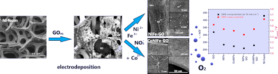
- probably inhibited the electrodeposition process of NiFe and CoNiFe on its surface. This may be the reason for the slower stabilization of the synthesis current density observed in the chronoamperograms (Figure 1a). X-ray diffraction, X-ray photoemission spectroscopy and X-ray absorption spectroscopy
- were conducted using Cu Kα radiation (λ = 1.5404 Å) with a Philips X’Pert Pro diffractometer in the 2θ range from 5° to 35°. The selected 2θ range was selected based on the previous measurements corresponding to similar types of materials [25]. X-ray photoemission spectra (XPS) of the catalysts were


Self-assembly of C60 on a ZnTPP/Fe(001)–p(1 × 1)O substrate: observation of a quasi-freestanding C60 monolayer
Beilstein J. Nanotechnol. 2022, 13, 857–864, doi:10.3762/bjnano.13.76

- tunneling microscopy/spectroscopy and ultraviolet photoemission spectroscopy. C60 nucleates compact and well-ordered hexagonal domains on top of the ZnTPP buffer layer, suggesting a high surface diffusivity of C60 and a weak coupling between the overlayer and the substrate. Accordingly, work function
- fullerene films stabilized directly on metal surfaces. Our results unveil a model system that could be useful in applications in which a quasi-freestanding monolayer of C60 interfaced with a metallic electrode is required. Keywords: fullerene; scanning tunneling microscopy; ultraviolet photoemission
- to this system, new features appear. The photoemission signal from the underlying ZnTPP layer, albeit affected by the screening action of C60 (implying a rather large surface sensitivity of the technique, as also shown in [55] on a similar system), is still detected in those spectral regions not


A nonenzymatic reduced graphene oxide-based nanosensor for parathion
Beilstein J. Nanotechnol. 2022, 13, 730–744, doi:10.3762/bjnano.13.65

- spectra of the samples were recorded in the 1000–3500 cm−1 region with a resolution of 1 cm−1 using a Renishaw via a Reflex micro-Raman spectrometer with an argon ion (514.6 nm) laser. The X-ray photoemission spectroscopy (XPS) data were obtained from a PHI 5000 Versa probe II scanning XPS microprobe


Investigation of a memory effect in a Au/(Ti–Cu)Ox-gradient thin film/TiAlV structure
Beilstein J. Nanotechnol. 2022, 13, 265–273, doi:10.3762/bjnano.13.21

- the relationship [51][52]: where hν = 21.22 eV is the He (I) photon energy, W = 16.01 eV is the width of the spectrum, that is, the energy difference between the VBM and the photoemission cutoff energy, and Eg = 2.80 eV is the bandgap energy calculated from the transmission spectrum. The work function
- (Wf) was determined to be equal to 4.01 eV and was calculated as the difference between the photon energy of the He (I) line and the position of the cutoff energy of the photoemission (17.21 eV). Cross-sectional analysis The structural investigations included measurements of the material composition


Influence of magnetic domain walls on all-optical magnetic toggle switching in a ferrimagnetic GdFe film
Beilstein J. Nanotechnol. 2022, 13, 74–81, doi:10.3762/bjnano.13.5

- deterministic toggle switching. Keywords: all-optical magnetic switching; GdFe; laser-induced domain-wall motion; magnetic domain imaging; photoemission electron microscopy; Introduction The reversal of magnetization at the fastest possible time scales and microscopic length scales is one of the most
- individual ultrashort focused laser pulses has been reported [21]. In this paper, we investigate nondeterministic all-optical toggle switching of a Gd26Fe74 film with out-of-plane easy axis of magnetization by magnetic imaging using photoemission electron microscopy (PEEM) with X-ray magnetic circular
- Information File 1 for temperature-dependent magnetization loops. Magnetic domains were resolved using the photoemission electron microscope (PEEM) at the UE49-PGM SPEEM beamline of BESSY II. The acceleration potential between the sample and the first objective lens of the PEEM was set to 15 keV. X-ray


Interface interaction of transition metal phthalocyanines with strontium titanate (100)
Beilstein J. Nanotechnol. 2021, 12, 485–496, doi:10.3762/bjnano.12.39

- transfer with the oxide substrate was observed, involving both the macrocycle and the central metal atom. For molecules of the first monolayer, an electron transfer to the central metal atom is concluded from transition metal 2p core level photoemission spectra. The number of interacting molecules in the
- resublimed before usage. The materials were evaporated from temperature-controlled crucibles. The nominal layer thickness was estimated from substrate- and adsorbate-related XPS intensity ratios using photoemission cross sections from Yeh and Lindau [41]. A nominal monolayer of lying molecules corresponds to
- (368.2 eV), and Au 4f7/2 (84.0 eV). For X-ray photoelectron diffraction measurements, the angular acceptance of the analyzer was set to ±4°. Angular distribution curves were measured for the Sr 3d, Ti 2p, and O 1s photoemission peaks at two azimuths ([100] and [110], determined by LEED); the step width


Free and partially encapsulated manganese ferrite nanoparticles in multiwall carbon nanotubes
Beilstein J. Nanotechnol. 2020, 11, 1891–1904, doi:10.3762/bjnano.11.170

- attributed to the attachment of manganese ferrite nanoparticles outside the tubes, which is detected by a significant decrease in the σ band emission of the ultraviolet photoemission spectroscopy signal. This is followed by an increase in the density of states at the Fermi level of the attached manganese
- values was estimated to be equal to ±0.1 eV. Due to the charging effect of the oxides, electron flooding was carried out for charge compensation. A helium lamp with 21.2 eV (He I) excitation energy was used for ultraviolet photoemission spectroscopy (UPS, Omicron Nanotechnology). A −5 V sample bias was
- peak is localized at 641.2 eV, with components at 641.0, 642.4, and 644.6 eV. The observed binding energies are reported for the Mn2+ 2p3/2 peak [24] and multiplet constituents [23] (Figure 8d). Hence, it could be inferred that manganese is present in the Mn2+ state. Three photoemission peaks


The influence of an interfacial hBN layer on the fluorescence of an organic molecule
Beilstein J. Nanotechnol. 2020, 11, 1663–1684, doi:10.3762/bjnano.11.149

- states and the dynamical CT in the excited state can be probed by photoemission spectroscopy (PES). In particular, core hole clock spectroscopy has been used to measure the time constant of dynamical CT in the valence band states as a function of the lifetime of the core hole, which is typically of the


Controlling the electronic and physical coupling on dielectric thin films
Beilstein J. Nanotechnol. 2020, 11, 1492–1503, doi:10.3762/bjnano.11.132

- photoemission tomography (PT) have enabled the quantification of both the charge on individual molecules and the number of charged molecules in the 5A monolayer (ML) [14]. For 5A MLs on regularly grown epitaxial MgO(100) films, all molecules appear to be charged. Orbital-resolved STM reveals the LUMO both above
- charge transfer, as evidenced by the absence of an emission from the LUMO in photoemission tomography [21]. This implies that the van der Waals interaction with the metal is sufficient to planarize the molecule. From the STM images shown here of 6P on the MgO(100)/Ag(100) films it is not possible to
- molecules on the surface. The images of orbitals of molecules adsorbed on surfaces can also be obtained from the angular intensity distribution in valence band photoemission experiments via PT [27]. When the photoelectron emission angle is converted to momentum, the resulting momentum maps approximately


Impact of fluorination on interface energetics and growth of pentacene on Ag(111)
Beilstein J. Nanotechnol. 2020, 11, 1361–1370, doi:10.3762/bjnano.11.120

- attributed to the carbon atoms bound to the substrate (C–Ag) belonged to the broken C–F bonds due to the dehalogenation reaction [63][68]. The symmetric F 1s peak was centered at 687.47 eV BE. Figure 1 shows the photoelectron yield (Yp), i.e., the photoemission intensity of the core-levels as a function of
- the screening effect (also often called the mirror force effect), which is commonly observed in photoemission data of organic thin films on metal substrates [71][72][73]. The absence of nonrigid shifts of the core level peaks between the mono- and multilayer coverage, which usually occur in the case


Scanning tunneling microscopy and spectroscopy of rubrene on clean and graphene-covered metal surfaces
Beilstein J. Nanotechnol. 2020, 11, 1157–1167, doi:10.3762/bjnano.11.100

- this peak to the LUMO or LUMO+1. Much wider unoccupied molecular resonances have been observed, too, in pump–probe photoemission experiments on thin C42H28 films adsorbed on highly oriented pyrolithic graphite and traced to the elevated molecule–substrate hybridization with a concomitant reduced


Monolayers of MoS2 on Ag(111) as decoupling layers for organic molecules: resolution of electronic and vibronic states of TCNQ
Beilstein J. Nanotechnol. 2020, 11, 1062–1071, doi:10.3762/bjnano.11.91

- conduction bands between the MoS2 bands on Ag and Au. In a very simple interpretation, this agrees with the lower work function of Ag than that of Au. A down-shift of the conduction band structure by approx. 280 meV has been observed by photoemission of WS2 on Au(111) and Ag(111) [33]. Angle-resolved


Size effects of graphene nanoplatelets on the properties of high-density polyethylene nanocomposites: morphological, thermal, electrical, and mechanical characterization
Beilstein J. Nanotechnol. 2020, 11, 167–179, doi:10.3762/bjnano.11.14

- to the existence of delocalized π electrons (conduction electrons) available for shake-up events following core electron photoemission (Thermo Fisher Scientific Avantage Data System 5.9904; Thermo Fisher XPS: Knowledge Base). In Table 1, the deconvolution fit for the C 1s and O 1s signals is also


Deterministic placement of ultra-bright near-infrared color centers in arrays of silicon carbide micropillars
Beilstein J. Nanotechnol. 2019, 10, 2383–2395, doi:10.3762/bjnano.10.229

- isotopically pure SiC to δB ≈ 10nT/√Hz [51][52]. By increasing the photoemission collection efficiency (C) of the color centers and the number of emitters (N), as for example in micropillars, the magnetic field sensitivity can be dramatically improved to reach magnetic sensing resolution of δB ≈ 10nT/√(C·N·Hz


