Abstract
A simple to implement model is presented to extract interface trap density of graphene field effect transistors. The presence of interface trap states detrimentally affects the device drain current–gate voltage relationship Ids–Vgs. At the moment, there is no analytical method available to extract the interface trap distribution of metal-oxide-graphene field effect transistor (MOGFET) devices. The model presented here extracts the interface trap distribution of MOGFET devices making use of available experimental capacitance–gate voltage Ctot–Vgs data and a basic set of equations used to define the device physics of MOGFET devices. The model was used to extract the interface trap distribution of 2 experimental devices. Device parameters calculated using the extracted interface trap distribution from the model, including surface potential, interface trap charge and interface trap capacitance compared very well with their respective experimental counterparts. The model enables accurate calculation of the surface potential affected by trap charge. Other models ignore the effect of trap charge and only calculate the ideal surface potential. Such ideal surface potential when used in a surface potential based drain current model will result in an inaccurate prediction of the drain current. Accurate calculation of surface potential that can later be used in drain current model is highlighted as a major advantage of the model.
Introduction
Graphene has recently attracted a lot of attention. Its 2D nature along with its significantly high carrier mobility (≈15,000 cm2/(V·s)) make it an ideal material to replace silicon [1] in the more than Moore era. During deposition of the dielectric layer on graphene as well as from deposition of graphene on the substrate defects may be formed in the film resulting in the presence of trap states; Dit states (cm−2·eV−1) at the interface between the dielectric layer and graphene channel [2,3]. These trap states trap mobile carriers degrading the gate field modulation effect, thereby resulting in degraded surface potential.
Popular metal-oxide-graphene field-effect transistor (MOGFET) models do not take into account the detrimental effect of Dit states on device surface potential [4,5]. Zebrev et al. [6], recently presented a model that takes into account the effect of Dit states on the device current. A similar approach has been used by [7]. However, Zebrev’s drain current expression is based on the assumption of presence of constant Dit states over the entire energy range of operation of the device. The assumption does not work generally; recently, significantly varying Dit distribution has been reported for metal-oxide-graphene (MOG) capacitors [8]. This suggests the need for a model that can analytically calculate the interface trap density of MOGFET devices that could later be used in drain current Ids models for efficient Ids performance prediction.
This work presents a method to extract interface trap density of MOGFET with the help of device Ctot–Vgs data. Basic equations and parameters needed to extract interface trap density are explained below. Extraction and verification of extracted trap density is explained following the section below.
Basic equations and parameters
Basic equations
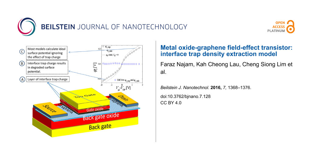
Figure 1a shows the schematic of a typical MOGFET. The channel consists of monolayer graphene with length L deposited on a SiO2 layer with a p-type doped silicon substrate as the backgate (only top-gated monolayer MOGFET is considered in this work). The gate stack consists of a dielectric layer with thickness tox and a metal gate. Qit in Figure 1a refers to the interface trap charge found at the dielectric/channel interface. Figure 1b shows the equivalent capacitive circuit of the typical capacitances in the MOGFET device. In a MOGFET top gate capacitance Cox is in series with the parallel combination of interface trap capacitance Cit which originates from the presence of Dit states, and Cq the quantum capacitance.
![[2190-4286-7-128-1]](/bjnano/content/figures/2190-4286-7-128-1.png?scale=2.0&max-width=1024&background=FFFFFF)
Figure 1: (a) Schematic of MOGFET device. (b) Equivalent capacitive circuit of typical capacitances in MOGFET.
Figure 1: (a) Schematic of MOGFET device. (b) Equivalent capacitive circuit of typical capacitances in MOGFET....
Cq is a graphene material property and is given by [9],
![[2190-4286-7-128-i1]](/bjnano/content/inline/2190-4286-7-128-i1.svg?max-width=590&scale=1.18182)
where, q is the charge on an electron, φs is surface potential,
![[Graphic 1]](/bjnano/content/inline/2190-4286-7-128-i12.svg?max-width=637&scale=1.18182)
![[Graphic 2]](/bjnano/content/inline/2190-4286-7-128-i13.svg?max-width=637&scale=1.18182) is the Planck’s constant, vf is the fermi velocity (1 × 108 cm2/(V·s)), Cqi is a fitting factor independent of φs, and accounts for the finite Cq observed at Dirac point (DP) (at which the fermi level Ef = qφs = 0 = ED, where ED is the energy (eV) at DP).
is the Planck’s constant, vf is the fermi velocity (1 × 108 cm2/(V·s)), Cqi is a fitting factor independent of φs, and accounts for the finite Cq observed at Dirac point (DP) (at which the fermi level Ef = qφs = 0 = ED, where ED is the energy (eV) at DP).
The total capacitance Ctot of MOGFET is given by,
![[2190-4286-7-128-i2]](/bjnano/content/inline/2190-4286-7-128-i2.svg?max-width=590&scale=1.18182)
Applying the capacitor divider relation to Figure 1b, the surface potential φs of MOGFET is given by,
![[2190-4286-7-128-i3]](/bjnano/content/inline/2190-4286-7-128-i3.svg?max-width=590&scale=1.18182)
where Vgs is the gate voltage, VDP is the gate voltage at DP known to be caused by the gate-metal/graphene workfunction difference [10], and/or interface trap states [11], and Vc is the channel voltage drop due to the applied drain bias Vds with Vc = 0 at the source end and Vc = Vds at the drain end.
Solving self-consistently for φs in Equation 3 and Cq = (βgqφs), φs is given by Equation 4,
![[2190-4286-7-128-i4]](/bjnano/content/inline/2190-4286-7-128-i4.svg?max-width=590&scale=1.18182)
Here, the positive (negative) sign applies when (Vgs − VDP − Vc) Cox > 0 (< 0). The sum of Cq + Cit in Equation 2 and Equation 3 can be labeled as Cx. The next few paragraphs explain the procedure for extraction of experimental φs, Cq, Cit and Qit parameters of two sample MOGFET devices which are then used in extraction of their Dit distributions explained in the section “Extraction of interface trap states”.
Experimental φs, Cit, and Qit extraction
Surface potential φs and Cit were extracted for two MOGFET devices using experimental Ctot–Vgs data (from herein referred as Ctot_exp) taken from Device 1 [7], and device 2 [12] (with back-gate bias = 0 V, and Vds = 0). The extracted φs and Cit parameters obtained using experimental Ctot_exp data will be referred to as φs_exp and Cit_exp. The device parameters for both the devices are mentioned in Table 1.
As mentioned in [12] for Device 2, the DC method used to find Cox involves a large amount of ambiguity due to imprecise evaluation of the back-gate capacitance [13], and consequently Cox. A Cox value of 1.00 μF/cm2 along with available Cq and Cit parameters from [12] in Equation 2 was found to reproduce available Ctot_exp, and Cq results very well, instead of the reported value of 0.76 μF/cm2, the former is used instead in this work. The extraction procedure is described next.
Cx can be found from Equation 5 which is derived from manipulating Equation 2. Here Ctot is the respective experimental Ctot–Vgs data for the two experimental devices and Cox is their oxide capacitances mentioned in Table 1.
![[2190-4286-7-128-i5]](/bjnano/content/inline/2190-4286-7-128-i5.svg?max-width=590&scale=1.18182)
Cx obtained from the above equation is then substituted in Equation 3 to extract device’s φs as a function of Vgs, with all the other parameters in Equation 3 known. The extracted φs is referred to as φs_exp as device’s surface potential extracted from experimental Ctot–Vgs data.
Once φs_exp is obtained, Cq can be calculated from Equation 1. Finally, device’s Cit can be obtained using the expression below. The extracted Cit is referred to as Cit_exp as device’s interface trap capacitance obtained from experimental Ctot–Vgs data.
![[2190-4286-7-128-i6]](/bjnano/content/inline/2190-4286-7-128-i6.svg?max-width=590&scale=1.18182)
By substituting Cit_exp in the expression given below, device’s Qit can be extracted.
![[2190-4286-7-128-i7]](/bjnano/content/inline/2190-4286-7-128-i7.svg?max-width=590&scale=1.18182)
In Equation 7 Ef = φs_exp. The extracted Qit is referred to as Qit_exp as the interface trap charge extracted from experimental Ctot–Vgs data.
The relationship between Cit and Qit is given by
![[2190-4286-7-128-i8]](/bjnano/content/inline/2190-4286-7-128-i8.svg?max-width=590&scale=1.18182)
Extraction of interface trap states
For the extraction, according to standard convention [6] acceptor and donor type traps states were considered for the n-type MOGFET, and p-type MOGFET operation, respectively.
The interface trap charge for both acceptor type and donor type trap states can be calculated from the following [11],
![[2190-4286-7-128-i9]](/bjnano/content/inline/2190-4286-7-128-i9.svg?max-width=590&scale=1.18182)
![[2190-4286-7-128-i10]](/bjnano/content/inline/2190-4286-7-128-i10.svg?max-width=590&scale=1.18182)
![[2190-4286-7-128-i11]](/bjnano/content/inline/2190-4286-7-128-i11.svg?max-width=590&scale=1.18182)
Here, in Equation 9–11, Qit_calc denotes the calculated interface trap charge, FtA (FtD) denotes the probability of occupation of k acceptor (donor) type trap states, and EtA (EtD) denotes the ith energy level of each of these k acceptor (donor) type trap state. Dit is the interface trap density defined at the ith energy level. Qit can be found by the integral of product of all the k trap states with their respective FtA (FtD) between ED and Ef.
Dit distribution extraction criteria are based on our earlier work on MoS2 MOSFET [14], and are highlighted in Figure 2. The following procedure describes Dit extraction criteria for MOGFET devices using the two reference experimental devices. As a first step, Qit_exp and φs_exp values are extracted using the procedure outlined in the previous section. Next, the extracted φs_exp is substituted in Equation 10 and Equation 11 as Ef = qφs_exp to calculate FtA(D) values. These FtA(D) values are then used in Equation 9 to find Qit_calc. In this step and the step prior to this, Dit values in Equation 9 and EtA(D) values in Equation 10 and Equation 11 are fitted for each energy level such that Qit_calc obtained using this procedure matches, as a function of φs_exp, experimental Qit_exp extracted earlier. This is indicated by step 3 of the flowchart shown in Figure 2.
![[2190-4286-7-128-2]](/bjnano/content/figures/2190-4286-7-128-2.png?scale=2.0&max-width=1024&background=FFFFFF)
Figure 2: Dit distribution extraction procedure.
Figure 2: Dit distribution extraction procedure.
If Qit_exp and Qit_calc values as a function of φs_exp match it means the fitted Dit values used in Equation 9 to calculate Qit_calc were a good fit to reproduce the extracted experimental Qit_exp. This step enables us to calculate Dit values.
At this point, we have only calculated Qit_calc as a function of φs_exp. In order to compare parameters consistently we need to self-consistently find Qit_calc as a function of φs_calc, where φs_calc refers to φs calculated from Equation 4 using Cit_calc as the input variable. Cit_calc refers to Cit calculated from Equation 8 using Qit_calc and φs_calc as input variables. The self-consistent Cit_calc–φs_calc calculation procedure is based on our earlier works on MOSFET interface trap drain current modeling [14,15]. The procedure is highlighted in Figure 3 and is described next.
![[2190-4286-7-128-3]](/bjnano/content/figures/2190-4286-7-128-3.png?scale=2.0&max-width=1024&background=FFFFFF)
Figure 3: φs_calc/Qit_calc self-consistent calculation procedure.
Figure 3: φs_calc/Qit_calc self-consistent calculation procedure.
The first step is calculating Cit_calc from Equation 8 by substituting Qit_calc obtained in the previous step (i.e., during the Dit extraction procedure) and the earlier obtained φs_exp. The calculated Cit is referred to as Cit_calc. Calcuted Cit_calc is then substituted in Equation 4 to find φs_calc. This φs_calc is then substituted back in Equation 9–11 using the already extracted interface trap distribution to calculate Qit_calc. This Qit_calc along with φs_calc obtained in the previous step is substituted back in Equation 8 to find Cit_calc which is then substituted in Equation 4 to find φs_calc. This process is repeated back and forth until self-consistency is obtained between Qit_calc/Cit_calc and φs_calc. Now we can express Qit_calc/Cit_calc as functions of φs_calc, and in turn φs_calc is calculated using Cit_calc.
Interface trap distribution verification criteria simply implies that
- Qit_calc (as a function of φs_calc) should match well with Qit_exp (as a function of φs_exp).
- Cit_calc (as a function of φs_calc) should match well with Cit_exp (as a function of φs_exp).
- φs_calc should match well with φs_exp.
If the respective calculated and experimental parameters are in reasonable agreement, it proves that the fitted Dit values used to find the calculated parameters were reasonable (within a tolerance limit) to match well the experimental parameters. The extracted Dit distribution is shown in Figure 4; magenta for Device 1 and yellow for Device 2.
![[2190-4286-7-128-4]](/bjnano/content/figures/2190-4286-7-128-4.png?scale=2.0&max-width=1024&background=FFFFFF)
Figure 4: Extracted Dit distribution, magenta: Device 1, yellow: Device 2.
Figure 4: Extracted Dit distribution, magenta: Device 1, yellow: Device 2.
Results and Discussion
To prove the validity of the extraction criteria, the extracted experimental parameters, i.e., Qit_exp, Cit_exp, φs_exp, and Ctot_exp are compared with the respective calculated, i.e., Qit_calc, Cit_calc, φs_calc, and Ctot_calc parameters obtained using the extracted Dit distribution, as shown in the following.
Figure 5a and 5b compare for Device 1 and 2, respectively, the extracted Qit_exp from Equation 7 (symbols) as a function of φs_exp with the self-consistently calculated Qit_calc as a function of φs_calc. Qit_exp, and Qit_calc are in reasonable agreement as shown by Figure 5b and 5d which show the difference in Qit_calc and Qit_exp as a function of Vgs, for Device 1 and 2, respectively.
![[2190-4286-7-128-5]](/bjnano/content/figures/2190-4286-7-128-5.png?scale=2.0&max-width=1024&background=FFFFFF)
Figure 5: (a) and (c) Qit for Device 1 and 2 respectively, symbols: Qit_exp from Equation 7 as a function of φs_exp, line: Qit_calc calculated from Equation 9–11 as a function of φs_calc. Figure 5b and 5d show the difference in Qit_calc and Qit_exp as a function of Vgs for Device 1 and 2 respectively.
Figure 5: (a) and (c) Qit for Device 1 and 2 respectively, symbols: Qit_exp from Equation 7 as a function of φs_exp, li...
Figure 6a and 6b show for Device 1 and 2, respectively, the extracted φs_exp (symbols) as a function of Vgs − VDP compared with φs_calc (solid line) as a function of Vgs − VDP; φs_exp is in excellent agreement with φs_calc.
![[2190-4286-7-128-6]](/bjnano/content/figures/2190-4286-7-128-6.png?scale=2.0&max-width=1024&background=FFFFFF)
Figure 6: (a) and (b) φs for Device 1 and 2 respectively as a function of Vgs, symbols: extracted φs_exp, lines: φs_calc calculated from Equation 4 using the self-consistently obtained Cit_calc/Qit_calc from Equation 8–11, dashed lines; φs_calc-ideal from Equation 4 with Cit = 0. Blue symbols show the difference in φs_calc and φs_exp.
Figure 6: (a) and (b) φs for Device 1 and 2 respectively as a function of Vgs, symbols: extracted φs_exp, lin...
Also shown is φs-ideal, calculated from Equation 4 with Cit = 0 (dashed line). The surface potential calculated with no Cit = 0 compared with the surface potential calculated considering Cit clearly indicates that with no Cit included in the surface potential calculation the result will be an erroneously calculated surface potential. Such an erroneous surface potential if used in surface potential based drain current models will lead to unrealistic prediction of device current. Blue symbols in Figure 6a and 6b show the difference in φs_exp and φs_calc. As the graph shows, the difference between the two is minimal. The model ensures accurate, realistic calculation of device surface potential by taking into account degradation caused by trap states. This feature could be used to develop more realistic drain current models.
Figure 7a and 7b show for Device 1 and 2 respectively, the extracted Cit_exp (symbols) from Equation 6, as a function of φs_exp compared with the Cit_calc (solid line), as a function of φs_calc; Cit_exp is in reasonable agreement with Cit_calc. Figure 7b and 7d show difference in Cit_exp and Cit_calc as a function of Vgs. The error in Cit_calc although, higher than Qit_calc is still negligible. This is proven when we substitute Cit_calc in Equation 4 to calculate φs_calc (when self-consistency is obtained), φs_calc matches very well with φs_exp as shown earlier in Figure 6.
![[2190-4286-7-128-7]](/bjnano/content/figures/2190-4286-7-128-7.png?scale=2.0&max-width=1024&background=FFFFFF)
Figure 7: (a) and (c). Cit for Device 1 and 2 respectively, symbols: Cit_exp from Equation 6 as a function of φs_exp, line: Cit_calc calculated from Equation 8–11 as a function of φs_calc. (b) and (d) show the difference between Cit_exp and Cit_calc as a function of Vgs for Device 1, and 2 respectively.
Figure 7: (a) and (c). Cit for Device 1 and 2 respectively, symbols: Cit_exp from Equation 6 as a function of φs_exp, l...
Finally, Ctot_exp is compared with Ctot_calc calculated using Cq_calc from Equation 1, and Cit_calc obtained above in Equation 2, this is shown in Figure 8a and 8b for Device 1 and 2 respectively; Ctot_exp (symbols) is in excellent agreement with Ctot_calc (solid line). All calculated parameters dependent on Dit states, i.e., Qit_calc, Cit_calc, φs_calc and device Ctot_calc are in excellent agreement with the respective extracted experimental parameters, thereby validating the extracted Dit distribution.
![[2190-4286-7-128-8]](/bjnano/content/figures/2190-4286-7-128-8.png?scale=2.0&max-width=1024&background=FFFFFF)
Figure 8: (a) and (b) Ctot for Device 1 [7] and 2 [12] respectively, symbols: Ctot_exp as a function of Vgs, lines: Ctot_calc from Equation 2 as a function of Vgs.
Figure 8: (a) and (b) Ctot for Device 1 [7] and 2 [12] respectively, symbols: Ctot_exp as a function of Vgs, lines: C...
It must be mentioned part of this work is based on our earlier work on MoS2 transistor [14] as briefly mentioned earlier. However, in that work the interface trap density of MoS2 transistor was extrated by simply fitting the Qit parameter in the device’s drain current (Ids) model to fit experimental device’s Ids with the calculated one from the model. Next, device’s φs was calculated from the model equation. This φs was substituted in Equation 9–11 (also used in that work) to fit EtA/D and Dit values to match Qit obtained earlier by fitting device’s Ids. This Dit distribution extraction procedure is the same in both works. However, in this work, instead of fitting Qit in a drain current expression, a thorough analytical framework has been developed, based on fundamental MOGFET device physics, to extract important experimental parameters including Qit, Cit and φs data from experimental Ctot–Vgs data as highlighted in the section “Experimental φs, Cit, and Qit extraction”. Using these experimental parameters as a reference and the framework developed earlier [14,15] an analytical framework was presented to extract the interface trap distribution of MOGFET devices.
To date, to the best of our knowledge this is the only such work in the field. No thorough quantitative, experimental data yet exists on interface trap distribution of graphene transistors. In light of this, this work will be a useful addition to graphene-transistor compact modeling literature.
Conclusion
In summary, a simple analytic method was introduced to extract the interface trap distribution of MOGFET devices using device’s Ctot–Vgs data. The model makes use of the basic set of equations used to define device physics of MOGFET devices. Using the procedure mentioned above, interface trap densities of two reference experimental devices were extracted. Device parameters dependent on the extracted interface distribution including the calculated surface potential, interface trap charge, interface trap capacitance and total capacitance matched very well with the respective extracted experimental device parameters. The model enables calculation of device surface potential with the adverse effect of trap charge on device surface potential included. This capability could further be explored in surface potential based MOGFET Ids models to help predict MOGFET Ids–Vgs performance more accurately by including the effect of interface trap charge on device surface potential.
Acknowledgements
The authors acknowledge the financial support from UTM GUP Research Grant (Vote no.: Q.J130000.2523.14H27) and Postdoctoral Research University Grant Scheme (Vote no.: Q.J130000.21A2.01E33). MLPT acknowledges the support of the UTM Research Management Centre (RMC) for providing an excellent environment which allowed his result-oriented team to deliver results of high standards worthy of consideration by the industry.
References
-
Schwierz, F. Nat. Nanotechnol. 2010, 5, 487–496. doi:10.1038/nnano.2010.89
Return to citation in text: [1] -
Lee, Y. G.; Kang, C. G.; Jung, U. J.; Kim, J. J.; Hwang, H. J.; Chung, H.-J.; Seo, S.; Choi, R.; Lee, B. H. Appl. Phys. Lett. 2011, 98, 183508. doi:10.1063/1.3588033
Return to citation in text: [1] -
Lemme, M. C.; Echtermeyer, T. J.; Baus, M.; Kurz, H. IEEE Electron Device Lett. 2007, 28, 282–284. doi:10.1109/LED.2007.891668
Return to citation in text: [1] -
Meric, I.; Han, M. Y.; Young, A. F.; Ozyilmaz, B.; Kim, P.; Shepard, K. L. Nat. Nanotechnol. 2008, 3, 654–659. doi:10.1038/nnano.2008.268
Return to citation in text: [1] -
Jimenez, D.; Moldovan, O. IEEE Trans. Electron Devices 2011, 58, 4049–4052. doi:10.1109/TED.2011.2163517
Return to citation in text: [1] -
Zebrev, G. I. Graphene Field Effect Transistors: Diffusion-Drift Theory. In Physics and Applications of Graphene – Theory; Mikhailov, S., Ed.; InTech: Rijeka, Croatia, 2011; pp 480–486. doi:10.5772/14211
Return to citation in text: [1] [2] -
Han, S.-J.; Reddy, D.; Carpenter, G. D.; Franklin, A. D.; Jenkins, K. A. ACS Nano 2012, 6, 5220–5226. doi:10.1021/nn300978c
Return to citation in text: [1] [2] [3] [4] -
Ebrish, M. A.; Deen, D. A.; Koester, S. J. Border trap characterization in metal-oxide-graphene capacitors with HfO2 dielectrics. In 71st Annual Device Research Conference (DRC), June 23–26, 2013; IEEE Publishing: Hoboken, NJ, U.S.A., 2013; pp 37–38. doi:10.1109/DRC.2013.6633783
Return to citation in text: [1] -
Akinwande, D. S. P. W. D. Cambridge University Press: Cambridge, United Kingdom, 2011.
Return to citation in text: [1] -
Xu, H.; Zhang, Z.; Xu, H.; Wang, Z.; Wang, S.; Peng, L.-M. ACS Nano 2011, 5, 5031–5037. doi:10.1021/nn201115p
Return to citation in text: [1] -
Zhu, J.; Jhaveri, R.; Woo, J. C. S. Appl. Phys. Lett. 2010, 96, 193503. doi:10.1063/1.3428785
Return to citation in text: [1] [2] -
Nagashio, K.; Nishimura, T.; Toriumi, A. Appl. Phys. Lett. 2013, 102, 173507. doi:10.1063/1.4804430
Return to citation in text: [1] [2] [3] [4] [5] -
Xu, H.; Zhang, Z.; Wang, Z.; Wang, S.; Liang, X.; Peng, L.-M. ACS Nano 2011, 5, 2340–2347. doi:10.1021/nn200026e
Return to citation in text: [1] -
Najam, F.; Tan, M. L. P.; Ismail, R.; Yu, Y. S. Semicond. Sci. Technol. 2015, 30, 075010. doi:10.1088/0268-1242/30/7/075010
Return to citation in text: [1] [2] [3] [4] -
Najam, F.; Yu, Y. S.; Cho, K. H.; Yeo, K. H.; Kim, D.-W.; Hwang, J. S.; Kim, S.; Hwang, S. W. IEEE Trans. Electron Devices 2013, 60, 2457–2463. doi:10.1109/TED.2013.2268193
Return to citation in text: [1] [2]
| 14. | Najam, F.; Tan, M. L. P.; Ismail, R.; Yu, Y. S. Semicond. Sci. Technol. 2015, 30, 075010. doi:10.1088/0268-1242/30/7/075010 |
| 6. | Zebrev, G. I. Graphene Field Effect Transistors: Diffusion-Drift Theory. In Physics and Applications of Graphene – Theory; Mikhailov, S., Ed.; InTech: Rijeka, Croatia, 2011; pp 480–486. doi:10.5772/14211 |
| 11. | Zhu, J.; Jhaveri, R.; Woo, J. C. S. Appl. Phys. Lett. 2010, 96, 193503. doi:10.1063/1.3428785 |
| 7. | Han, S.-J.; Reddy, D.; Carpenter, G. D.; Franklin, A. D.; Jenkins, K. A. ACS Nano 2012, 6, 5220–5226. doi:10.1021/nn300978c |
| 13. | Xu, H.; Zhang, Z.; Wang, Z.; Wang, S.; Liang, X.; Peng, L.-M. ACS Nano 2011, 5, 2340–2347. doi:10.1021/nn200026e |
| 6. | Zebrev, G. I. Graphene Field Effect Transistors: Diffusion-Drift Theory. In Physics and Applications of Graphene – Theory; Mikhailov, S., Ed.; InTech: Rijeka, Croatia, 2011; pp 480–486. doi:10.5772/14211 |
| 12. | Nagashio, K.; Nishimura, T.; Toriumi, A. Appl. Phys. Lett. 2013, 102, 173507. doi:10.1063/1.4804430 |
| 4. | Meric, I.; Han, M. Y.; Young, A. F.; Ozyilmaz, B.; Kim, P.; Shepard, K. L. Nat. Nanotechnol. 2008, 3, 654–659. doi:10.1038/nnano.2008.268 |
| 5. | Jimenez, D.; Moldovan, O. IEEE Trans. Electron Devices 2011, 58, 4049–4052. doi:10.1109/TED.2011.2163517 |
| 12. | Nagashio, K.; Nishimura, T.; Toriumi, A. Appl. Phys. Lett. 2013, 102, 173507. doi:10.1063/1.4804430 |
| 14. | Najam, F.; Tan, M. L. P.; Ismail, R.; Yu, Y. S. Semicond. Sci. Technol. 2015, 30, 075010. doi:10.1088/0268-1242/30/7/075010 |
| 15. | Najam, F.; Yu, Y. S.; Cho, K. H.; Yeo, K. H.; Kim, D.-W.; Hwang, J. S.; Kim, S.; Hwang, S. W. IEEE Trans. Electron Devices 2013, 60, 2457–2463. doi:10.1109/TED.2013.2268193 |
| 2. | Lee, Y. G.; Kang, C. G.; Jung, U. J.; Kim, J. J.; Hwang, H. J.; Chung, H.-J.; Seo, S.; Choi, R.; Lee, B. H. Appl. Phys. Lett. 2011, 98, 183508. doi:10.1063/1.3588033 |
| 3. | Lemme, M. C.; Echtermeyer, T. J.; Baus, M.; Kurz, H. IEEE Electron Device Lett. 2007, 28, 282–284. doi:10.1109/LED.2007.891668 |
| 12. | Nagashio, K.; Nishimura, T.; Toriumi, A. Appl. Phys. Lett. 2013, 102, 173507. doi:10.1063/1.4804430 |
| 11. | Zhu, J.; Jhaveri, R.; Woo, J. C. S. Appl. Phys. Lett. 2010, 96, 193503. doi:10.1063/1.3428785 |
| 12. | Nagashio, K.; Nishimura, T.; Toriumi, A. Appl. Phys. Lett. 2013, 102, 173507. doi:10.1063/1.4804430 |
| 12. | Nagashio, K.; Nishimura, T.; Toriumi, A. Appl. Phys. Lett. 2013, 102, 173507. doi:10.1063/1.4804430 |
| 10. | Xu, H.; Zhang, Z.; Xu, H.; Wang, Z.; Wang, S.; Peng, L.-M. ACS Nano 2011, 5, 5031–5037. doi:10.1021/nn201115p |
| 7. | Han, S.-J.; Reddy, D.; Carpenter, G. D.; Franklin, A. D.; Jenkins, K. A. ACS Nano 2012, 6, 5220–5226. doi:10.1021/nn300978c |
| 14. | Najam, F.; Tan, M. L. P.; Ismail, R.; Yu, Y. S. Semicond. Sci. Technol. 2015, 30, 075010. doi:10.1088/0268-1242/30/7/075010 |
| 9. | Akinwande, D. S. P. W. D. Cambridge University Press: Cambridge, United Kingdom, 2011. |
| 14. | Najam, F.; Tan, M. L. P.; Ismail, R.; Yu, Y. S. Semicond. Sci. Technol. 2015, 30, 075010. doi:10.1088/0268-1242/30/7/075010 |
| 15. | Najam, F.; Yu, Y. S.; Cho, K. H.; Yeo, K. H.; Kim, D.-W.; Hwang, J. S.; Kim, S.; Hwang, S. W. IEEE Trans. Electron Devices 2013, 60, 2457–2463. doi:10.1109/TED.2013.2268193 |
| 8. | Ebrish, M. A.; Deen, D. A.; Koester, S. J. Border trap characterization in metal-oxide-graphene capacitors with HfO2 dielectrics. In 71st Annual Device Research Conference (DRC), June 23–26, 2013; IEEE Publishing: Hoboken, NJ, U.S.A., 2013; pp 37–38. doi:10.1109/DRC.2013.6633783 |
| 7. | Han, S.-J.; Reddy, D.; Carpenter, G. D.; Franklin, A. D.; Jenkins, K. A. ACS Nano 2012, 6, 5220–5226. doi:10.1021/nn300978c |
| 7. | Han, S.-J.; Reddy, D.; Carpenter, G. D.; Franklin, A. D.; Jenkins, K. A. ACS Nano 2012, 6, 5220–5226. doi:10.1021/nn300978c |
© 2016 Najam et al.; licensee Beilstein-Institut.
This is an Open Access article under the terms of the Creative Commons Attribution License (http://creativecommons.org/licenses/by/4.0), which permits unrestricted use, distribution, and reproduction in any medium, provided the original work is properly cited.
The license is subject to the Beilstein Journal of Nanotechnology terms and conditions: (http://www.beilstein-journals.org/bjnano)