Abstract
The optical anisotropy of the Sb2Se3 crystals was investigated at 300 and 11 K. Excitonic features of four excitons (A, B, C, and D) were observed in the optical spectra of the Sb2Se3 single crystals and in the photoelectric spectra of the Me–Sb2Se3 structures. The exciton parameters, such as the ground (n = 1) and excited (n = 2) state positions and the binding energy (Ry), were determined. The effective mass of the electrons at the bottom of the conduction band (mc* = 0.67m0) as well as the holes at the four top valence bands (mv1* = 3.32m0, mv2* = 3.83m0, mv3* = 3.23m0 and mv4* = 3.23m0) were calculated in the Г-point of the Brillouin zone. The magnitude of the valence band splitting V1–V2 due to the spin–orbit interaction (Δso = 35 meV) and the crystal field (Δcf = 13 meV) were estimated in the Brillouin zone center. The energy splitting between the bands V3–V4 was 191 meV. The identified features were discussed based on both the theoretically calculated energy band structure and the excitonic band symmetry in the Brillouin zone (k = 0) for crystals with an orthorhombic symmetry (Рnma). The photoelectric properties of the Me–Sb2S3 structures were investigated in the spectral range 1–1.8 eV under E||c and E⟂c polarization conditions and at different applied voltages.
Introduction
Antimony selenide (Sb2Se3) is an inorganic semiconductor compound with interesting photoelectric properties. This material has a high absorption coefficient (≈105 cm−1) in the region of maximum solar energy radiation [1,2] which is corroborated by a 6.5% rapid increase in solar cell efficiency when Sb2Se3 is present [3-5]. Interestingly, this high absorption coefficient is 103 times higher than the absorption in silicon [5-7] and encompasses a wide portion of the spectrum ranging from 1.0 eV to 2–3 eV. The crystalline structure of Sb2Se3 is quite uniform and stable which minimizes the energy loss due to radiation [3,7,8]. In combination, the binary arrangement (Sb, Se), high crystalline stability, low toxicity and low deposition temperature (melting point ≈611 °С) reduce the production costs [3-10]. It has been shown that Sb2Se3 has many applications in photovoltaic devices and thermoelectric systems where it can be used as a thin film [11], in thermovoltaic and switch devices [12], in optical data storage [13] and in optoelectronics as a 2D anisotropic material [14,15].
In order to use Sb2Se3 to build high-performance devices it is necessary to study its crystalline nanostructure in terms of band structure and optical and optoelectronic properties, especially in the bandgap region in which ambiguous and contradictory results have been obtained. For example, the energy range of the bandgap was found to be 1.2 eV [15,16], 1.1–1.3 eV [17,18] and 1.25–1.46 eV [19] and these discrepancies have been pointed out in a different study [20]. There are also discrepancies in terms of which type of electronic transitions are responsible for determining the minimal bandgap. Several studies have shown that the bandgap is established due to allowed transitions that happen within 1.0 and 1.9 eV [6,8,10], whereas other studies show that the bandgap is determined by forbidden transitions [21-23]. In addition, the energy band structure and the theoretical calculations in the Brillouin zone space are also ambiguous [6,8,10,19,20].
The crystalline properties of Sb2Sе3, such as optical absorption, reflection, and photoconductivity, were studied in this work. In order to determine the bandgap, the nature of electronic transitions, among other properties, the absorption, reflection and excitonic spectra were obtained. The Sb2Se3 crystalline anisotropy of the ground and excited states of four excitonic series were determined at 300 and 11 K.
Due to the crystal field (Δcf) and spin–orbit (Δso) interactions, the high valence band splittings were estimated in the Brillouin zone center. The effective mass of the electrons and holes was calculated as well as the anisotropy of the latter. The photoconductivity measurements were performed in the excitonic region at positive and negative voltages applied to the Me–Sb2Se3 contacts. A similar investigation using the Sb2S3 single crystals was carried out by our group [24]. Since Sb2S3 and Sb2Se3 have a similar band structure, the four excitonic states (A, B, C and D) were also obtained for the Sb2S3 single crystals. Based in our previous work [24], the exciton binding energies, valence band parameters, valence band splitting, as well as the effective mass of electrons and holes were estimated for Sb2Se3 single crystals.
Experimental
Bulk Sb2Se3 crystals were obtained by fusion (T ≈ 700–730 °C) of antimony (Sb) and selenium (Se) taken in the stoichiometric ratio. The growth method used for Sb2S3 [24] was adapted here for lower temperatures. Sb and Se, at a semiconductor purity В5 level (99.9999%), were used as the initial precursors and placed into a container that was evacuated to a residual pressure of 10−5 mmHg. For a thorough mixing of the reacting components in the liquid phase, a rocking device and an electromagnetic vibrator, at a frequency of f = 2 Hz, were used and the reaction lasted between six and eight hours. The ampoule with the synthesized material was placed in a temperature-gradient furnace. The synthesized Sb2Se3 was placed in the highest temperature zone of the furnace (720–730 °C) whereas the other end the of ampoule was designated as the crystal growth zone (670–680 °C). The ampoule was maintained at this temperature gradient for 80 h to allow for the crystal growth process. Due to the temperature gradient, the material was transferred to the crystal growth zone, which was set at the lower temperature range. The temperature difference between the two zones was approximately 50–60 °C which enabled single-crystalline growth. Easily-cleaved crystal ingots (1 × 1 × 1.5 cm) were the final product, from which mirrored layers of various thicknesses (100 μm–3 mm), were obtained. Thinner layers (1.3–10 μm) could also be obtained from the crystal with the aid of adhesive tape. X-ray diffraction was performed in order to verify the quality of the crystalline sheets and their spatial crystalline groups.
Optical transmission and reflection spectra were obtained on a double-grating spectrometer SDL-1 with a 1:2 aperture and 7 Å/mm linear dispersion. The crystals were placed in a closed helium cryostat LTS-22 C 330 perpendicular to the b axis and their spectra were obtained at low temperatures with ≈0.5 meV resolution since both the spectrometer entrance and exit slits did not exceed 70 µm. The crystal layers were characterized by a high reflectance, which is characteristic of metallic aluminum mirrors. Some measurements were also carried out on the spectrometer DFS-32 coupled with a Specord M-40 and a Jasco V-670. The photoconductivity spectra were obtained on a single spectrometer (MDR-2) with a 1:2 aperture and 7 Å/mm linear dispersion.
Results and Discussion
The quality and composition of the single crystals were verified by optical and X-ray diffraction (XRD) analysis. The position of the atoms relative to the crystal lattice axes and the crystal XRD pattern is shown in Figure 1. A typical Sb2Se3 diffractogram is shown in Figure 1B. This result indicates the complete miscibility of the components during the synthesis process. The Sb2Se3 lattice parameters were determined based on the XRD analysis. The experimental interplanar distances dhkl, obtained from the X-ray data for Sb2Se3, are consistent with the previously published data [11]. The analysis shows that the prepared Sb2Se3 crystals are single phase and have an orthorhombic-type structure with a Pnma space group (a = 11.6901, b = 3.9210, c = 11.4894 Å) [21,25]. According to Figure 1A, which shows a fragment of the Sb2S3 crystal lattice, Sb2Se3 is a 2D semiconductor with a layered structure in which the Sb and Se atoms are connected with three other atoms of the opposite type, which in turn are connected within the crystal through weak secondary bonds.
![[2190-4286-11-89-1]](/bjnano/content/figures/2190-4286-11-89-1.png?scale=2.0&max-width=1024&background=FFFFFF)
Figure 1: (A) Positions of the Sb and Se atoms in the Sb2Se3 crystals. (B) The Sb2Se3 crystalline XRD pattern.
Figure 1: (A) Positions of the Sb and Se atoms in the Sb2Se3 crystals. (B) The Sb2Se3 crystalline XRD pattern....
Figure 2 shows the absorption spectra of the Sb2Se3 crystal (thickness d = 113 μm) measured at different temperatures (300–11 K) under Е||с and Е⟂с polarization conditions. The results demonstrate that the absorption edge is shifted towards higher energies when the temperature decreases. The largest difference in the absorption edge (Еed) values is observed at ≈2·103 cm−1 and at 300 K (ΔЕ = Еed(Е⟂с) – Еed(Е||с) = 29 meV). When the temperature decreases to 100 K, ΔE decreases to 9 meV; however, a further decrease in the temperature to 11 K leads to an increase in ΔE to 16 meV (Table 1). Such absorption characteristics suggest that the absorption edge, under these polarization conditions, is formed due to the electronic transitions from different valence bands to a conduction band. Estimated values for the edge positions can be obtained by extrapolating the absorption curve to the energy axis, as shown by the black dotted lines in Figure 2.
![[2190-4286-11-89-2]](/bjnano/content/figures/2190-4286-11-89-2.png?scale=2.0&max-width=1024&background=FFFFFF)
Figure 2: The absorption spectra of the Sb2Se3 crystals, with thickness d = 113 µm, measured at different temperatures (300 K: cyan, 200 K: blue, 100 K: green, 50 K: red and 15 K: black) for Е||с (A) and Е⟂с (B) polarization conditions.
Figure 2: The absorption spectra of the Sb2Se3 crystals, with thickness d = 113 µm, measured at different tem...
Figure 3A illustrates the absorption spectra of the Sb2Se3 single crystal with a 13 μm thickness measured at room temperature under E||c and E⟂c polarization conditions. The spectra show the high absorption coefficients with maxima at 1.162 eV (marked as A, E||c) and 1.185 eV (marked as B, E⟂c) at the absorption level of 2 × 104 cm−1. The onset of edge absorption starts at 1.09 eV (E||c) and 1.1 (E⟂c). In conclusion, the absorption edge splitting (with a high absorption coefficient of ≈104 cm−1) measured at room temperature is 23 meV.
![[2190-4286-11-89-3]](/bjnano/content/figures/2190-4286-11-89-3.png?scale=2.0&max-width=1024&background=FFFFFF)
Figure 3: (A) The spectra showing the edge absorption (α) and photoconductivity (JPh) for the Sb2Se3 crystals measured under E||c and E⟂c polarization conditions and at room temperature (insert shows the structure used for the photoconductivity measurements). (B) The photoconductivity spectra measured at room temperature for various voltages applied to the In–Sb2Se3 contact (insert illustrates this structure).
Figure 3: (A) The spectra showing the edge absorption (α) and photoconductivity (JPh) for the Sb2Se3 crystals...
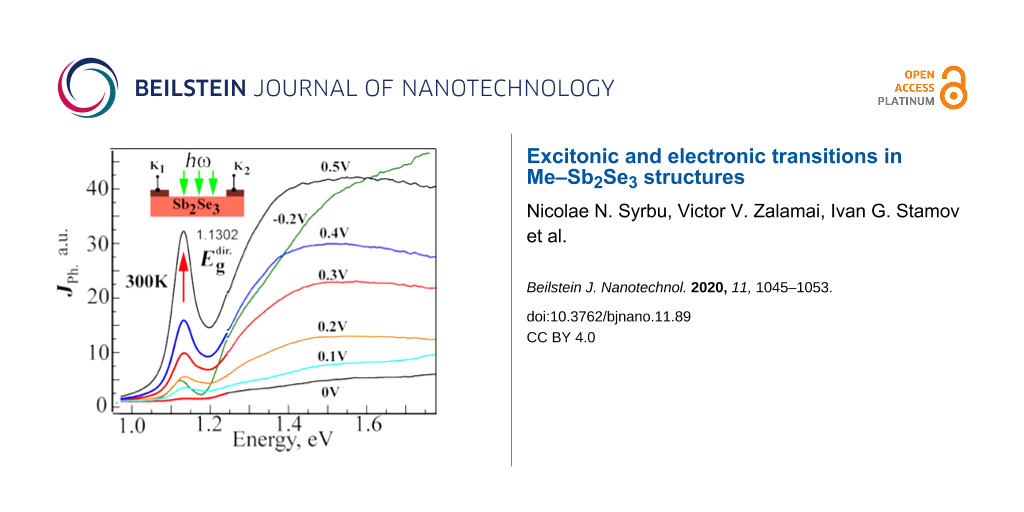
In order to investigate the electrical and photoelectric properties of the metal–antimony selenide (In–Sb2Se3) contacts, the structures were obtained by either thermal sputtering under vacuum or electrochemical deposition onto the cleaved faces of single crystals (Figure 3A). Current–voltage characteristics suggest that the contacts have an ohmic behavior. The impedance has a frequency dependence that is characteristic of the conductivity hopping mechanism which in turn is independent of the metal type and the deposition method used. The photocurrent increases when the energy of the photons increases in the Schottky barriers when the transparent contacts are illuminated. The structures with the contacts deposited onto one side of the crystal are photosensitive. At the same time, the contact deposition onto opposite sides of the crystal planes leads to the appearance of a photo-electromotive force (EMF) with a magnitude of up to 150 mV. The photocurrent increases when a positive voltage is applied to the illuminated electrode and it decreases to zero when a negative voltage is applied. The nature of the photoelectric effect cannot be associated with the contact-EMF effect since there is no band bending at the semiconductor surface region. On the other hand, the photo-EMF effect, in this case, may be associated with the Dember effect.
The photoconductivity and photo-EMF spectra in the absorption edge region show a broad band with maximum values at 1.187 eV (Е⟂с) and 1.167 eV (Е||с) (Figure 3A) which are associated with the light absorption at the direct transitions in the interband gap minimum region. It is highly likely that the photoconductivity maxima are due to excitonic ground states (n = 1) in the aforementioned polarization conditions. In addition, the photocurrent increases when the bias increases. For the unpolarized light case, the photoconductivity spectra have a narrow maximum at 1.15 eV when different voltages are applied to the K1 and K2 contacts belonging to the structure shown in the Figure 3B insert. The maximum intensity increases when the voltage between the contacts increase which can be associated with the electronic transitions in the absorption spectra at 1.17 eV and 1.19 eV. When the applied voltage increases the photocurrent signal also increases in the region of higher energies (1.2–1.8 eV), reaching a maximum at 1.5–1.6 eV. The maximum photocurrent value at 1.15 eV is due to excitonic states at the direct electronic transitions between V1–C1 bands. The increase in intensity with the applied voltage confirms the excitonic character of the maximum, which is consistent with the fact that the binding energy of these excitons is 130–136 meV.
The In–Sb2Se3 structures, in which the contacts were deposited by electrochemical methods, show photosensitivity over a wide energy range (1–1.8 eV, Figure 4). When a voltage range from 0 to 2 V was applied to the indium contacts, the photoconductivity maximum was registered at 1.168 eV for both polarization cases (E⟂c and E||c). This happens due to the direct electronic transitions in the bandgap minimum. The maxima D at 1.46 eV and F at 1.67 eV are observed in the photoconductivity spectra at the energy range between 1.3–1.8 eV for the E⟂c polarization case (Figure 4). For the E||c polarization condition, a lower maximum S is observed at 1.60 eV. All these maxima can be attributed to the direct electronic transitions in the Brillouin zone.
![[2190-4286-11-89-4]](/bjnano/content/figures/2190-4286-11-89-4.png?scale=2.0&max-width=1024&background=FFFFFF)
Figure 4: The photoconductivity spectra registered when 2 V is applied to the In–Sb2Se3 contacts (Figure 3A, insert) under the E||c and E⟂c polarization conditions.
Figure 4: The photoconductivity spectra registered when 2 V is applied to the In–Sb2Se3 contacts (Figure 3A, insert) u...
The maxima observed for the reflection spectra (room temperature, E||c) are at 1.164 eV and 1.325 eV due to the ground states nA = 1 and nC = 1 for the A and C excitonic series, respectively. For the Е⟂с case, the reflection spectra maxima are at 1.191 eV and 1.467 eV due to the ground states for B and D excitons, respectively. A weaker shoulder S at 1.6 eV and a maximum G at 1.807 eV are measured for the E||c polarization case at higher energies. For E⟂c the polarization maximum F is at 1.671 eV (Figure 5A). There is good agreement between the maxima in the reflection (Figure 5) and in the photoconductivity spectra (Figure 4); therefore, these values can be attributed to the direct excitonic state transitions in the Brillouin zone.
![[2190-4286-11-89-5]](/bjnano/content/figures/2190-4286-11-89-5.png?scale=2.0&max-width=1024&background=FFFFFF)
Figure 5: (A) The reflection spectra of the Sb2Se3 crystal measured at room temperature for both E||c and E⟂c polarization conditions. (B) The edge absorption of the Sb2Sе3 crystal with a thickness d = 1.3 μm for Е||с and Е⟂с polarization conditions at a temperature of 10 K.
Figure 5: (A) The reflection spectra of the Sb2Se3 crystal measured at room temperature for both E||c and E⟂c...
The excitonic nature of the maxima detected in the reflection spectra is also confirmed by the absorption spectra measurements performed at low temperatures (Figure 5B). For the Е||c case, when the temperature decreases to 10 K, a maximum is detected at 1.299 eV which is caused by the exciton ground states nA = 1, conventionally designated as the A series. For the same polarization case, another maximum nС = 1 is detected at 1.347 eV, which is caused by the ground state of the C excitonic series. For the E⟂c polarization case six maxima are detected. In the long-wavelength region, a maximum is detected at 1.312 eV, which is caused by the B series. At 1.410 eV and 1.429 eV, the excited states nB = 2 and nB = 3 of the B excitonic series are observed. In the high-energy region, the maximum nD = 1 is detected at 1.538 eV and a weaker peak is detected at 1.588 eV, which is formed by the D excitonic series in the vicinity of another pair of bands. To determine the main parameters of the excitonic series, the profiles of the measured reflection spectra of the A and B excitons (experimental data) are calculated based on the dispersion ratios in the single-oscillator and multi-oscillator models, according to a method described in our previous work [26].
Figure 6 shows the experimentally measured and the calculated profiles of the reflection spectra for both Е||с and Е⟂с polarization cases at 300 K. The calculations showed that for the polarization Е||с the background dielectric constant (εb) is equal to 7.5, the energy of the transversal exciton (ωТ) is 1.192 eV, the longitudinal-transversal splitting (ωLT) is 15 meV, the damping factor (γ) is 110 and the translational mass of the exciton (M) is 3.5m0 (Table 2). For the excitonic series С the following parameters were calculated: ωТ = 1.310 eV, ωLT = 17 meV, γ = 150 and M = 3.9m0. For the E⟂c polarization case the calculations of the reflection spectra profiles gave the following parameters: εb = 7.5, ωТ = 1.219 eV, ωLT = 14 meV, γ = 161, and M = 4.5m0.
![[2190-4286-11-89-6]](/bjnano/content/figures/2190-4286-11-89-6.png?scale=2.0&max-width=1024&background=FFFFFF)
Figure 6: The experimentally measured (exp.) and calculated (calc.) profiles of the reflection spectra for the Е||с (A) and Е⟂с (B) polarization cases at 300 K.
Figure 6: The experimentally measured (exp.) and calculated (calc.) profiles of the reflection spectra for th...
Table 2: Exciton parameters of the Sb2Se3 crystals (data outside brackets: from the reflection spectra, data inside brackets: from the absorption spectra).
| Exciton state | E||c, A-exc. | E⟂c, B-exc. | E⟂c, C-exc. | E⟂c, D-exc. |
|
R, 300 K/
(α, 11 K) |
R, 300 K/
(α, 11 K) |
R, 300 K/
(α,11 K) |
R, 300 K/
(α, 11 K) |
|
| n = 1, eV |
1.164/
(1.299) |
1.191/
(1.312) |
1.310/
(1.347) |
1.522/
(1.538) |
| n = 2, eV | – |
1.317/
(1.410) |
1.372 |
/
(1.588) |
| n = 3, eV | – | (1.429) | – | – |
| ωLT, meV | 15.0 | 14.0 | 17.0 | – |
| Ry, eV | – |
0.168/
(0.130) |
0.082 | 0.067 |
| Eg, eV | – |
1.359/
(1.442) |
1.392 | 1.589 |
| εb | 7.5 | 7.5 | – | 8.5 |
| μ*, m0 | 0.56 | 0.56 | – | 0.49 |
| M, m0 | 3.5 | 4.5 | 3.9 | 3.9 |
| mc*, m0 | 0.67 | 0.67 | 0.67 | 0.67 |
| mv1*, m0 | 3.32 | – | – | – |
| mv2*, m0 | – | 3.83 | – | – |
| mv3*, m0 | – | – | 3.23 | – |
| mv4*, m0 | – | – | – | 3.32 |
By using the obtained experimental data and the known relation ![[Graphic 1]](/bjnano/content/inline/2190-4286-11-89-i1.svg?max-width=637&scale=1.18182) where RH is the Rydberg energy of a hydrogen atom (13.6 eV) and Ry is the binding energy for the corresponding exciton (Rydberg constant), the reduced effective mass (μ*) is calculated for the excitons A, B, C and D. For excitons A and B when the background dielectric constant is εb = 7.5 and the binding energy is Ry = 130–136 meV the reduced exciton mass is μ* = 0.56m0. For the exciton series C at εb = 7.5 and at the binding energy Ry = 82 meV, the reduced mass of the exciton is μ* = 0.49m0. The Bohr radius (αB) for the S state of the A exciton is 0.3 × 10⁻⁵ cm and for the B exciton it is αB = 0.2 × 10⁻⁵ cm. Considering that the exciton mass M is equal to the sum of the masses of holes and electrons, mv* + mc*, and the reduced mass 1/µ* is equal to (1/mv*) + (1/mc*), from the experimentally estimated mass values of M and µ*, the effective mass is estimated for the electrons in the conduction band mc* = 0.67m0 and for the holes in the valence bands mv1* = 3.32m0, mv2* = 3.83m0, mv3* = 3.23m0 and mv4* = 3.32m0 (Table 2). The excitonic parameters calculated here correlate with the previously published data [18], where it was stated that Frenkel excitons exist in the Sb2S3 crystals with a binding energy Ry = 0.1 eV and effective mass mc* = 1.035m0, mv1* = 1.843m0. A similar approach that was used in our previous work to study the Sn2S3 crystals was also used here for the calculation of the effective mass of electrons and holes in the bands located at the Brillouin zone center. The magnitudes of the effective mass of the electrons (mc* = 1.08m0) at the bottom of the conduction band and of the holes at the top of four valence bands (mv1*, mv2* = 2.91m0 and mv3*, mv4* = 3.12m0) were estimated [24]. The bandgap was calculated based on the positions of the ground and excited states of the observed excitons. The well-known formula Eg = Ei + Ry/n2 was used for this calculation, where Eg is the bandgap energy, Ei corresponds to the positions of the ground (n = 1) and excited (n = 2, 3, 4…) states of the exciton, Ry is the exciton binding energy (Rydberg constant) and n = 1, 2, 3 … are the main quantum numbers. First, from the positions of the ground and excited states, the Rydberg constant was calculated. Then the bandgap energy is estimated.
where RH is the Rydberg energy of a hydrogen atom (13.6 eV) and Ry is the binding energy for the corresponding exciton (Rydberg constant), the reduced effective mass (μ*) is calculated for the excitons A, B, C and D. For excitons A and B when the background dielectric constant is εb = 7.5 and the binding energy is Ry = 130–136 meV the reduced exciton mass is μ* = 0.56m0. For the exciton series C at εb = 7.5 and at the binding energy Ry = 82 meV, the reduced mass of the exciton is μ* = 0.49m0. The Bohr radius (αB) for the S state of the A exciton is 0.3 × 10⁻⁵ cm and for the B exciton it is αB = 0.2 × 10⁻⁵ cm. Considering that the exciton mass M is equal to the sum of the masses of holes and electrons, mv* + mc*, and the reduced mass 1/µ* is equal to (1/mv*) + (1/mc*), from the experimentally estimated mass values of M and µ*, the effective mass is estimated for the electrons in the conduction band mc* = 0.67m0 and for the holes in the valence bands mv1* = 3.32m0, mv2* = 3.83m0, mv3* = 3.23m0 and mv4* = 3.32m0 (Table 2). The excitonic parameters calculated here correlate with the previously published data [18], where it was stated that Frenkel excitons exist in the Sb2S3 crystals with a binding energy Ry = 0.1 eV and effective mass mc* = 1.035m0, mv1* = 1.843m0. A similar approach that was used in our previous work to study the Sn2S3 crystals was also used here for the calculation of the effective mass of electrons and holes in the bands located at the Brillouin zone center. The magnitudes of the effective mass of the electrons (mc* = 1.08m0) at the bottom of the conduction band and of the holes at the top of four valence bands (mv1*, mv2* = 2.91m0 and mv3*, mv4* = 3.12m0) were estimated [24]. The bandgap was calculated based on the positions of the ground and excited states of the observed excitons. The well-known formula Eg = Ei + Ry/n2 was used for this calculation, where Eg is the bandgap energy, Ei corresponds to the positions of the ground (n = 1) and excited (n = 2, 3, 4…) states of the exciton, Ry is the exciton binding energy (Rydberg constant) and n = 1, 2, 3 … are the main quantum numbers. First, from the positions of the ground and excited states, the Rydberg constant was calculated. Then the bandgap energy is estimated.
In the Sb2Se3 and Sb2S3 crystals, the theoretical calculation of the band structure over a wide energy range was performed in several studies [6,8,10,19]; however, the obtained results were contradictory and the inconsistencies were related to the assignment of the actual points in the Brillouin zone. For all the previous studies [6,8,10,19] the valence bands had the maximum in the Brillouin zone center (in k = 0, Г-point) whereas the minimum in the conduction band was found to be in different points of the Brillouin zone. For example, a few studies [8,10,19] showed that the minimum was localized in the Z point whereas others [6] found the minimum in the X point. In addition, for the Sb2S3 crystals [20], the minimum energy interval corresponded to direct transitions in the center of the Brillouin zone (Г-point). For the Sb2Se3 crystals the top of the valence band was positioned between the Γ and S points, while the bottom of the conduction band was in the Γ point. Given the inconsistency in the literature, our results were discussed based on theoretical calculations performed by Koç and collaborators [20]. A similar approach was used to interpret our previous data for the Sb2S3 crystals [24]. Based on the results by Koç et al. [20], Figure 7 illustrates the band structure fragment in the interband minimum region. As mentioned previously, Koç and collaborators [20] calculated and built a wavevector space for both crystals (Sb2S3 and Sb2Se3) band structures. Based on these data an interpretation was made in terms of the electron transitions in the framework of the calculated band structure. As mentioned, a few previous studies have shown that the absorption edge was formed by indirect transitions in Sb2Se3. However, the data presented here does not confirm entirely the previous findings and it does not refute the existence of indirect transitions given that more studies (like the ones made for Ge, Si, GaP, etc.) need to be performed in order to clarify those issues, ideally with purely grown crystals. We do not negate the existence of indirect transitions as we do not have such experimental data. Therefore, a focus will be given on the direct transitions that were experimentally observed (Figure 7).
![[2190-4286-11-89-7]](/bjnano/content/figures/2190-4286-11-89-7.png?scale=2.0&max-width=1024&background=FFFFFF)
Figure 7: (A) The energy band structure of the Sb2Sе3 crystals. Insert illustrates the Brillouin zone. (B) Transformation from the tetrahedral to orthorhombic symmetry due to the spin–orbit interaction and the crystal field in the center of the Brillouin zone. Figure 7B adapted with permission from [24], copyright 2020 Elsevier.
Figure 7: (A) The energy band structure of the Sb2Sе3 crystals. Insert illustrates the Brillouin zone. (B) Tr...
The excitonic series A, B, C, and D is formed by the electrons in the conduction band C1 (with Г6 symmetry) and the holes in the valence bands V1, V2, V3, and V4 (with Г7, Г6, Г7, and Г6 symmetries), respectively [27]. Considering that the bands originate from the structures with a higher symmetry (tetragonal) to the structures with an orthorhombic symmetry (D2h), it should be noted that the bands in k = 0 are split by a crystal field and a spin–orbit interaction [27]. The lower conduction band is formed from the Г1 states and acquires the Г6 (Г7) symmetry, while the upper valence bands of V1, V2, V3, and V4 have the Г7, Г6, Г7, and Г6 symmetry, respectively. The interaction between the electrons from the Г6 conduction band and the holes from the Г7 valence band is determined by the product of the irreducible representation Г1 × Г6 × Г7 = Г3 + Г4 + Г5. As a result of this interaction, in the long-wavelength region, an exciton Г4 is allowed in polarization E||c, Г5 is allowed in polarization E⟂c and Г3 is forbidden in both polarization conditions. The interaction between the electrons from the C1 conduction band (Г6 symmetry) with the holes from the V2 valence band (Г6 symmetry) causes the appearance of three excitonic series: Г1, Г2 and Г5. According to the selection rules for the Е⟂с polarization case, the Г5 excitons are allowed whereas the Г1 and Г2 excitons are both forbidden. A similar approach was used when the Sb2S3 single crystals were investigated [24]. Since the Sn2S3 and Sn2Se3 crystals have the same crystal structure and a similar band structure (only with a different bandgap) the excitons observed had the same symmetries. Based on the obtained experimental data, the splitting between the upper valence bands, V1 and V2, in the center of the Brillouin zone is 13 meV, whereas the splitting between V2 and V3 is 35 meV and between V3 and V4 is 191 meV.
Besides the excitonic peaks (A, B, C and D), the features a1 (2.090 eV), a2 (3.059 eV), a3 (3.365 eV), a4 (3.822 eV), a5 (4.432 eV), a6 (5.009 eV), a7 (5.281 eV), a8 (5.466 eV) and a9 (5.815 eV) are also observed in the reflection spectra (Figure 8). These spectra were measured at room temperature over a wide energy range (1–6 eV) under the E||c and E⟂c polarization conditions. The observed reflection peaks can be associated with the direct electronic transitions at actual points of the Brillouin zone. In the Е⟂c polarization, the reflection spectra maxima b1 (2.167 eV), b2 (2.439 eV), b3 (2.875 eV), b4 (3.191 eV), b5 (3.485 eV), b6 (4.040 eV), b7 (4.509 eV), b8 (5.391 eV), b9 (5.685 eV) and b10 (6.045 eV) can be identified. The maxima a1, b1, b2, and b3 are most likely due to the electronic transitions from the valence bands V1, V2, V3 and V4 to the conduction band C2 in the Brillouin zone center. The maxima localized in the high-energy region of the reflection spectra a2, a3, a4, a5, b4, b5, b6 and b7 are most likely associated with the transitions from the upper valence bands V1, V2, V3 and V4 to the conduction bands C3 and C4 also in k = 0. The maxima of the reflection spectra in the high-energy range (4–6 eV) are possibly from the valence band maxima in the Y and S points of the Brillouin zone.
![[2190-4286-11-89-8]](/bjnano/content/figures/2190-4286-11-89-8.png?scale=2.0&max-width=1024&background=FFFFFF)
Figure 8: The reflection spectra of the Sb2Se3 crystals measured at room temperature under Е||с and Е⟂с polarization conditions.
Figure 8: The reflection spectra of the Sb2Se3 crystals measured at room temperature under Е||с and Е⟂с polar...
Conclusion
The ground and excited states of four excitonic series (A, B, C, and D) formed in the bandgap minimum region were identified based on the studies of the optical properties of the Sb2Se3 single crystals performed at different temperatures. Taking into account the energy position of the excitonic ground and excited states, the binding energy of the excitons and the valence bands V1–V4 were determined. In the Brillouin zone Г-point, the calculated electron effective mass mc* was 0.67m0, and the values of the hole effective masses mv1*, mv2*, mv3* and mv4* were 3.32m0, 3.83m0, 3.23m0 and 3.32m0, respectively. The V1–V2 valence band splitting in the center of the Brillouin zone by a crystal field (Δcr = 13 meV) and the spin–orbit interaction (Δso = 35 meV) were determined. The bands V3–V4 were split by 191 meV. The observed features were discussed based on the theoretical calculation of the energy band structures and the excitonic band symmetries in the Brillouin zone center for crystals with an orthorhombic symmetry (Pnma). The In–Sb2Se3 structures were generated either by thermal sputtering under vacuum or by electrochemical deposition. The photoconductivity spectra at different applied voltages were investigated. The features associated with the excitonic states were shown in the measured photoconductivity spectra.
References
-
Zhou, Y.; Wang, L.; Chen, S.; Qin, S.; Liu, X.; Chen, J.; Xue, D.-J.; Luo, M.; Cao, Y.; Cheng, Y.; Sargent, E. H.; Tang, J. Nat. Photonics 2015, 9, 409–415. doi:10.1038/nphoton.2015.78
Return to citation in text: [1] -
Zeng, K.; Xue, D.-J.; Tang, J. Semicond. Sci. Technol. 2016, 31, 063001. doi:10.1088/0268-1242/31/6/063001
Return to citation in text: [1] -
Wang, L.; Li, D.-B.; Li, K.; Chen, C.; Deng, H.-X.; Gao, L.; Zhao, Y.; Jiang, F.; Li, L.; Huang, F.; He, Y.; Song, H.; Niu, G.; Tang, J. Nat. Energy 2017, 2, 17046. doi:10.1038/nenergy.2017.46
Return to citation in text: [1] [2] [3] -
Chen, C.; Wang, L.; Gao, L.; Nam, D.; Li, D.; Li, K.; Zhao, Y.; Ge, C.; Cheong, H.; Liu, H.; Song, H.; Tang, J. ACS Energy Lett. 2017, 2, 2125–2132. doi:10.1021/acsenergylett.7b00648
Return to citation in text: [1] [2] -
Messina, S.; Nair, M. T. S.; Nair, P. K. J. Electrochem. Soc. 2009, 156, H327. doi:10.1149/1.3089358
Return to citation in text: [1] [2] [3] -
El-Shair, H.; Ibrahim, A.; Abd El-Wahabb, E.; Afify, M.; Abd El-Salam, F. Vacuum 1991, 42, 911–914. doi:10.1016/0042-207x(91)90557-y
Return to citation in text: [1] [2] [3] [4] [5] [6] [7] -
Zhou, Y.; Leng, M.; Xia, Z.; Zhong, J.; Song, H.; Liu, X.; Yang, B.; Zhang, J.; Chen, J.; Zhou, K.; Han, J.; Cheng, Y.; Tang, J. Adv. Energy Mater. 2014, 4, 1301846. doi:10.1002/aenm.201301846
Return to citation in text: [1] [2] [3] -
Chen, C.; Li, W.; Zhou, Y.; Chen, C.; Luo, M.; Liu, X.; Zeng, K.; Yang, B.; Zhang, C.; Han, J.; Tang, J. Appl. Phys. Lett. 2015, 107, 043905. doi:10.1063/1.4927741
Return to citation in text: [1] [2] [3] [4] [5] [6] [7] -
Voutsas, G. P.; Papazoglou, A. G.; Rentzeperis, P. J.; Siapkas, D. Z. Kristallogr. 1985, 171, 261–268. doi:10.1524/zkri.1985.171.3-4.261
Return to citation in text: [1] -
Mueller, R.; Wood, C. J. Non-Cryst. Solids 1972, 7, 301–308. doi:10.1016/0022-3093(72)90266-9
Return to citation in text: [1] [2] [3] [4] [5] [6] -
Ko, T.-Y.; Shellaiah, M.; Sun, K. W. Sci. Rep. 2016, 6, 35086. doi:10.1038/srep35086
Return to citation in text: [1] [2] -
Fourspring, P. M.; DePoy, D. M.; Rahmlow, T. D., Jr.; Lazo-Wasem, J. E.; Gratrix, E. J. Appl. Opt. 2006, 45, 1356–1358. doi:10.1364/ao.45.001356
Return to citation in text: [1] -
Arun, P.; Vedeshwar, A. G.; Mehra, N. C. J. Phys. D: Appl. Phys. 1999, 32, 183–190. doi:10.1088/0022-3727/32/3/001
Return to citation in text: [1] -
Song, H.; Li, T.; Zhang, J.; Zhou, Y.; Luo, J.; Chen, C.; Yang, B.; Ge, C.; Wu, Y.; Tang, J. Adv. Mater. (Weinheim, Ger.) 2017, 29, 1700441. doi:10.1002/adma.201700441
Return to citation in text: [1] -
Kurumada, M.; Suzuki, H.; Kimura, Y.; Saito, Y.; Kaito, C. J. Cryst. Growth 2003, 250, 444–449. doi:10.1016/s0022-0248(02)02463-6
Return to citation in text: [1] [2] -
Gilbert, L. R.; Van Pelt, B.; Wood, C. J. Phys. Chem. Solids 1974, 35, 1629–1632. doi:10.1016/s0022-3697(74)80175-7
Return to citation in text: [1] -
Kutasov, V. A. Shifting the maximum figure-of-merit of (Bi, Sb)2(Te, Se)3 thermoelectrics to lower temperatures. Thermoelectrics Handbook; CRC Press: Boca Raton, FL, USA, 2005; pp 18–37.
Return to citation in text: [1] -
Liu, X.; Chen, J.; Luo, M.; Leng, M.; Xia, Z.; Zhou, Y.; Qin, S.; Xue, D.-J.; Lv, L.; Huang, H.; Niu, D.; Tang, J. ACS Appl. Mater. Interfaces 2014, 6, 10687–10695. doi:10.1021/am502427s
Return to citation in text: [1] [2] -
Zhang, Y.; Li, G.; Zhang, B.; Zhang, L. Mater. Lett. 2004, 58, 2279–2282. doi:10.1016/j.matlet.2004.02.006
Return to citation in text: [1] [2] [3] [4] [5] -
Koç, H.; Mamedov, A. M.; Deligoz, E.; Ozisik, H. Solid State Sci. 2012, 14, 1211–1220. doi:10.1016/j.solidstatesciences.2012.06.003
Return to citation in text: [1] [2] [3] [4] [5] [6] -
Černošková, E.; Todorov, R.; Černošek, Z.; Holubová, J.; Beneš, L. J. Therm. Anal. Calorim. 2014, 118, 105–110. doi:10.1007/s10973-014-4000-3
Return to citation in text: [1] [2] -
El-Sayad, E. A. J. Non-Cryst. Solids 2008, 354, 3806–3811. doi:10.1016/j.jnoncrysol.2008.05.004
Return to citation in text: [1] -
Vadapoo, R.; Krishnan, S.; Yilmaz, H.; Marin, C. Phys. Status Solidi B 2011, 248, 700–705. doi:10.1002/pssb.201046225
Return to citation in text: [1] -
Beril, S. I.; Stamov, I. G.; Tiron, A. V.; Zalamai, V. V.; Syrbu, N. N. Opt. Mater. 2020, 101, 109737. doi:10.1016/j.optmat.2020.109737
Return to citation in text: [1] [2] [3] [4] [5] [6] [7] -
Green, M. A.; Emery, K.; Hishikawa, Y.; Warta, W.; Dunlop, E. D.; Levi, D. H.; Ho-Baillie, A. W. Y. Prog. Photovoltaics 2017, 25, 3–13. doi:10.1002/pip.2855
Return to citation in text: [1] -
Syrbu, N. N.; Ursaki, V. V. Exciton polariton dispersion in multinary compounds. In Exciton Quasiparticles: Theory, Dynamicsand Applications; Bergin, R. M., Ed.; Nova Science Publishers Inc., 2010; pp 1–130.
Return to citation in text: [1] -
Kovalev, O. V. Irreducible and Induced Representations and Corepresentations of Fedorov Groups; Nauka: Moscow, Russia, 1986.
(in Russian).
Return to citation in text: [1] [2]
| 6. | El-Shair, H.; Ibrahim, A.; Abd El-Wahabb, E.; Afify, M.; Abd El-Salam, F. Vacuum 1991, 42, 911–914. doi:10.1016/0042-207x(91)90557-y |
| 20. | Koç, H.; Mamedov, A. M.; Deligoz, E.; Ozisik, H. Solid State Sci. 2012, 14, 1211–1220. doi:10.1016/j.solidstatesciences.2012.06.003 |
| 20. | Koç, H.; Mamedov, A. M.; Deligoz, E.; Ozisik, H. Solid State Sci. 2012, 14, 1211–1220. doi:10.1016/j.solidstatesciences.2012.06.003 |
| 1. | Zhou, Y.; Wang, L.; Chen, S.; Qin, S.; Liu, X.; Chen, J.; Xue, D.-J.; Luo, M.; Cao, Y.; Cheng, Y.; Sargent, E. H.; Tang, J. Nat. Photonics 2015, 9, 409–415. doi:10.1038/nphoton.2015.78 |
| 2. | Zeng, K.; Xue, D.-J.; Tang, J. Semicond. Sci. Technol. 2016, 31, 063001. doi:10.1088/0268-1242/31/6/063001 |
| 3. | Wang, L.; Li, D.-B.; Li, K.; Chen, C.; Deng, H.-X.; Gao, L.; Zhao, Y.; Jiang, F.; Li, L.; Huang, F.; He, Y.; Song, H.; Niu, G.; Tang, J. Nat. Energy 2017, 2, 17046. doi:10.1038/nenergy.2017.46 |
| 4. | Chen, C.; Wang, L.; Gao, L.; Nam, D.; Li, D.; Li, K.; Zhao, Y.; Ge, C.; Cheong, H.; Liu, H.; Song, H.; Tang, J. ACS Energy Lett. 2017, 2, 2125–2132. doi:10.1021/acsenergylett.7b00648 |
| 5. | Messina, S.; Nair, M. T. S.; Nair, P. K. J. Electrochem. Soc. 2009, 156, H327. doi:10.1149/1.3089358 |
| 6. | El-Shair, H.; Ibrahim, A.; Abd El-Wahabb, E.; Afify, M.; Abd El-Salam, F. Vacuum 1991, 42, 911–914. doi:10.1016/0042-207x(91)90557-y |
| 7. | Zhou, Y.; Leng, M.; Xia, Z.; Zhong, J.; Song, H.; Liu, X.; Yang, B.; Zhang, J.; Chen, J.; Zhou, K.; Han, J.; Cheng, Y.; Tang, J. Adv. Energy Mater. 2014, 4, 1301846. doi:10.1002/aenm.201301846 |
| 8. | Chen, C.; Li, W.; Zhou, Y.; Chen, C.; Luo, M.; Liu, X.; Zeng, K.; Yang, B.; Zhang, C.; Han, J.; Tang, J. Appl. Phys. Lett. 2015, 107, 043905. doi:10.1063/1.4927741 |
| 9. | Voutsas, G. P.; Papazoglou, A. G.; Rentzeperis, P. J.; Siapkas, D. Z. Kristallogr. 1985, 171, 261–268. doi:10.1524/zkri.1985.171.3-4.261 |
| 10. | Mueller, R.; Wood, C. J. Non-Cryst. Solids 1972, 7, 301–308. doi:10.1016/0022-3093(72)90266-9 |
| 21. | Černošková, E.; Todorov, R.; Černošek, Z.; Holubová, J.; Beneš, L. J. Therm. Anal. Calorim. 2014, 118, 105–110. doi:10.1007/s10973-014-4000-3 |
| 22. | El-Sayad, E. A. J. Non-Cryst. Solids 2008, 354, 3806–3811. doi:10.1016/j.jnoncrysol.2008.05.004 |
| 23. | Vadapoo, R.; Krishnan, S.; Yilmaz, H.; Marin, C. Phys. Status Solidi B 2011, 248, 700–705. doi:10.1002/pssb.201046225 |
| 24. | Beril, S. I.; Stamov, I. G.; Tiron, A. V.; Zalamai, V. V.; Syrbu, N. N. Opt. Mater. 2020, 101, 109737. doi:10.1016/j.optmat.2020.109737 |
| 3. | Wang, L.; Li, D.-B.; Li, K.; Chen, C.; Deng, H.-X.; Gao, L.; Zhao, Y.; Jiang, F.; Li, L.; Huang, F.; He, Y.; Song, H.; Niu, G.; Tang, J. Nat. Energy 2017, 2, 17046. doi:10.1038/nenergy.2017.46 |
| 7. | Zhou, Y.; Leng, M.; Xia, Z.; Zhong, J.; Song, H.; Liu, X.; Yang, B.; Zhang, J.; Chen, J.; Zhou, K.; Han, J.; Cheng, Y.; Tang, J. Adv. Energy Mater. 2014, 4, 1301846. doi:10.1002/aenm.201301846 |
| 8. | Chen, C.; Li, W.; Zhou, Y.; Chen, C.; Luo, M.; Liu, X.; Zeng, K.; Yang, B.; Zhang, C.; Han, J.; Tang, J. Appl. Phys. Lett. 2015, 107, 043905. doi:10.1063/1.4927741 |
| 6. | El-Shair, H.; Ibrahim, A.; Abd El-Wahabb, E.; Afify, M.; Abd El-Salam, F. Vacuum 1991, 42, 911–914. doi:10.1016/0042-207x(91)90557-y |
| 8. | Chen, C.; Li, W.; Zhou, Y.; Chen, C.; Luo, M.; Liu, X.; Zeng, K.; Yang, B.; Zhang, C.; Han, J.; Tang, J. Appl. Phys. Lett. 2015, 107, 043905. doi:10.1063/1.4927741 |
| 10. | Mueller, R.; Wood, C. J. Non-Cryst. Solids 1972, 7, 301–308. doi:10.1016/0022-3093(72)90266-9 |
| 19. | Zhang, Y.; Li, G.; Zhang, B.; Zhang, L. Mater. Lett. 2004, 58, 2279–2282. doi:10.1016/j.matlet.2004.02.006 |
| 20. | Koç, H.; Mamedov, A. M.; Deligoz, E.; Ozisik, H. Solid State Sci. 2012, 14, 1211–1220. doi:10.1016/j.solidstatesciences.2012.06.003 |
| 5. | Messina, S.; Nair, M. T. S.; Nair, P. K. J. Electrochem. Soc. 2009, 156, H327. doi:10.1149/1.3089358 |
| 6. | El-Shair, H.; Ibrahim, A.; Abd El-Wahabb, E.; Afify, M.; Abd El-Salam, F. Vacuum 1991, 42, 911–914. doi:10.1016/0042-207x(91)90557-y |
| 7. | Zhou, Y.; Leng, M.; Xia, Z.; Zhong, J.; Song, H.; Liu, X.; Yang, B.; Zhang, J.; Chen, J.; Zhou, K.; Han, J.; Cheng, Y.; Tang, J. Adv. Energy Mater. 2014, 4, 1301846. doi:10.1002/aenm.201301846 |
| 20. | Koç, H.; Mamedov, A. M.; Deligoz, E.; Ozisik, H. Solid State Sci. 2012, 14, 1211–1220. doi:10.1016/j.solidstatesciences.2012.06.003 |
| 27. |
Kovalev, O. V. Irreducible and Induced Representations and Corepresentations of Fedorov Groups; Nauka: Moscow, Russia, 1986.
(in Russian). |
| 3. | Wang, L.; Li, D.-B.; Li, K.; Chen, C.; Deng, H.-X.; Gao, L.; Zhao, Y.; Jiang, F.; Li, L.; Huang, F.; He, Y.; Song, H.; Niu, G.; Tang, J. Nat. Energy 2017, 2, 17046. doi:10.1038/nenergy.2017.46 |
| 4. | Chen, C.; Wang, L.; Gao, L.; Nam, D.; Li, D.; Li, K.; Zhao, Y.; Ge, C.; Cheong, H.; Liu, H.; Song, H.; Tang, J. ACS Energy Lett. 2017, 2, 2125–2132. doi:10.1021/acsenergylett.7b00648 |
| 5. | Messina, S.; Nair, M. T. S.; Nair, P. K. J. Electrochem. Soc. 2009, 156, H327. doi:10.1149/1.3089358 |
| 6. | El-Shair, H.; Ibrahim, A.; Abd El-Wahabb, E.; Afify, M.; Abd El-Salam, F. Vacuum 1991, 42, 911–914. doi:10.1016/0042-207x(91)90557-y |
| 8. | Chen, C.; Li, W.; Zhou, Y.; Chen, C.; Luo, M.; Liu, X.; Zeng, K.; Yang, B.; Zhang, C.; Han, J.; Tang, J. Appl. Phys. Lett. 2015, 107, 043905. doi:10.1063/1.4927741 |
| 10. | Mueller, R.; Wood, C. J. Non-Cryst. Solids 1972, 7, 301–308. doi:10.1016/0022-3093(72)90266-9 |
| 27. |
Kovalev, O. V. Irreducible and Induced Representations and Corepresentations of Fedorov Groups; Nauka: Moscow, Russia, 1986.
(in Russian). |
| 14. | Song, H.; Li, T.; Zhang, J.; Zhou, Y.; Luo, J.; Chen, C.; Yang, B.; Ge, C.; Wu, Y.; Tang, J. Adv. Mater. (Weinheim, Ger.) 2017, 29, 1700441. doi:10.1002/adma.201700441 |
| 15. | Kurumada, M.; Suzuki, H.; Kimura, Y.; Saito, Y.; Kaito, C. J. Cryst. Growth 2003, 250, 444–449. doi:10.1016/s0022-0248(02)02463-6 |
| 17. | Kutasov, V. A. Shifting the maximum figure-of-merit of (Bi, Sb)2(Te, Se)3 thermoelectrics to lower temperatures. Thermoelectrics Handbook; CRC Press: Boca Raton, FL, USA, 2005; pp 18–37. |
| 18. | Liu, X.; Chen, J.; Luo, M.; Leng, M.; Xia, Z.; Zhou, Y.; Qin, S.; Xue, D.-J.; Lv, L.; Huang, H.; Niu, D.; Tang, J. ACS Appl. Mater. Interfaces 2014, 6, 10687–10695. doi:10.1021/am502427s |
| 20. | Koç, H.; Mamedov, A. M.; Deligoz, E.; Ozisik, H. Solid State Sci. 2012, 14, 1211–1220. doi:10.1016/j.solidstatesciences.2012.06.003 |
| 13. | Arun, P.; Vedeshwar, A. G.; Mehra, N. C. J. Phys. D: Appl. Phys. 1999, 32, 183–190. doi:10.1088/0022-3727/32/3/001 |
| 19. | Zhang, Y.; Li, G.; Zhang, B.; Zhang, L. Mater. Lett. 2004, 58, 2279–2282. doi:10.1016/j.matlet.2004.02.006 |
| 24. | Beril, S. I.; Stamov, I. G.; Tiron, A. V.; Zalamai, V. V.; Syrbu, N. N. Opt. Mater. 2020, 101, 109737. doi:10.1016/j.optmat.2020.109737 |
| 12. | Fourspring, P. M.; DePoy, D. M.; Rahmlow, T. D., Jr.; Lazo-Wasem, J. E.; Gratrix, E. J. Appl. Opt. 2006, 45, 1356–1358. doi:10.1364/ao.45.001356 |
| 24. | Beril, S. I.; Stamov, I. G.; Tiron, A. V.; Zalamai, V. V.; Syrbu, N. N. Opt. Mater. 2020, 101, 109737. doi:10.1016/j.optmat.2020.109737 |
| 11. | Ko, T.-Y.; Shellaiah, M.; Sun, K. W. Sci. Rep. 2016, 6, 35086. doi:10.1038/srep35086 |
| 15. | Kurumada, M.; Suzuki, H.; Kimura, Y.; Saito, Y.; Kaito, C. J. Cryst. Growth 2003, 250, 444–449. doi:10.1016/s0022-0248(02)02463-6 |
| 16. | Gilbert, L. R.; Van Pelt, B.; Wood, C. J. Phys. Chem. Solids 1974, 35, 1629–1632. doi:10.1016/s0022-3697(74)80175-7 |
| 20. | Koç, H.; Mamedov, A. M.; Deligoz, E.; Ozisik, H. Solid State Sci. 2012, 14, 1211–1220. doi:10.1016/j.solidstatesciences.2012.06.003 |
| 24. | Beril, S. I.; Stamov, I. G.; Tiron, A. V.; Zalamai, V. V.; Syrbu, N. N. Opt. Mater. 2020, 101, 109737. doi:10.1016/j.optmat.2020.109737 |
| 24. | Beril, S. I.; Stamov, I. G.; Tiron, A. V.; Zalamai, V. V.; Syrbu, N. N. Opt. Mater. 2020, 101, 109737. doi:10.1016/j.optmat.2020.109737 |
| 24. | Beril, S. I.; Stamov, I. G.; Tiron, A. V.; Zalamai, V. V.; Syrbu, N. N. Opt. Mater. 2020, 101, 109737. doi:10.1016/j.optmat.2020.109737 |
| 6. | El-Shair, H.; Ibrahim, A.; Abd El-Wahabb, E.; Afify, M.; Abd El-Salam, F. Vacuum 1991, 42, 911–914. doi:10.1016/0042-207x(91)90557-y |
| 8. | Chen, C.; Li, W.; Zhou, Y.; Chen, C.; Luo, M.; Liu, X.; Zeng, K.; Yang, B.; Zhang, C.; Han, J.; Tang, J. Appl. Phys. Lett. 2015, 107, 043905. doi:10.1063/1.4927741 |
| 10. | Mueller, R.; Wood, C. J. Non-Cryst. Solids 1972, 7, 301–308. doi:10.1016/0022-3093(72)90266-9 |
| 19. | Zhang, Y.; Li, G.; Zhang, B.; Zhang, L. Mater. Lett. 2004, 58, 2279–2282. doi:10.1016/j.matlet.2004.02.006 |
| 24. | Beril, S. I.; Stamov, I. G.; Tiron, A. V.; Zalamai, V. V.; Syrbu, N. N. Opt. Mater. 2020, 101, 109737. doi:10.1016/j.optmat.2020.109737 |
| 6. | El-Shair, H.; Ibrahim, A.; Abd El-Wahabb, E.; Afify, M.; Abd El-Salam, F. Vacuum 1991, 42, 911–914. doi:10.1016/0042-207x(91)90557-y |
| 8. | Chen, C.; Li, W.; Zhou, Y.; Chen, C.; Luo, M.; Liu, X.; Zeng, K.; Yang, B.; Zhang, C.; Han, J.; Tang, J. Appl. Phys. Lett. 2015, 107, 043905. doi:10.1063/1.4927741 |
| 10. | Mueller, R.; Wood, C. J. Non-Cryst. Solids 1972, 7, 301–308. doi:10.1016/0022-3093(72)90266-9 |
| 19. | Zhang, Y.; Li, G.; Zhang, B.; Zhang, L. Mater. Lett. 2004, 58, 2279–2282. doi:10.1016/j.matlet.2004.02.006 |
| 26. | Syrbu, N. N.; Ursaki, V. V. Exciton polariton dispersion in multinary compounds. In Exciton Quasiparticles: Theory, Dynamicsand Applications; Bergin, R. M., Ed.; Nova Science Publishers Inc., 2010; pp 1–130. |
| 18. | Liu, X.; Chen, J.; Luo, M.; Leng, M.; Xia, Z.; Zhou, Y.; Qin, S.; Xue, D.-J.; Lv, L.; Huang, H.; Niu, D.; Tang, J. ACS Appl. Mater. Interfaces 2014, 6, 10687–10695. doi:10.1021/am502427s |
| 11. | Ko, T.-Y.; Shellaiah, M.; Sun, K. W. Sci. Rep. 2016, 6, 35086. doi:10.1038/srep35086 |
| 21. | Černošková, E.; Todorov, R.; Černošek, Z.; Holubová, J.; Beneš, L. J. Therm. Anal. Calorim. 2014, 118, 105–110. doi:10.1007/s10973-014-4000-3 |
| 25. | Green, M. A.; Emery, K.; Hishikawa, Y.; Warta, W.; Dunlop, E. D.; Levi, D. H.; Ho-Baillie, A. W. Y. Prog. Photovoltaics 2017, 25, 3–13. doi:10.1002/pip.2855 |
© 2020 Syrbu et al.; licensee Beilstein-Institut.
This is an Open Access article under the terms of the Creative Commons Attribution License (http://creativecommons.org/licenses/by/4.0). Please note that the reuse, redistribution and reproduction in particular requires that the authors and source are credited.
The license is subject to the Beilstein Journal of Nanotechnology terms and conditions: (https://www.beilstein-journals.org/bjnano)