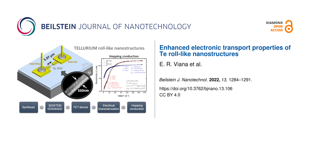
Abstract
In this work, the electronic transport properties of Te roll-like nanostructures were investigated in a broad temperature range by fabricating single-nanostructure back-gated field-effect-transistors via photolithography. These one-dimensional nanostructures, with a unique roll-like morphology, were produced by a facile synthesis and extensively studied by scanning and transmission electron microscopy. The nanostructures are made of pure and crystalline Tellurium with trigonal structure (t-Te), and exhibit p-type conductivity with enhanced field-effect hole mobility between 273 cm2/Vs at 320 K and 881 cm2/Vs at 5 K. The thermal ionization of shallow acceptors, with small ionization energy between 2 and 4 meV, leads to free-hole conduction at high temperatures. The free-hole mobility follows a negative power-law temperature behavior, with an exponent between −1.28 and −1.42, indicating strong phonon scattering in this temperature range. At lower temperatures, the electronic conduction is dominated by nearest-neighbor hopping (NNH) conduction in the acceptor band, with a small activation energy ENNH ≈ 0.6 meV and an acceptor concentration of NA ≈ 1 × 1016 cm−3. These results demonstrate the enhanced electrical properties of these nanostructures, with a small disorder, and superior quality for nanodevice applications.
Introduction
The chalcogen tellurium (Te) is a rare element (0.002 ppm) in the Earth’s crust and a well-known p-type and narrow-bandgap (≈0.35 eV at room temperature) semiconductor material. Tellurium is widely used in thermoelectric devices, piezoelectric devices, photoconductive devices, gas sensing, nonlinear optical devices, solar cells, photonic crystals, holographic recording devices, radioactive cooling devices, field-effect transistors, infrared acousto-optic deflectors, and even for antifungal activity [1-7].
Several chemical and physical methods have been recently developed to synthesize Te-based nanostructures, such as monolayers (MLs), nanoparticles (NPs), nanorods (NRs), nanowires (NWs), nanobelts (NBs), nanotubes (NTs), nanoflowers (NFs) and chiral nanostructures [6-10]. Trigonal tellurium (t-Te) MLs have also been recently proposed as a silicon successor for nanoelectronics because of their high hole mobility and current density [3]. Combining these electrical properties with the facile synthesis of one-dimensional nanostructures may bring potential applications of this material in nanoscale optoelectronic integrated devices. However, only a few works have been dedicated to studying the electrical transport in Te-based one-dimensional nanostructures [11-14]. Te NTs have shown metallic character and decreasing electrical resistivity with temperature [11]. Te NWs encapsulated in boron nitride nanotubes have shown a large current-carrying capacity and p-type semiconducting characteristics, which can be reversed to n-type behavior after capping with Al2O3 [12]. Theoretical works have also demonstrated that field-effect transistors (FETs) with single n-type trigonal Te NWs outperform the ones built with three trigonal Te NWs [14]. One important group of nanostructures, different from hollow nanotubes and solid nanowires, is NBs. NBs have a well-defined geometry with a uniform rectangular cross section along their entire length. This particular morphology makes them a strong candidate for providing a thorough understanding of dimensionally confined transport phenomena, as presented in SnO2 NBs. Moreover, strain-induced polarization charges have been studied in p-type Te NBs [13].
In this work, we have studied the electronic transport properties of a distinct one-dimensional t-Te nanostructure with a roll-like morphology, which resembles cinnamon sticks. The nanostructures were obtained by a facile PVP-assisted hydrothermal route under mild conditions. A large quantity of these polycrystalline nanostructures with a diameter between 100 and 900 nm and a wall thickness around 50 nm were synthesized and characterized by scanning electron microscopy (SEM), energy dispersive X-ray spectroscopy (EDS), transmission electron microscopy (TEM), and selected-area electron diffraction (SAED). Individual Te roll-like nanobelts were connected in back-gate FETs and measured to characterize the electronic transport as a function of temperature.
Methods
Growth of Te roll-like one-dimensional nanostructures
Te nanostructures were grown via an environmentally friendly solvothermal method by the reduction of Na2TeO3 and passivation with polyvinylpyrrolidone (PVP), as reported elsewhere [15]. The procedure described by Wu et al. [15] for the synthesis of Te NWs was followed, with the modification of increasing the autoclave heating to 200 °C. All reagents used were of analytic grade, purchased from Sigma-Aldrich Chemicals Company, and directly used without further purification.
Morphology, elemental analysis, and crystal structure
Morphology and elemental composition of the as-prepared products were characterized by scanning electron microscopy (SEM, FEI Quanta 3D FEG) at an acceleration voltage of 15.0 kV. An EDS system attached to the SEM was employed to analyze the chemical composition. TEM, high-resolution TEM (HRTEM) images, and SAED measurements were carried out in an FEI Tecnai G2-20 S-TWIN operated at 200 kV in a bright-field (BF) TEM mode. EDS point acquisitions were also performed during TEM analysis by using a silicon drift detector (SDD) from Oxford Instruments.
Electronic transport
The electronic transport properties of the sample were investigated by acquiring and modeling the transfer and gate curves of Te roll-like single-nanostructure back-gate FETs, as well as the electrical resistivity of the nanostructures as a function of temperature from 5 to 400 K. The transport measurements were carried out in a low-noise custom-made system for electrical characterization of FET devices [16-18]. FET devices were built by laser writing optical lithography on 1 × 1 cm2 degenerate Si(100) substrates covered by a 300 nm thick high-quality SiO2 layer. A Cr(10 nm)/Au(100 nm) bilayer was thermally evaporated on the sample to produce good ohmic contacts (see Supporting Information File 1). This procedure follows the methodology developed for single-nanobelt back-gated FETs [16-19], also presented in Supporting Information File 1.
Results and Discussion
The morphology of the as-prepared Te roll-like one-dimensional nanostructures is shown in Figure 1. Figure 1a and Figure 1b display a representative overview of the nanostructures, which shows that the prepared samples are composed of large-scale roll-like one-dimensional nanostructures, comparable to the shape of cinnamon sticks. Most nanostructures exhibit one flat end and a tip at the other end. The size distribution of the nanostructures is shown in the inset of Figure 1b, with a mean diameter of around 550 nm. Due to the tip at the end of the nanostructures, the diameters were measured approximately at the center part, where the size is uniform. The wall thickness of the nanostructures was found between 45 and 55 nm.
![[2190-4286-13-106-1]](/bjnano/content/figures/2190-4286-13-106-1.png?scale=2.0&max-width=1024&background=FFFFFF)
Figure 1: (a–c) SEM images at different magnifications of the roll-like Te nanostructures and (d) the EDS spectra of the sample. The inset of panel (b) shows the histogram of the diameter distribution of the nanostructures.
Figure 1: (a–c) SEM images at different magnifications of the roll-like Te nanostructures and (d) the EDS spe...
Figure 1c shows a high-magnification SEM image of the nanostructures, which vividly demonstrates the surface rugosity and the lateral opening along the growth axis of the roll-like structure. Elemental analysis of the nanostructures is shown in Figure 1d, where the strong Te peaks and a residual oxygen peak in the EDS spectrum demonstrate the chemical composition of the nanostructures. This morphology has not been reported for the hydrothermal synthesis of Te nanostructures. Though, similar morphologies have been observed in Te scroll-like nanostructures grown by reflux processes [20] or Te shuttle-like scrolled nanostructures produced by amino acid-controlled hydrothermal growth [21]. However, the typical seed at the center of the scroll-like nanostructures grown by reflux processes was not observed in our case, nor was the characteristic sharp tip at both ends of the shuttle-like scrolled Te NTs.
Figure 2 shows TEM images and the corresponding SAED patterns of the roll-like Te nanostructures. The SAED patterns shown in Figure 2b and Figure 2d were acquired from the marked circular area in Figure 2a and Figure 2c, respectively (next to the tip of the nanostructure in Figure 2b, and next to the flat end of the nanostructure in Figure 2d). Detailed analysis of the SAED patterns, acquired along the [−1−20] zone axis, using CrysTBox software [22,23] demonstrates that the roll-like nanostructure is crystalline. The one-dimensional nanostructure has the trigonal crystal structure of bulk Te, growing in the [001] orientation (indicated by a white arrow in the SAED patterns) along the longitudinal direction (parallel to the axis of the Te nanostructure) and [210] growth toward the transverse direction (perpendicular to the growth axis). The [001] growth direction is usually observed in one-dimensional t-Te nanostructures and attributed to the anisotropy of the Te crystal structure [20,21]. However, a fast Fourier transform (FFT) analysis of different areas of the HRTEM images (see Figure 3a) shows that the nanostructures are polycrystalline, with well-oriented large grains and rotated small grains at the edges. Small amorphous areas were observed at the edges of the nanostructures. However, the well-defined SAED spot patterns of Figure 2b and Figure 2d, as well as the FFT patterns in Figure 3a are a clear indication of the crystalline nature of the nanostructures. The expected diffuse halo or broad circles associated with the diffraction of amorphous/nanocrystalline materials [24] were not observed. The EDS point analysis (Figure 3b) shows that nanostructures consist of Te, in agreement with the results of the SAED analysis and the above presented EDS analysis of the sample (Figure 1d).
![[2190-4286-13-106-2]](/bjnano/content/figures/2190-4286-13-106-2.png?scale=2.0&max-width=1024&background=FFFFFF)
Figure 2: TEM image and SAED patterns of (a,b ) the flat end and (c, d) the tip of a roll-like t-Te one-dimensional nanostructure.
Figure 2: TEM image and SAED patterns of (a,b ) the flat end and (c, d) the tip of a roll-like t-Te one-dimen...
![[2190-4286-13-106-3]](/bjnano/content/figures/2190-4286-13-106-3.png?scale=2.0&max-width=1024&background=FFFFFF)
Figure 3: (a) HRTEM image of the roll-like t-Te one-dimensional nanostructure with FFT patterns from different regions of the sample. (b) EDS spectrum of the corresponding nanostructure.
Figure 3: (a) HRTEM image of the roll-like t-Te one-dimensional nanostructure with FFT patterns from differen...
The transfer characteristics of the t-Te NW-1 roll-like FET (Ids–Vg curve) at 320 and 5 K are shown in Figure 4 for Vds = 10 mV. There is a strong increase of the transconductance (gm = d(Ids)/d(Vg)) of approximately 30 times, from 0.53 nA/V at 300 K to 17 nA/V at 5 K. The p-type character of the NW is clear from these curves. Recent calculations of the band structure of t-Te have been revealed that the strong spin–orbit coupling breaks the fourfold degeneracy of the valence band at the H point of the Brillouin zone, creating two non-degenerated H4 and H5 bands and a doubly degenerated H6 band. The H4 and H5 bands contribute to the transport of free holes. However, the H6 band lies at lower energy, far from the Fermi level, and does not significantly contribute to electronic transport [25,26].
![[2190-4286-13-106-4]](/bjnano/content/figures/2190-4286-13-106-4.png?scale=2.0&max-width=1024&background=FFFFFF)
Figure 4: The transfer characteristic (Ids–Vg) of a single roll-like t-Te NW-1 one-dimensional nanostructure back-gated FET acquired at 5 and 320 K.
Figure 4: The transfer characteristic (Ids–Vg) of a single roll-like t-Te NW-1 one-dimensional nanostructure ...
Field-effect hole mobility (μh) and concentration (p) were estimated from the Ids–Vg curve using a parallel capacitor model for the FET [19,27]. This model has been successfully used to analyze the electronic properties of single semiconductor NWs of different cross sections and materials such as ZnO [27], SnO2 [16,19], and GaAs [17,18,28]. In this case, the calculations were done using μh = gmL2/(VdsCox) and p = 1/(eρμh), where gm = dIds/dVg is the transconductance, ρ is the resistivity, Cox is the gate capacitance, and e is the electron charge. For a flat nanostructure, the gate capacitance can be obtained by a simple parallel-plate approximation, given by Cox = ε0(εav)wL/dSiO2 and ρ = (R·w·t/L). Here, ε0 is the permittivity of vacuum, εav = 1.95 is the averaged relative permittivity of the SiO2/air interface of the FET [19,29]. Also, w = 550 nm, t = 50 nm, and L = 5.97 µm are the diameter of the nanostructure, the thickness of the nanostructure, and the length of the FET channel, respectively. The thickness of the dielectric layer (SiO2) in the capacitor is dSiO2 = 300 nm.
Figure 4 shows the transfer curves (Ids–Vg) of a single roll-like t-Te NW-1 one-dimensional nanostructure back-gated FET acquired at 5 and 320 K, as well as the calculated values of gm, p, and μh. The hole mobility was estimated to be μh(5 K) = 881 cm2/Vs and μh(320 K) = 273 cm2/Vs, while the hole concentration was estimated to be p(5 K) = 8.8 × 1010 cm−2 and p(320 K) = 2.8 × 1016 cm−3.
The measured electrical resistivity of NW-1 and NW-2, as a function of the temperature, from 300 down to 5 K, is shown in Figure 5. Two linear regions can be observed at high and low temperatures, corresponding to the thermally activated conduction (σTA) of free holes and the nearest-neighbor hopping (NNH, σNNH) [30-33], respectively.
![[2190-4286-13-106-5]](/bjnano/content/figures/2190-4286-13-106-5.png?scale=2.0&max-width=1024&background=FFFFFF)
Figure 5: Resistivity as a function of temperature for the t-Te roll-like NW-1 and NW-2.
Figure 5: Resistivity as a function of temperature for the t-Te roll-like NW-1 and NW-2.
In the high-temperature region, the thermally activated conduction can be expressed as [33]:
![[2190-4286-13-106-i1]](/bjnano/content/inline/2190-4286-13-106-i1.svg?max-width=590&scale=1.18182)
![[2190-4286-13-106-i2]](/bjnano/content/inline/2190-4286-13-106-i2.svg?max-width=590&scale=1.18182)
![[2190-4286-13-106-i3]](/bjnano/content/inline/2190-4286-13-106-i3.svg?max-width=590&scale=1.18182)
where µ0 is a constant. Since the mobility is mainly limited by phonon scattering at high temperatures, α is close to 3/2 [33,34]. Nveff is the effective density of states of the valence band, EA is the shallow acceptor ionization energy [33], and kB is Boltzmann’s constant.
At lower temperatures, most of the free holes are recaptured by acceptors and cannot be thermally excited back to the valence band [30,33]. In this case, the thermally activated conduction of free holes becomes less important, and hole hopping directly between acceptor states in the impurity band becomes the primary conduction mechanism [30-33]. In this case, conduction is realized through NNH of charge carriers with small activation energy directly over impurity states. The conductivity in the NNH model is given by [35]:
![[2190-4286-13-106-i4]](/bjnano/content/inline/2190-4286-13-106-i4.svg?max-width=590&scale=1.18182)
![[2190-4286-13-106-i5]](/bjnano/content/inline/2190-4286-13-106-i5.svg?max-width=590&scale=1.18182)
where σ3 is a constant, ENNH is the activation energy for NNH conduction, NA is the acceptor concentration, and εr = 53.5 is the relative permittivity of t-Te [36].
Considering both TA and NNH conduction mechanisms, it is possible to extract some of the abovementioned parameters by fitting the resistivity data of NW-1 and NW-2 (Figure 5) with ρ(T) = 1/[σTA(T) + σNNH(T)]. This model explains well our NW-1 and NW-2 data over the whole temperature range. The ionization energy of shallow acceptors has not been reported for t-Te nanostructures. The ionization energy of shallow acceptors can be calculated to be 4 meV from the hydrogenic model [33] using the hole effective mass mh = 0.91m0 for t-Te [37]. The theoretical value is in excellent agreement with our experimental values of EA = 2.10 meV and EA = 3.58 meV, found through the analysis of the resistivity data (Figure 5). These values are surprisingly small compared to the larger ionization energy of acceptors (near 1 eV) in semiconductors with small valence band effective mass [38,39]. However, the very large relative permittivity of t-Te, εr = 53.5, should also be considered.
The temperature dependence of the hole mobility in t-Te one-dimensional nanostructures has not been reported to the best of our knowledge. However, for bulk crystals and temperatures above 77 K, a power-law dependence of µ ~ T−1.5 [37] or weaker was described in the literature [34,40]. The power law strongly depends on the doping level of the t-Te crystals [34]. In our case, a weaker dependency with α = (1.420 ± 0.001) and (1.280 ± 0.001), see Equation 2, for NW-1 and NW-2, respectively, was found, demonstrating strong scattering by phonons in this temperature range.
At lower temperatures, the electronic conduction is dominated by NNH in the acceptor band with a low activation energy ENNH ≈ 0.59 meV for both NWs. These values of ENNH correspond to a concentration of acceptors of NA ≈ 1 × 1016 cm−3 for both NWs. Due to the small acceptor ionization energy, the acceptor band will be completely ionized at high temperatures, and the acceptor concentration can be compared with the hole concentration found at 320 K (2.8 × 1016 cm−2). These values are in excellent agreement, corroborating our interpretation of the temperature dependence of the resistivity.
The temperature behavior of the resistivity of the t-Te roll-like nanostructures is somehow different than that previously reported for t-Te bulk crystals and NWs. The first striking characteristic of the previous reports is the metallic-like character of some bulk crystals [34,40-43] and NWs [44] at high temperatures, revealed by a decrease in the electrical resistance as the temperature drops. This behavior is not observed in our material, which exhibits semiconductor behavior over the whole investigated temperature range. At low temperatures, the electronic conduction in t-Te bulk material [45,46] and NWs [44] has been associated with variable-range hopping (VRH). VRH conduction of Mott (σM ~ exp(TM/T)1/4) and Efros–Shklovskii (σES ~ exp(TES/T)1/2) types has also been reported in chalcogenide semiconducting materials [29,31] and one-dimensional nanostructures [17,18,28,47]. However, VRH was not observed in our t-Te roll-like NWs, indicating low disorder in these nanostructures. Mobility values of more than 700 cm2/Vs have also been reported at room temperature for t-Te NWs [48]. However, in this case, the mobility was determined for elevated values of Vg, apparently far from the linear region of the FET transfer characteristic. Other authors have reported t-Te NW hole mobilities between 72 and 349 cm2/Vs, for carrier concentrations in the range of 1018 cm−3 using the transconductance obtained from the linear region of the transfer characteristic of the FETs [49-51]. Our reported values are significantly higher at 320 K (273 cm2/Vs) and particularly at 5 K (881 cm2/Vs), but for lower carrier concentrations of approx. 1 × 1016 cm−3.
Conclusion
We have demonstrated the facile synthesis of morphologically unique roll-like nanostructures. Extensive electron microscopy studies confirm that these nanostructures are made of pure and crystalline Te with a trigonal structure. The electronic transport properties of these nanostructures were investigated in a broad temperature range by fabricating single-nanobelt back-gated FET devices on SiO2/Si substrates. These nanostructures exhibit p-type conductivity with superior room temperature field-effect hole mobility compared to bulk and nanostructures of Te previously synthesized by other methods. The analysis of the temperature dependence of the electrical resistivity shows that, at high temperatures, the conduction occurs via free holes ionized from shallow acceptors with ionization energies between 2.10 and 3.58 meV, in agreement with the expected value from the hydrogenic model. Elevated free-hole mobility was also found (μh(320 K) = 273 cm2/V·s, μh(5 K) = 881 cm2/V·s) in these nanostructures. Thermoelectric devices, piezoelectric devices, photoconductive devices, gas sensing, solar cells, and field-effect transistors would have better performance if the mobility of charge carriers in the active region of the devices was greater. In addition, the low ionization energy of the defects found on these nanostructures also favors the control of doping and, consequently, the electrical properties of the nanowires. These superior quality transport properties demonstrate the potential use of t-Te roll-like nanostructures for electronic device applications.
Supporting Information
| Supporting Information File 1: Experimental section. | ||
| Format: PDF | Size: 325.8 KB | Download |
Acknowledgements
The authors thank Prof. Geraldo Mathias Ribeiro for the synthesis of the nanostructures. The authors also thank Prof. Daniel Bretas Roa and the Center of Microscopy at the Universidade Federal de Minas Gerais (CM-UFMG) for the electron microscopy measurements and TEM sample preparation.
Funding
This work was supported by the Conselho Nacional de Desenvolvimento Científico e Tecnológico (CNPq) under grant nos. 406139/2018-0, 305808/2018-4. The authors acknowledge the financial support of CAPES, Fundação de Amparo à Pesquisa do Estado de Minas Gerais (FAPEMIG) under the grant APQ-03044-17, and Fundação Araucária.
References
-
Zare, B.; Sepehrizadeh, Z.; Faramarzi, M. A.; Soltany-Rezaee-Rad, M.; Rezaie, S.; Shahverdi, A. R. Biotechnol. Appl. Biochem. 2014, 61, 395–400. doi:10.1002/bab.1180
Return to citation in text: [1] -
Hassan, M.; He, Z.; Chen, J.-F.; Liu, J.-W.; Yu, S.-H. Tellurium Nanostructures: Synthesis, Properties, and their applications. In Tellurium: Properties, Uses and Research; Grey, D., Ed.; Nova Science Publishers: New York, NY, USA, 2017.
Return to citation in text: [1] -
Kramer, A.; Van de Put, M. L.; Hinkle, C. L.; Vandenberghe, W. G. npj 2D Mater. Appl. 2020, 4, 10. doi:10.1038/s41699-020-0143-1
Return to citation in text: [1] [2] -
de Melo, O.; Behar, M.; Dias, J. F.; Ribeiro-Andrade, R.; da Silva, M. I. N.; de Oliveira, A. G.; González, J. C. Mater. Sci. Semicond. Process. 2019, 97, 17–20. doi:10.1016/j.mssp.2019.02.034
Return to citation in text: [1] -
de Melo, O.; Domínguez, A.; Gutiérrez Z-B, K.; Contreras-Puente, G.; Gallardo-Hernández, S.; Escobosa, A.; González, J. C.; Paniago, R.; Ferraz Dias, J.; Behar, M. Sol. Energy Mater. Sol. Cells 2015, 138, 17–21. doi:10.1016/j.solmat.2015.02.025
Return to citation in text: [1] -
de Melo, O.; García-Pelayo, L.; González, Y.; Concepción, O.; Manso-Silván, M.; López-Nebreda, R.; Pau, J. L.; González, J. C.; Climent-Font, A.; Torres-Costa, V. J. Mater. Chem. C 2018, 6, 6799–6807. doi:10.1039/c8tc01685b
Return to citation in text: [1] [2] -
Sánchez-Montejo, E.; Santana, G.; Domínguez, A.; Huerta, L.; Hamui, L.; López-López, M.; Limborço, H.; Matinaga, F. M.; da Silva, M. I. N.; de Oliveira, A. G.; González, J. C.; de Melo, O. Mater. Chem. Phys. 2017, 198, 317–323. doi:10.1016/j.matchemphys.2017.06.031
Return to citation in text: [1] [2] -
Piacenza, E.; Presentato, A.; Zonaro, E.; Lampis, S.; Vallini, G.; Turner, R. J. Phys. Sci. Rev. 2018, 3, 20170100. doi:10.1515/psr-2017-0100
Return to citation in text: [1] -
Liu, J.-W.; Xu, J.; Hu, W.; Yang, J.-L.; Yu, S.-H. ChemNanoMat 2016, 2, 167–170. doi:10.1002/cnma.201500206
Return to citation in text: [1] -
He, Z.; Yang, Y.; Liu, J.-W.; Yu, S.-H. Chem. Soc. Rev. 2017, 46, 2732–2753. doi:10.1039/c7cs00013h
Return to citation in text: [1] -
Xu, W.; Song, J.; Sun, L.; Yang, J.; Hu, W.; Ji, Z.; Yu, S.-H. Small 2008, 4, 888–893. doi:10.1002/smll.200701227
Return to citation in text: [1] [2] -
Qin, J.-K.; Liao, P.-Y.; Si, M.; Gao, S.; Qiu, G.; Jian, J.; Wang, Q.; Zhang, S.-Q.; Huang, S.; Charnas, A.; Wang, Y.; Kim, M. J.; Wu, W.; Xu, X.; Wang, H.-Y.; Yang, L.; Khin Yap, Y.; Ye, P. D. Nat. Electron. 2020, 3, 141–147. doi:10.1038/s41928-020-0365-4
Return to citation in text: [1] [2] -
Gao, S.; Wang, Y.; Wang, R.; Wu, W. Semicond. Sci. Technol. 2017, 32, 104004. doi:10.1088/1361-6641/aa8605
Return to citation in text: [1] [2] -
Yin, Y.; Zhang, Z.; Zhong, H.; Shao, C.; Wan, X.; Zhang, C.; Robertson, J.; Guo, Y. ACS Appl. Mater. Interfaces 2021, 13, 3387–3396. doi:10.1021/acsami.0c18767
Return to citation in text: [1] [2] -
Wu, X.; Yuan, L.; Zhou, S.; Lou, S.; Wang, Y.; Gao, T.; Liu, Y.; Shi, X. J. Nanopart. Res. 2012, 14, 1009. doi:10.1007/s11051-012-1009-z
Return to citation in text: [1] [2] -
Viana, E. R.; González, J. C.; Ribeiro, G. M.; de Oliveira, A. G. Nanoscale 2013, 5, 6439–6444. doi:10.1039/c3nr01300f
Return to citation in text: [1] [2] [3] -
Cifuentes, N.; Limborço, H.; Viana, E. R.; Roa, D. B.; Abelenda, A.; da Silva, M. I. N.; Moreira, M. V. B.; Ribeiro, G. M.; de Oliveira, A. G.; González, J. C. Phys. Status Solidi B 2016, 253, 1960–1964. doi:10.1002/pssb.201600204
Return to citation in text: [1] [2] [3] [4] -
Cifuentes, N.; Viana, E. R.; Limborço, H.; Roa, D. B.; Abelenda, A.; da Silva, M. I. N.; Moreira, M. V. B.; Ribeiro, G. M.; de Oliveira, A. G.; González, J. C. J. Nanomater. 2016, 9451319. doi:10.1155/2016/9451319
Return to citation in text: [1] [2] [3] [4] -
Viana, E. R.; Ribeiro, G. M.; de Oliveira, A. G.; González, J. C. Nanotechnology 2017, 28, 445703. doi:10.1088/1361-6528/aa871a
Return to citation in text: [1] [2] [3] [4] -
Zhu, W.; Wang, W.; Xu, H.; Zhou, L.; Zhang, L.; Shi, J. Cryst. Growth Des. 2006, 6, 2804–2808. doi:10.1021/cg060439o
Return to citation in text: [1] [2] -
He, Z.; Yu, S.-H.; Zhu, J. Chem. Mater. 2005, 17, 2785–2788. doi:10.1021/cm0503228
Return to citation in text: [1] [2] -
Klinger, M. J. Appl. Crystallogr. 2017, 50, 1226–1234. doi:10.1107/s1600576717006793
Return to citation in text: [1] -
Klinger, M.; Jäger, A. J. Appl. Crystallogr. 2015, 48, 2012–2018. doi:10.1107/s1600576715017252
Return to citation in text: [1] -
González, J. C.; Limborço, H.; Ribeiro‐Andrade, R.; Silva, B. C.; Krambrock, K. Adv. Electron. Mater. 2022, 8, 2100985. doi:10.1002/aelm.202100985
Return to citation in text: [1] -
Peng, H.; Kioussis, N.; Snyder, G. J. Phys. Rev. B 2014, 89, 195206. doi:10.1103/physrevb.89.195206
Return to citation in text: [1] -
Agapito, L. A.; Kioussis, N.; Goddard, W. A., III; Ong, N. P. Phys. Rev. Lett. 2013, 110, 176401. doi:10.1103/physrevlett.110.176401
Return to citation in text: [1] -
Sapkota, K. R.; Chen, W.; Maloney, F. S.; Poudyal, U.; Wang, W. Sci. Rep. 2016, 6, 35036. doi:10.1038/srep35036
Return to citation in text: [1] [2] -
Kannappan, P.; Sedrine, N. B.; Teixeira, J. P.; Soares, M. R.; Falcão, B. P.; Correia, M. R.; Cifuentes, N.; Viana, E. R.; Moreira, M. V. B.; Ribeiro, G. M.; de Oliveira, A. G.; González, J. C.; Leitão, J. P. Beilstein J. Nanotechnol. 2017, 8, 2126–2138. doi:10.3762/bjnano.8.212
Return to citation in text: [1] [2] -
Vashaee, D.; Shakouri, A.; Goldberger, J.; Kuykendall, T.; Pauzauskie, P.; Yang, P. J. Appl. Phys. 2006, 99, 054310. doi:10.1063/1.2168229
Return to citation in text: [1] [2] -
Cifuentes, N.; Ghosh, S.; Shongolova, A.; Correia, M. R.; Salomé, P. M. P.; Fernandes, P. A.; Ranjbar, S.; Garud, S.; Vermang, B.; Ribeiro, G. M.; González, J. C. J. Phys. Chem. C 2020, 124, 7677–7682. doi:10.1021/acs.jpcc.0c00398
Return to citation in text: [1] [2] [3] -
González, J. C.; Ribeiro, G. M.; Viana, E. R.; Fernandes, P. A.; Salomé, P. M. P.; Gutiérrez, K.; Abelenda, A.; Matinaga, F. M.; Leitão, J. P.; da Cunha, A. F. J. Phys. D: Appl. Phys. 2013, 46, 155107. doi:10.1088/0022-3727/46/15/155107
Return to citation in text: [1] [2] [3] -
Shongalova, A.; Correia, M. R.; Teixeira, J. P.; Leitão, J. P.; González, J. C.; Ranjbar, S.; Garud, S.; Vermang, B.; Cunha, J. M. V.; Salomé, P. M. P.; Fernandes, P. A. Sol. Energy Mater. Sol. Cells 2018, 187, 219–226. doi:10.1016/j.solmat.2018.08.003
Return to citation in text: [1] [2] -
Look, D. C. Electrical Characterization of GaAs Materials and Devices; John Wiley & Sons: New York, NY, USA, 1989.
Return to citation in text: [1] [2] [3] [4] [5] [6] [7] -
Lin, S.; Li, W.; Chen, Z.; Shen, J.; Ge, B.; Pei, Y. Nat. Commun. 2016, 7, 10287. doi:10.1038/ncomms10287
Return to citation in text: [1] [2] [3] [4] -
Shklovskii, B. I.; Efros, A. L. Electronic Properties of Doped Semiconductors; Springer: Berlin, Germany, 1985. doi:10.1007/978-3-662-02403-4
Return to citation in text: [1] -
Sang, D. K.; Wen, B.; Gao, S.; Zeng, Y.; Meng, F.; Guo, Z.; Zhang, H. Nanomaterials 2019, 9, 1075. doi:10.3390/nano9081075
Return to citation in text: [1] -
Tanuma, S. Sci. Rep. Res. Inst., Tohoku Univ., Ser. A 1954, 6, 159–171.
Return to citation in text: [1] [2] -
Falcão, B. P.; Leitão, J. P.; Correia, M. R.; Soares, M. R.; Morales, F. M.; Mánuel, J. M.; Garcia, R.; Gustafsson, A.; Moreira, M. V. B.; de Oliveira, A. G.; González, J. C. J. Appl. Phys. 2013, 114, 183508. doi:10.1063/1.4829455
Return to citation in text: [1] -
Pimenta, A. C. S.; Teles Ferreira, D. C.; Roa, D. B.; Moreira, M. V. B.; de Oliveira, A. G.; González, J. C.; De Giorgi, M.; Sanvitto, D.; Matinaga, F. M. J. Phys. Chem. C 2016, 120, 17046–17051. doi:10.1021/acs.jpcc.6b04458
Return to citation in text: [1] -
Hoerstel, W.; Kusnick, D.; Spitzer, M. Phys. Status Solidi B 1973, 60, 213–221. doi:10.1002/pssb.2220600123
Return to citation in text: [1] [2] -
Zhang, N.; Zhao, G.; Li, L.; Wang, P.; Xie, L.; Cheng, B.; Li, H.; Lin, Z.; Xi, C.; Ke, J.; Yang, M.; He, J.; Sun, Z.; Wang, Z.; Zhang, Z.; Zeng, C. Proc. Natl. Acad. Sci. U. S. A. 2020, 117, 11337–11343. doi:10.1073/pnas.2002913117
Return to citation in text: [1] -
Skadron, P.; Johnson, V. A. J. Appl. Phys. 1966, 37, 1912–1917. doi:10.1063/1.1708624
Return to citation in text: [1] -
Takita, K.; Hagiwara, T.; Tanaka, S. J. Phys. Soc. Jpn. 1971, 31, 1469–1478. doi:10.1143/jpsj.31.1469
Return to citation in text: [1] -
Sun, P.; Li, C.; Xu, J.; Jiang, Q.; Wang, W.; Liu, J.; Zhao, F.; Ding, Y.; Hou, J.; Jiang, F. Sustainable Energy Fuels 2018, 2, 2636–2643. doi:10.1039/c8se00297e
Return to citation in text: [1] [2] -
Phahle, A. M. Thin Solid Films 1977, 41, 235–241. doi:10.1016/0040-6090(77)90408-4
Return to citation in text: [1] -
Oliveira, J. F.; Fontes, M. B.; Moutinho, M.; Rowley, S. E.; Baggio-Saitovitch, E.; Silva Neto, M. B.; Enderlein, C. Commun. Mater. 2021, 2, 1. doi:10.1038/s43246-020-00110-1
Return to citation in text: [1] -
Viana, E. R.; González, J. C.; Ribeiro, G. M.; de Oliveira, A. G. Phys. Status Solidi RRL 2012, 6, 262–264. doi:10.1002/pssr.201206161
Return to citation in text: [1] -
Zhou, G.; Addou, R.; Wang, Q.; Honari, S.; Cormier, C. R.; Cheng, L.; Yue, R.; Smyth, C. M.; Laturia, A.; Kim, J.; Vandenberghe, W. G.; Kim, M. J.; Wallace, R. M.; Hinkle, C. L. Adv. Mater. (Weinheim, Ger.) 2018, 30, 1803109. doi:10.1002/adma.201803109
Return to citation in text: [1] -
Liang, F.; Qian, H. Mater. Chem. Phys. 2009, 113, 523–526. doi:10.1016/j.matchemphys.2008.07.101
Return to citation in text: [1] -
Tao, H.; Liu, H.; Qin, D.; Chan, K.; Chen, J.; Cao, Y. J. Nanosci. Nanotechnol. 2010, 10, 7997–8003. doi:10.1166/jnn.2010.3000
Return to citation in text: [1] -
Sapkota, K. R.; Lu, P.; Medlin, D. L.; Wang, G. T. APL Mater. 2019, 7, 081103. doi:10.1063/1.5109899
Return to citation in text: [1]
| 30. | Cifuentes, N.; Ghosh, S.; Shongolova, A.; Correia, M. R.; Salomé, P. M. P.; Fernandes, P. A.; Ranjbar, S.; Garud, S.; Vermang, B.; Ribeiro, G. M.; González, J. C. J. Phys. Chem. C 2020, 124, 7677–7682. doi:10.1021/acs.jpcc.0c00398 |
| 33. | Look, D. C. Electrical Characterization of GaAs Materials and Devices; John Wiley & Sons: New York, NY, USA, 1989. |
| 30. | Cifuentes, N.; Ghosh, S.; Shongolova, A.; Correia, M. R.; Salomé, P. M. P.; Fernandes, P. A.; Ranjbar, S.; Garud, S.; Vermang, B.; Ribeiro, G. M.; González, J. C. J. Phys. Chem. C 2020, 124, 7677–7682. doi:10.1021/acs.jpcc.0c00398 |
| 31. | González, J. C.; Ribeiro, G. M.; Viana, E. R.; Fernandes, P. A.; Salomé, P. M. P.; Gutiérrez, K.; Abelenda, A.; Matinaga, F. M.; Leitão, J. P.; da Cunha, A. F. J. Phys. D: Appl. Phys. 2013, 46, 155107. doi:10.1088/0022-3727/46/15/155107 |
| 32. | Shongalova, A.; Correia, M. R.; Teixeira, J. P.; Leitão, J. P.; González, J. C.; Ranjbar, S.; Garud, S.; Vermang, B.; Cunha, J. M. V.; Salomé, P. M. P.; Fernandes, P. A. Sol. Energy Mater. Sol. Cells 2018, 187, 219–226. doi:10.1016/j.solmat.2018.08.003 |
| 33. | Look, D. C. Electrical Characterization of GaAs Materials and Devices; John Wiley & Sons: New York, NY, USA, 1989. |
| 35. | Shklovskii, B. I.; Efros, A. L. Electronic Properties of Doped Semiconductors; Springer: Berlin, Germany, 1985. doi:10.1007/978-3-662-02403-4 |
| 1. | Zare, B.; Sepehrizadeh, Z.; Faramarzi, M. A.; Soltany-Rezaee-Rad, M.; Rezaie, S.; Shahverdi, A. R. Biotechnol. Appl. Biochem. 2014, 61, 395–400. doi:10.1002/bab.1180 |
| 2. | Hassan, M.; He, Z.; Chen, J.-F.; Liu, J.-W.; Yu, S.-H. Tellurium Nanostructures: Synthesis, Properties, and their applications. In Tellurium: Properties, Uses and Research; Grey, D., Ed.; Nova Science Publishers: New York, NY, USA, 2017. |
| 3. | Kramer, A.; Van de Put, M. L.; Hinkle, C. L.; Vandenberghe, W. G. npj 2D Mater. Appl. 2020, 4, 10. doi:10.1038/s41699-020-0143-1 |
| 4. | de Melo, O.; Behar, M.; Dias, J. F.; Ribeiro-Andrade, R.; da Silva, M. I. N.; de Oliveira, A. G.; González, J. C. Mater. Sci. Semicond. Process. 2019, 97, 17–20. doi:10.1016/j.mssp.2019.02.034 |
| 5. | de Melo, O.; Domínguez, A.; Gutiérrez Z-B, K.; Contreras-Puente, G.; Gallardo-Hernández, S.; Escobosa, A.; González, J. C.; Paniago, R.; Ferraz Dias, J.; Behar, M. Sol. Energy Mater. Sol. Cells 2015, 138, 17–21. doi:10.1016/j.solmat.2015.02.025 |
| 6. | de Melo, O.; García-Pelayo, L.; González, Y.; Concepción, O.; Manso-Silván, M.; López-Nebreda, R.; Pau, J. L.; González, J. C.; Climent-Font, A.; Torres-Costa, V. J. Mater. Chem. C 2018, 6, 6799–6807. doi:10.1039/c8tc01685b |
| 7. | Sánchez-Montejo, E.; Santana, G.; Domínguez, A.; Huerta, L.; Hamui, L.; López-López, M.; Limborço, H.; Matinaga, F. M.; da Silva, M. I. N.; de Oliveira, A. G.; González, J. C.; de Melo, O. Mater. Chem. Phys. 2017, 198, 317–323. doi:10.1016/j.matchemphys.2017.06.031 |
| 11. | Xu, W.; Song, J.; Sun, L.; Yang, J.; Hu, W.; Ji, Z.; Yu, S.-H. Small 2008, 4, 888–893. doi:10.1002/smll.200701227 |
| 22. | Klinger, M. J. Appl. Crystallogr. 2017, 50, 1226–1234. doi:10.1107/s1600576717006793 |
| 23. | Klinger, M.; Jäger, A. J. Appl. Crystallogr. 2015, 48, 2012–2018. doi:10.1107/s1600576715017252 |
| 34. | Lin, S.; Li, W.; Chen, Z.; Shen, J.; Ge, B.; Pei, Y. Nat. Commun. 2016, 7, 10287. doi:10.1038/ncomms10287 |
| 11. | Xu, W.; Song, J.; Sun, L.; Yang, J.; Hu, W.; Ji, Z.; Yu, S.-H. Small 2008, 4, 888–893. doi:10.1002/smll.200701227 |
| 12. | Qin, J.-K.; Liao, P.-Y.; Si, M.; Gao, S.; Qiu, G.; Jian, J.; Wang, Q.; Zhang, S.-Q.; Huang, S.; Charnas, A.; Wang, Y.; Kim, M. J.; Wu, W.; Xu, X.; Wang, H.-Y.; Yang, L.; Khin Yap, Y.; Ye, P. D. Nat. Electron. 2020, 3, 141–147. doi:10.1038/s41928-020-0365-4 |
| 13. | Gao, S.; Wang, Y.; Wang, R.; Wu, W. Semicond. Sci. Technol. 2017, 32, 104004. doi:10.1088/1361-6641/aa8605 |
| 14. | Yin, Y.; Zhang, Z.; Zhong, H.; Shao, C.; Wan, X.; Zhang, C.; Robertson, J.; Guo, Y. ACS Appl. Mater. Interfaces 2021, 13, 3387–3396. doi:10.1021/acsami.0c18767 |
| 20. | Zhu, W.; Wang, W.; Xu, H.; Zhou, L.; Zhang, L.; Shi, J. Cryst. Growth Des. 2006, 6, 2804–2808. doi:10.1021/cg060439o |
| 21. | He, Z.; Yu, S.-H.; Zhu, J. Chem. Mater. 2005, 17, 2785–2788. doi:10.1021/cm0503228 |
| 34. | Lin, S.; Li, W.; Chen, Z.; Shen, J.; Ge, B.; Pei, Y. Nat. Commun. 2016, 7, 10287. doi:10.1038/ncomms10287 |
| 40. | Hoerstel, W.; Kusnick, D.; Spitzer, M. Phys. Status Solidi B 1973, 60, 213–221. doi:10.1002/pssb.2220600123 |
| 41. | Zhang, N.; Zhao, G.; Li, L.; Wang, P.; Xie, L.; Cheng, B.; Li, H.; Lin, Z.; Xi, C.; Ke, J.; Yang, M.; He, J.; Sun, Z.; Wang, Z.; Zhang, Z.; Zeng, C. Proc. Natl. Acad. Sci. U. S. A. 2020, 117, 11337–11343. doi:10.1073/pnas.2002913117 |
| 42. | Skadron, P.; Johnson, V. A. J. Appl. Phys. 1966, 37, 1912–1917. doi:10.1063/1.1708624 |
| 43. | Takita, K.; Hagiwara, T.; Tanaka, S. J. Phys. Soc. Jpn. 1971, 31, 1469–1478. doi:10.1143/jpsj.31.1469 |
| 3. | Kramer, A.; Van de Put, M. L.; Hinkle, C. L.; Vandenberghe, W. G. npj 2D Mater. Appl. 2020, 4, 10. doi:10.1038/s41699-020-0143-1 |
| 20. | Zhu, W.; Wang, W.; Xu, H.; Zhou, L.; Zhang, L.; Shi, J. Cryst. Growth Des. 2006, 6, 2804–2808. doi:10.1021/cg060439o |
| 6. | de Melo, O.; García-Pelayo, L.; González, Y.; Concepción, O.; Manso-Silván, M.; López-Nebreda, R.; Pau, J. L.; González, J. C.; Climent-Font, A.; Torres-Costa, V. J. Mater. Chem. C 2018, 6, 6799–6807. doi:10.1039/c8tc01685b |
| 7. | Sánchez-Montejo, E.; Santana, G.; Domínguez, A.; Huerta, L.; Hamui, L.; López-López, M.; Limborço, H.; Matinaga, F. M.; da Silva, M. I. N.; de Oliveira, A. G.; González, J. C.; de Melo, O. Mater. Chem. Phys. 2017, 198, 317–323. doi:10.1016/j.matchemphys.2017.06.031 |
| 8. | Piacenza, E.; Presentato, A.; Zonaro, E.; Lampis, S.; Vallini, G.; Turner, R. J. Phys. Sci. Rev. 2018, 3, 20170100. doi:10.1515/psr-2017-0100 |
| 9. | Liu, J.-W.; Xu, J.; Hu, W.; Yang, J.-L.; Yu, S.-H. ChemNanoMat 2016, 2, 167–170. doi:10.1002/cnma.201500206 |
| 10. | He, Z.; Yang, Y.; Liu, J.-W.; Yu, S.-H. Chem. Soc. Rev. 2017, 46, 2732–2753. doi:10.1039/c7cs00013h |
| 21. | He, Z.; Yu, S.-H.; Zhu, J. Chem. Mater. 2005, 17, 2785–2788. doi:10.1021/cm0503228 |
| 34. | Lin, S.; Li, W.; Chen, Z.; Shen, J.; Ge, B.; Pei, Y. Nat. Commun. 2016, 7, 10287. doi:10.1038/ncomms10287 |
| 40. | Hoerstel, W.; Kusnick, D.; Spitzer, M. Phys. Status Solidi B 1973, 60, 213–221. doi:10.1002/pssb.2220600123 |
| 15. | Wu, X.; Yuan, L.; Zhou, S.; Lou, S.; Wang, Y.; Gao, T.; Liu, Y.; Shi, X. J. Nanopart. Res. 2012, 14, 1009. doi:10.1007/s11051-012-1009-z |
| 16. | Viana, E. R.; González, J. C.; Ribeiro, G. M.; de Oliveira, A. G. Nanoscale 2013, 5, 6439–6444. doi:10.1039/c3nr01300f |
| 17. | Cifuentes, N.; Limborço, H.; Viana, E. R.; Roa, D. B.; Abelenda, A.; da Silva, M. I. N.; Moreira, M. V. B.; Ribeiro, G. M.; de Oliveira, A. G.; González, J. C. Phys. Status Solidi B 2016, 253, 1960–1964. doi:10.1002/pssb.201600204 |
| 18. | Cifuentes, N.; Viana, E. R.; Limborço, H.; Roa, D. B.; Abelenda, A.; da Silva, M. I. N.; Moreira, M. V. B.; Ribeiro, G. M.; de Oliveira, A. G.; González, J. C. J. Nanomater. 2016, 9451319. doi:10.1155/2016/9451319 |
| 13. | Gao, S.; Wang, Y.; Wang, R.; Wu, W. Semicond. Sci. Technol. 2017, 32, 104004. doi:10.1088/1361-6641/aa8605 |
| 16. | Viana, E. R.; González, J. C.; Ribeiro, G. M.; de Oliveira, A. G. Nanoscale 2013, 5, 6439–6444. doi:10.1039/c3nr01300f |
| 17. | Cifuentes, N.; Limborço, H.; Viana, E. R.; Roa, D. B.; Abelenda, A.; da Silva, M. I. N.; Moreira, M. V. B.; Ribeiro, G. M.; de Oliveira, A. G.; González, J. C. Phys. Status Solidi B 2016, 253, 1960–1964. doi:10.1002/pssb.201600204 |
| 18. | Cifuentes, N.; Viana, E. R.; Limborço, H.; Roa, D. B.; Abelenda, A.; da Silva, M. I. N.; Moreira, M. V. B.; Ribeiro, G. M.; de Oliveira, A. G.; González, J. C. J. Nanomater. 2016, 9451319. doi:10.1155/2016/9451319 |
| 19. | Viana, E. R.; Ribeiro, G. M.; de Oliveira, A. G.; González, J. C. Nanotechnology 2017, 28, 445703. doi:10.1088/1361-6528/aa871a |
| 38. | Falcão, B. P.; Leitão, J. P.; Correia, M. R.; Soares, M. R.; Morales, F. M.; Mánuel, J. M.; Garcia, R.; Gustafsson, A.; Moreira, M. V. B.; de Oliveira, A. G.; González, J. C. J. Appl. Phys. 2013, 114, 183508. doi:10.1063/1.4829455 |
| 39. | Pimenta, A. C. S.; Teles Ferreira, D. C.; Roa, D. B.; Moreira, M. V. B.; de Oliveira, A. G.; González, J. C.; De Giorgi, M.; Sanvitto, D.; Matinaga, F. M. J. Phys. Chem. C 2016, 120, 17046–17051. doi:10.1021/acs.jpcc.6b04458 |
| 14. | Yin, Y.; Zhang, Z.; Zhong, H.; Shao, C.; Wan, X.; Zhang, C.; Robertson, J.; Guo, Y. ACS Appl. Mater. Interfaces 2021, 13, 3387–3396. doi:10.1021/acsami.0c18767 |
| 36. | Sang, D. K.; Wen, B.; Gao, S.; Zeng, Y.; Meng, F.; Guo, Z.; Zhang, H. Nanomaterials 2019, 9, 1075. doi:10.3390/nano9081075 |
| 12. | Qin, J.-K.; Liao, P.-Y.; Si, M.; Gao, S.; Qiu, G.; Jian, J.; Wang, Q.; Zhang, S.-Q.; Huang, S.; Charnas, A.; Wang, Y.; Kim, M. J.; Wu, W.; Xu, X.; Wang, H.-Y.; Yang, L.; Khin Yap, Y.; Ye, P. D. Nat. Electron. 2020, 3, 141–147. doi:10.1038/s41928-020-0365-4 |
| 15. | Wu, X.; Yuan, L.; Zhou, S.; Lou, S.; Wang, Y.; Gao, T.; Liu, Y.; Shi, X. J. Nanopart. Res. 2012, 14, 1009. doi:10.1007/s11051-012-1009-z |
| 33. | Look, D. C. Electrical Characterization of GaAs Materials and Devices; John Wiley & Sons: New York, NY, USA, 1989. |
| 19. | Viana, E. R.; Ribeiro, G. M.; de Oliveira, A. G.; González, J. C. Nanotechnology 2017, 28, 445703. doi:10.1088/1361-6528/aa871a |
| 27. | Sapkota, K. R.; Chen, W.; Maloney, F. S.; Poudyal, U.; Wang, W. Sci. Rep. 2016, 6, 35036. doi:10.1038/srep35036 |
| 24. | González, J. C.; Limborço, H.; Ribeiro‐Andrade, R.; Silva, B. C.; Krambrock, K. Adv. Electron. Mater. 2022, 8, 2100985. doi:10.1002/aelm.202100985 |
| 44. | Sun, P.; Li, C.; Xu, J.; Jiang, Q.; Wang, W.; Liu, J.; Zhao, F.; Ding, Y.; Hou, J.; Jiang, F. Sustainable Energy Fuels 2018, 2, 2636–2643. doi:10.1039/c8se00297e |
| 25. | Peng, H.; Kioussis, N.; Snyder, G. J. Phys. Rev. B 2014, 89, 195206. doi:10.1103/physrevb.89.195206 |
| 26. | Agapito, L. A.; Kioussis, N.; Goddard, W. A., III; Ong, N. P. Phys. Rev. Lett. 2013, 110, 176401. doi:10.1103/physrevlett.110.176401 |
| 45. | Phahle, A. M. Thin Solid Films 1977, 41, 235–241. doi:10.1016/0040-6090(77)90408-4 |
| 46. | Oliveira, J. F.; Fontes, M. B.; Moutinho, M.; Rowley, S. E.; Baggio-Saitovitch, E.; Silva Neto, M. B.; Enderlein, C. Commun. Mater. 2021, 2, 1. doi:10.1038/s43246-020-00110-1 |
| 44. | Sun, P.; Li, C.; Xu, J.; Jiang, Q.; Wang, W.; Liu, J.; Zhao, F.; Ding, Y.; Hou, J.; Jiang, F. Sustainable Energy Fuels 2018, 2, 2636–2643. doi:10.1039/c8se00297e |
| 33. | Look, D. C. Electrical Characterization of GaAs Materials and Devices; John Wiley & Sons: New York, NY, USA, 1989. |
| 34. | Lin, S.; Li, W.; Chen, Z.; Shen, J.; Ge, B.; Pei, Y. Nat. Commun. 2016, 7, 10287. doi:10.1038/ncomms10287 |
| 33. | Look, D. C. Electrical Characterization of GaAs Materials and Devices; John Wiley & Sons: New York, NY, USA, 1989. |
| 30. | Cifuentes, N.; Ghosh, S.; Shongolova, A.; Correia, M. R.; Salomé, P. M. P.; Fernandes, P. A.; Ranjbar, S.; Garud, S.; Vermang, B.; Ribeiro, G. M.; González, J. C. J. Phys. Chem. C 2020, 124, 7677–7682. doi:10.1021/acs.jpcc.0c00398 |
| 31. | González, J. C.; Ribeiro, G. M.; Viana, E. R.; Fernandes, P. A.; Salomé, P. M. P.; Gutiérrez, K.; Abelenda, A.; Matinaga, F. M.; Leitão, J. P.; da Cunha, A. F. J. Phys. D: Appl. Phys. 2013, 46, 155107. doi:10.1088/0022-3727/46/15/155107 |
| 32. | Shongalova, A.; Correia, M. R.; Teixeira, J. P.; Leitão, J. P.; González, J. C.; Ranjbar, S.; Garud, S.; Vermang, B.; Cunha, J. M. V.; Salomé, P. M. P.; Fernandes, P. A. Sol. Energy Mater. Sol. Cells 2018, 187, 219–226. doi:10.1016/j.solmat.2018.08.003 |
| 33. | Look, D. C. Electrical Characterization of GaAs Materials and Devices; John Wiley & Sons: New York, NY, USA, 1989. |
| 33. | Look, D. C. Electrical Characterization of GaAs Materials and Devices; John Wiley & Sons: New York, NY, USA, 1989. |
| 17. | Cifuentes, N.; Limborço, H.; Viana, E. R.; Roa, D. B.; Abelenda, A.; da Silva, M. I. N.; Moreira, M. V. B.; Ribeiro, G. M.; de Oliveira, A. G.; González, J. C. Phys. Status Solidi B 2016, 253, 1960–1964. doi:10.1002/pssb.201600204 |
| 18. | Cifuentes, N.; Viana, E. R.; Limborço, H.; Roa, D. B.; Abelenda, A.; da Silva, M. I. N.; Moreira, M. V. B.; Ribeiro, G. M.; de Oliveira, A. G.; González, J. C. J. Nanomater. 2016, 9451319. doi:10.1155/2016/9451319 |
| 28. | Kannappan, P.; Sedrine, N. B.; Teixeira, J. P.; Soares, M. R.; Falcão, B. P.; Correia, M. R.; Cifuentes, N.; Viana, E. R.; Moreira, M. V. B.; Ribeiro, G. M.; de Oliveira, A. G.; González, J. C.; Leitão, J. P. Beilstein J. Nanotechnol. 2017, 8, 2126–2138. doi:10.3762/bjnano.8.212 |
| 48. | Zhou, G.; Addou, R.; Wang, Q.; Honari, S.; Cormier, C. R.; Cheng, L.; Yue, R.; Smyth, C. M.; Laturia, A.; Kim, J.; Vandenberghe, W. G.; Kim, M. J.; Wallace, R. M.; Hinkle, C. L. Adv. Mater. (Weinheim, Ger.) 2018, 30, 1803109. doi:10.1002/adma.201803109 |
| 19. | Viana, E. R.; Ribeiro, G. M.; de Oliveira, A. G.; González, J. C. Nanotechnology 2017, 28, 445703. doi:10.1088/1361-6528/aa871a |
| 29. | Vashaee, D.; Shakouri, A.; Goldberger, J.; Kuykendall, T.; Pauzauskie, P.; Yang, P. J. Appl. Phys. 2006, 99, 054310. doi:10.1063/1.2168229 |
| 49. | Liang, F.; Qian, H. Mater. Chem. Phys. 2009, 113, 523–526. doi:10.1016/j.matchemphys.2008.07.101 |
| 50. | Tao, H.; Liu, H.; Qin, D.; Chan, K.; Chen, J.; Cao, Y. J. Nanosci. Nanotechnol. 2010, 10, 7997–8003. doi:10.1166/jnn.2010.3000 |
| 51. | Sapkota, K. R.; Lu, P.; Medlin, D. L.; Wang, G. T. APL Mater. 2019, 7, 081103. doi:10.1063/1.5109899 |
| 27. | Sapkota, K. R.; Chen, W.; Maloney, F. S.; Poudyal, U.; Wang, W. Sci. Rep. 2016, 6, 35036. doi:10.1038/srep35036 |
| 29. | Vashaee, D.; Shakouri, A.; Goldberger, J.; Kuykendall, T.; Pauzauskie, P.; Yang, P. J. Appl. Phys. 2006, 99, 054310. doi:10.1063/1.2168229 |
| 31. | González, J. C.; Ribeiro, G. M.; Viana, E. R.; Fernandes, P. A.; Salomé, P. M. P.; Gutiérrez, K.; Abelenda, A.; Matinaga, F. M.; Leitão, J. P.; da Cunha, A. F. J. Phys. D: Appl. Phys. 2013, 46, 155107. doi:10.1088/0022-3727/46/15/155107 |
| 16. | Viana, E. R.; González, J. C.; Ribeiro, G. M.; de Oliveira, A. G. Nanoscale 2013, 5, 6439–6444. doi:10.1039/c3nr01300f |
| 19. | Viana, E. R.; Ribeiro, G. M.; de Oliveira, A. G.; González, J. C. Nanotechnology 2017, 28, 445703. doi:10.1088/1361-6528/aa871a |
| 17. | Cifuentes, N.; Limborço, H.; Viana, E. R.; Roa, D. B.; Abelenda, A.; da Silva, M. I. N.; Moreira, M. V. B.; Ribeiro, G. M.; de Oliveira, A. G.; González, J. C. Phys. Status Solidi B 2016, 253, 1960–1964. doi:10.1002/pssb.201600204 |
| 18. | Cifuentes, N.; Viana, E. R.; Limborço, H.; Roa, D. B.; Abelenda, A.; da Silva, M. I. N.; Moreira, M. V. B.; Ribeiro, G. M.; de Oliveira, A. G.; González, J. C. J. Nanomater. 2016, 9451319. doi:10.1155/2016/9451319 |
| 28. | Kannappan, P.; Sedrine, N. B.; Teixeira, J. P.; Soares, M. R.; Falcão, B. P.; Correia, M. R.; Cifuentes, N.; Viana, E. R.; Moreira, M. V. B.; Ribeiro, G. M.; de Oliveira, A. G.; González, J. C.; Leitão, J. P. Beilstein J. Nanotechnol. 2017, 8, 2126–2138. doi:10.3762/bjnano.8.212 |
| 47. | Viana, E. R.; González, J. C.; Ribeiro, G. M.; de Oliveira, A. G. Phys. Status Solidi RRL 2012, 6, 262–264. doi:10.1002/pssr.201206161 |
© 2022 Viana et al.; licensee Beilstein-Institut.
This is an open access article licensed under the terms of the Beilstein-Institut Open Access License Agreement (https://www.beilstein-journals.org/bjnano/terms), which is identical to the Creative Commons Attribution 4.0 International License (https://creativecommons.org/licenses/by/4.0). The reuse of material under this license requires that the author(s), source and license are credited. Third-party material in this article could be subject to other licenses (typically indicated in the credit line), and in this case, users are required to obtain permission from the license holder to reuse the material.