Abstract
We report the synthesis of α-Ag2S nanoparticles (NPs) by one-step laser ablation of a silver target in aqueous solution of thiourea (Tu, CH4N2S) mixed with cationic cetyltrimethylammonium bromide (CTAB) as surfactant. The effect of the CTAB surfactant on the structural, morphological, optical, and elemental composition of Ag2S NPs was evaluated using X-ray diffraction (XRD), transmission electron microscopy (TEM), scanning electron microscopy (SEM), energy-dispersive X-ray spectroscopy (EDX), and UV–vis spectroscopy. The optical absorption decreased and the optical energy gap of α-Ag2S increased from 1.5 to 2 eV after the CTAB surfactant was added to the Tu solution. XRD studies revealed that the synthesized Ag2S NPs were polycrystalline with a monoclinic structure and that crystallinity of the nanoparticles was improved after adding CTAB. Raman studies revealed the presence of peaks related to Ag–S bonds (Ag modes) and the longitudinal optical phonon 2LO mode. Scanning electron microscopy investigations confirmed the production of monodisperse Ag2S NPs when using the CTAB surfactant. The optoelectronic properties of α-Ag2S/p-Si photodetector, such as current–voltage characteristics and responsivity in the dark and under illumination, were also improved after using the CTAB surfactant. The responsivity of the photodetector increases from 0.64 to 1.85 A/W at 510 nm after adding CTAB. The energy band diagram of the α-Ag2S/p-Si photodetector under illumination was constructed. The fabricated photodetectors exhibited reasonable stability after three weeks of storage under ambient conditions with a responsivity of 70% of the initial value.
Introduction
Nanomaterials have attracted considerable attention due to their superior chemical and physical properties. The size-dependent properties of nanomaterials have enabled them to be used in many promising applications, for example, catalysis and electronic and optoelectronic devices [1-3]. In this regard, controlling particle sizes and attaining them within a narrow size distribution are important. Silver sulfide is an important semiconducting material with a narrow direct optical energy gap, which ranges from 0.96 to 1.1 eV at room temperature. Ag2S has good chemical stability, low toxicity, and high optical absorption [4]. According to the growth temperature, Ag2S has three phases: monoclinic α-Ag2S (acanthite), β-Ag2S (argentite), and the stable γ-Ag2S [5,6]. Silver sulfide nanoparticles (NPs) are extensively used in many applications, such as photoconductors, solar cells, infrared (IR) photodetectors, biosensors, photocatalysts, and probes [7-9]. A number of techniques have been used to synthesize nanostructured Ag2S, including facile hydrothermal methods, chemical bath deposition, laser ablation in liquid reverse microemulsion, electrospinning, sol–gel, electrochemical method, template method, sonochemical method, and hydrochemical bath deposition [10-13]. The size of Ag2S NPs depends on the preparation conditions [14]. Ag2S NPs show a strong tendency to agglomerate and aggregate and consequently form large particles. In this context, extensive studies have been conducted to obtain monodisperse and single-morphology Ag2S NPs. Dong et al. prepared faceted and cubic Ag2S nanocrystals using a cost-effective cetyltrimethylammonium bromide (CTAB) surfactant-assisted hydrothermal method [15]. Zhang et al. synthesized monodisperse Ag2S NPs using thermolysis of harmless silver xanthates as a single-source molecular precursor and controlled the particle size by changing the alkyl chain length in the precursors [16]. Recently, Kang et al. synthesized monodisperse Ag2S NPs by using a sonochemical method and fabricated photodetector devices by integrating Ag2S NPs on a graphene sheet [17]. Tretyakov et al. [18] reported the characterization of a Ag2SQD (quantum dots)/Si heterojunction photodetector used for short-wave infrared radiation fabricated by a chemical method. They show that the Ag2S quantum dots (QDs) planted on the surface of Si create impurity states in the Si bandgap. In pulsed laser ablation, the interaction between laser and material particles leads to severe particle aggregation and broad particle size distributions via melting/fragmentation [19]. In the present work, we demonstrate a novel technique to prepare monodisperse Ag2S NPs using CTAB surfactant-assisted pulsed laser ablation of Ag2S NPs in a thiourea (Tu) solution. Moreover, a high-performance hybrid Ag2S/Si photodetector was fabricated.
Experimental
Colloidal Ag2S NPs were prepared by laser ablation of a high-purity silver target in an aqueous solution of thiourea (Tu, CH4N2S) mixed with an aqueous solution of the surfactant cetyltrimethylammonium bromide (CTAB, C19H42BrN). To prepare the ablation liquid, 0.39 g of Tu was dissolved in 10 mL of double-distilled water (DDW) and then mixed with 0.18 g of CTAB dissolved in 10 mL of DDW. The laser used here was a Q-switched Nd:YAG laser operating at λ = 1064 nm, 7 ns pulse width, and 2 Hz pulse repetition frequency. A high-purity silver (99.9%) pellet with a thickness of 10 mm and a diameter of 20 mm was positioned at the bottom of a glass vessel filled with Tu solution mixed with the CTAB solution. The height of the solution was 2 mm above the Ag target. The laser beam was focused on the Ag pellet by using a converging lens of 10 cm focal length. The laser fluence used for ablation was 3.9 J·cm−2·per pulse taking into account the transmittance of the ablation liquid at 1064 nm. The ablation time for each sample was set to 20 min. Figure 1 shows a schematic of the pulsed laser ablation system used in this work. A rotating motor was used to help prevent the aggregation and agglomeration of particles during the ablation process. The vessel was covered with a thin glass slide to prevent the vapor from reaching the laser focusing lens. The optical absorbance of the colloidal Ag2S NPs was measured by using a UV–vis double-beam spectrophotometer (Lambda 750, Perkin Elmer). The thiourea solution was used as reference in one cuvette and the second cuvette was filled with thiourea solution and Ag2S nanoparticles. An X-ray diffractometer (XRD-6000, Shimadzu) was used to investigate the structural properties of Ag2S NPs deposited on the glass substrate. A Fourier-transform IR (FTIR) spectrophotometer (8400S, Shimadzu) was employed to estimate the chemical composition of the Ag2S NPs. The morphology and size of the nanocrystals were examined via transmission electron microscopy (TEM; EM208, Philips). Raman spectroscopy was performed on colloidal Ag2S and thiourea solution using a Raman spectrometer (Bruker Optics, Germany). An Ag2S/Si photodetector was prepared by depositing a Ag2S layer on the front side of a silicon substrate through a mask by drop-casting. A single-crystal p-type silicon (111) substrate with an electrical resistivity of 3–5 Ω·cm and a thickness of 300 μm was used.
![[2190-4286-11-142-1]](/bjnano/content/figures/2190-4286-11-142-1.png?scale=2.0&max-width=1024&background=FFFFFF)
Figure 1: Schematic diagram of PLAL system used for preparation of Ag2S NPs.
Figure 1: Schematic diagram of PLAL system used for preparation of Ag2S NPs.
As shown in Figure 2, a SiO2 thin film was grown on the silicon substrate before Ag2S deposition through rapid thermal oxidation (RTO) at a temperature of 950 °C for 25 s, and then HF etchant was used to open a Si window on SiO2. The experimental details regarding the RTO process are presented elsewhere [20]. To investigate the optoelectronic properties of the Ag2S/Si photodetector, ohmic contacts were made by thermally evaporating In and Al films on the nanostructured Ag2S film and the back side of the silicon substrate, respectively, as shown in Figure 2.
![[2190-4286-11-142-2]](/bjnano/content/figures/2190-4286-11-142-2.png?scale=2.0&max-width=1024&background=FFFFFF)
Figure 2: Cross-sectional view of the n-Ag2S/p-Si heterojunction photodetector.
Figure 2: Cross-sectional view of the n-Ag2S/p-Si heterojunction photodetector.
The sensitive area of the planar photodetector was 1.5 cm2. The current–voltage (I–V) characteristics of Ag2S/Si under dark and illuminated conditions were investigated at room temperature using a digital power supply, an electrometer, and a tungsten lamp. The spectral responsivity of the photodetector was measured using a calibrated monochromator in the spectral region of 350–900 nm. The power calibration was performed using accurate silicon power meter (Sanwa).
Results and Discussion
The formation of Ag2S NPs can be described as follows: When the high intensity of the laser beam irradiates the silver target, the absorbed energy results in lattice vibration and silver material is expelled from the target surface in the form of a plasma plum. Thus, silver ions Ag+ and sulfur ions S2− are produced from silver target and thiourea solution, respectively. They form Ag2S NPs according to the following chemical reaction [21]:
![[2190-4286-11-142-i1]](/bjnano/content/inline/2190-4286-11-142-i1.svg?max-width=590&scale=1.18182)
Figure 3 shows the XRD patterns of Ag2S NPs prepared with and without CTAB. The XRD pattern of the Ag2S prepared in pure Tu exhibited peaks at 2θ = 24.5°, 25.57°, 26.92°, 32.57°, and 34.57°, which correspond to the (−101), (110), (−111), (−112), (120), (−121), (121), and (103) planes, respectively, of monoclinic Ag2S, according to JCPDs Card #00-014-0072 [22]. The XRD pattern of the silver sulfide NPs prepared in Tu and CTAB solution displayed several new XRD peaks at 2θ = 50.4°, 52.6°, and 68.20°, which correspond to the (−114), (040), and (232) planes, respectively, of monoclinic Ag2S. No shift in the diffraction peaks was detected after adding the CTAB surfactant. However, a preferred orientation along the (−121) plane was found when the CTAB surfactant was used. The significantly increased intensity of the (−121) plane and other peaks could be attributed to the increase in the degree of crystallinity of Ag2S caused by the addition of the CTAB surfactant [23]. The presence of these new peaks was due to the addition of the surfactant, which modified the morphology of the structure. The NPs became nearly spherical, as described in the TEM analysis. These results revealed that the cationic surfactant CTAB substantially influenced the formation of the Ag2S NPs. The calculated lattice constants of the Ag2S NPs without CTAB were a = 4.57 Å, b = 6.8 Å, and c = 7.89 Å, and those with CTAB were a = 4.3 Å, b = 6.85 Å, and c = 7.8 Å. These values agree well with reported data about monoclinic Ag2S. The crystallite sizes of the Ag2S prepared in the Tu solution with and without CTAB were calculated using Scherrer equation with the most prominent (−121) plane and found to be 26 and 35 nm, respectively. The particle size of Ag2S prepared with CTAB was smaller than of that prepared without CTAB, which is in good agreement with reported data [24].
![[2190-4286-11-142-3]](/bjnano/content/figures/2190-4286-11-142-3.png?scale=2.0&max-width=1024&background=FFFFFF)
Figure 3: XRD patterns of monoclinic Ag2S NPs synthesised with CTAB and without CTAB. The XRD lines are represent the XRD pattern of Ag2S powder (JCPDs #00-014-0072).
Figure 3: XRD patterns of monoclinic Ag2S NPs synthesised with CTAB and without CTAB. The XRD lines are repre...
Figure 4 shows the Raman spectra of Ag2S NPs synthesized in Tu solution with and without CTAB. Four vibration modes were assigned to Ag2S. The peaks at 45 and 65 cm−1 are related to Ag–S bonds (Ag modes) [25]. The third peak at 480 cm−1 was indexed to the longitudinal optical phonon 2LO mode in Ag2S. The fourth Raman peak, which was at 1380 cm−1, was due to the photodecomposition of the Ag2S NPs [26-28]. The peak observed at 730 cm−1 can be indexed to thiourea as shown in the inset of Figure 4. The Raman spectrum of the particles prepared with CTAB showed an increase in the intensity of peaks (surface-enhanced Raman scattering) due to the reduced agglomeration and aggregation of particles and the small size of the Ag2S particles prepared under the effect of the CTAB surfactant [29]. Inset of Figure 4 is the Raman spectrum of thiourea solution, in which three peaks were observed at 125, 484 and 730 cm−1. Figure 5a shows the effect of adding CTAB on the UV–vis absorption spectrum of colloidal Ag2S NPs. The optical absorption was measured immediately after laser ablation. The addition of the cationic surfactant CTAB to the Tu solution led to a decrease in the optical absorption compared with that prepared in the pure Tu solution. This result can be ascribed to the increased stability of the colloidal particles with CTAB as capping agent. Moreover, this finding indicated that no severe agglomeration of NPs occurred when CTAB was added to the Tu solution. The concentration of the nanoparticles was decreased after adding CTAB, which results in decreasing optical absorption. The agglomerated NPs can be considered as scattering centers in solution, and hence the optical absorption of Ag2S increased [30]. A small absorption peak was detected at 355 nm for Ag2S prepared with CTAB due to quantum size effects [31]. The absorption of the Ag2S NPs decreased sharply above λ = 302 nm for Ag2S prepared in pure Tu solution, while it decreased slowly for Ag2S prepared in Tu with CTAB, indicating different absorption edges. The optical band gap of the Ag2S NPs prepared in pure Tu and Tu with CTAB was calculated by using a Tauc plot.
![[2190-4286-11-142-4]](/bjnano/content/figures/2190-4286-11-142-4.png?scale=2.0&max-width=1024&background=FFFFFF)
Figure 4: Raman spectra of Ag2S NPs prepared without and with CTAB. Inset is the Raman spectrum of thiourea solution.
Figure 4: Raman spectra of Ag2S NPs prepared without and with CTAB. Inset is the Raman spectrum of thiourea s...
![[2190-4286-11-142-5]](/bjnano/content/figures/2190-4286-11-142-5.png?scale=2.0&max-width=1024&background=FFFFFF)
Figure 5: (a) Optical absorption of Ag2S prepared with and without CTAB, (b) (αhν)2 versus photon energy plot.
Figure 5: (a) Optical absorption of Ag2S prepared with and without CTAB, (b) (αhν)2 versus photon energy plot....
As shown in Figure 5b, the extrapolation of the linear part of the curve to the photon energy axis produces the optical energy gap. The energy gap of Ag2S NPs synthesized in Tu and Tu with CTAB was 1.5 and 2 eV, respectively. The energy gap was increased and a blueshift of about 0.5 eV was observed after CTAB was added to the Tu solution [32]. Furthermore, CTAB prevented particle agglomeration, thereby facilitating the formation of monodisperse Ag2S NPs. The value of the obtained energy gap was larger than that of bulk Ag2S due to quantum size effects [33]. The particle size (d) was calculated from the optical properties using the effective-mass model as shown in Equation 2:
![[2190-4286-11-142-i2]](/bjnano/content/inline/2190-4286-11-142-i2.svg?max-width=590&scale=1.18182)
where Eg* is the energy gap of Ag2S NPs and EgBulk is the energy gap of bulk Ag2S, me* is the effective mass of an electron and mh* is the effective mass of a hole. A value of 0.23mo for monoclinic Ag2S was used for me* and mh* [34]. After substituting the value of energy gap in Equation 2, the particle size of Ag2S prepared in pure Tu and Tu with CTAB was 19 and 13 nm, respectively. Increasing the optical energy gap of Ag2S NPs can be attributed to the smaller size of the product after adding CTAB.
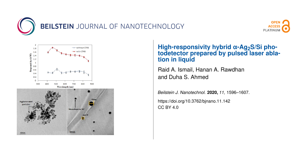
TEM images of the Ag2S NPs synthesized with and without CTAB are shown in Figure 6. The TEM image shown in Figure 6a confirms that the Ag2S particles prepared in pure Tu had a spherical morphology and different sizes due to the agglomeration effect of the high surface energy of the NPs. The surfaces of spherical particles have high-index crystallographic planes, which increase the surface energy of synthesized NPs [35]. The average particle size was approximately 40 ± 5 nm, and the agglomerated particles tended to form large particles. The Ag2S NPs prepared in the mixture of Tu and CTAB were monodisperse NPs with purely spherical shapes, and the average particle size was approximately 30 ± 5 nm. Figure 6b shows monodisperse NPs, which did not agglomerate or aggregate after the CTAB surfactant was added. These observations confirmed the effective capping of CTAB on the Ag2S NP surfaces. The reason for the formation of monodisperse Ag2S NPs when CTAB was used as a surfactant can be ascribed to the deposition of CTAB on the Ag2S NP surface, which resulted in a certain repulsive force to other Ag2S NPs. This force may have prevented the agglomeration of the Ag2S NPs. CTAB has a positive surface charge [36], and CTAB molecules accumulated on the surfaces of the Ag2S NPs and repelled other Ag2S NPs due to the mobile electronic charges in Ag2S (negative surface charge).
![[2190-4286-11-142-6]](/bjnano/content/figures/2190-4286-11-142-6.png?scale=2.0&max-width=1024&background=FFFFFF)
Figure 6: TEM images of Ag2S NPs synthesized (a) without CTAB and (b) with CTAB surfactant.
Figure 6: TEM images of Ag2S NPs synthesized (a) without CTAB and (b) with CTAB surfactant.
The FTIR spectra of the Ag2S NPs prepared with and without the CTAB surfactant measured in the range of 500–4000 cm−1 are shown in Figure 7. The peaks at 541, 640, and 2210 cm−1 were indexed to the characteristic vibration of the Ag–S bond. The peak at 1460 cm−1 can be indexed to C–C stretching vibration, and the peak at 1650 cm−1 belonged to the stretching vibration of the sulfide group. Two peaks appeared at 2842 and 2942 cm−1 in the FTIR spectrum of Ag2S prepared with CTAB. These peaks were attributed to the methylene (–CH2) extension vibration, indicating the adsorption of CTAB on the nanostructure surface. The broad IR peak at 3400 cm−1 is indexed to the presence of adsorbed water molecules [37].
![[2190-4286-11-142-7]](/bjnano/content/figures/2190-4286-11-142-7.png?scale=2.0&max-width=1024&background=FFFFFF)
Figure 7: FTIR spectra of Ag2S NPs prepared without and with CTAB.
Figure 7: FTIR spectra of Ag2S NPs prepared without and with CTAB.
Figure 8 shows the SEM images of Ag2S NPs synthesized without and with CTAB surfactant. The SEM image of Ag2S prepared without CTAB (Figure 8a) shows the formation of agglomerated and aggregated NPs with particle size of 55 nm. The SEM image shown in Figure 8b confirms that when using CTAB surfactant, monodispersed Ag2S nanoparticles can be obtained with an average size of 45 nm with few agglomerated NPs. Figure 9 shows the particle size distribution of Ag2S synthesized without and with CTAB. The particle size of Ag2S NPs ranged from 10 to 70 nm with an average of 55 nm, while the particle distribution of Ag2S NPs prepared with CTAB ranged from 5 to 60 nm with an average of 45 nm. The particle size distribution of Ag2S prepared with CTAB is nearly Gaussian. The particle size distribution improved after adding CTAB, which plays a major role in preventing particle agglomeration [38]. The energy-dispersive X-ray spectra of the Ag2S NPs prepared with and without CTAB are shown in Figure 10.
![[2190-4286-11-142-8]](/bjnano/content/figures/2190-4286-11-142-8.png?scale=2.0&max-width=1024&background=FFFFFF)
Figure 8: SEM images of Ag2S NPs synthesized in pure Tu solution (a) and Tu with CTAB surfactant solution (b).
Figure 8: SEM images of Ag2S NPs synthesized in pure Tu solution (a) and Tu with CTAB surfactant solution (b)....
![[2190-4286-11-142-9]](/bjnano/content/figures/2190-4286-11-142-9.png?scale=2.0&max-width=1024&background=FFFFFF)
Figure 9: Particle size distribution of Ag2S NPs synthesized (a) without and (b) with CTAB.
Figure 9: Particle size distribution of Ag2S NPs synthesized (a) without and (b) with CTAB.
![[2190-4286-11-142-10]](/bjnano/content/figures/2190-4286-11-142-10.png?scale=2.0&max-width=1024&background=FFFFFF)
Figure 10: EDX of Ag2S NPs synthesized in (a) pure Tu and in (b) Tu with CTAB. The inset shows the measured elements.
Figure 10: EDX of Ag2S NPs synthesized in (a) pure Tu and in (b) Tu with CTAB. The inset shows the measured el...
Figure 10 shows that the [Ag]/[S] weight ratio decreased after adding CTAB. CTAB covered the nanoparticles and led to a decreasing ratio between Ag and S. The origin of nitrogen are thiourea traces attached to the Ag2S nanoparticles, while the origin of carbon is CTAB. Hall measurement revealed that the Ag2S had a negative Hall coefficient, indicating that it is an n-type semiconductor. This finding agrees well with [39]. Figure 11 shows the dark I–V characteristics of an n-Ag2S/p-Si heterojunction prepared without and with CTAB under forward and reverse current flow. The forward current flow increased exponentially with bias voltage for the Ag2S/Si heterojunction synthesized in the presence of the CTAB surfactant, indicating the dominance of diffusion current. In the case of the heterojunction prepared without CTAB, the forward current increased linearly with voltage and tended to saturate at a voltage of 8 V due to the effect of series resistance. The forward current increased after adding CTAB due to the reduced electrical resistance of Ag2S. The reverse current of the heterojunction prepared in pure Tu slightly increased with bias voltage, whereas the reverse current of the heterojunction prepared with CTAB did not depend on the bias voltage. These results indicated an enhancement of the junction properties.
![[2190-4286-11-142-11]](/bjnano/content/figures/2190-4286-11-142-11.png?scale=2.0&max-width=1024&background=FFFFFF)
Figure 11: Dark I–V characteristics of n-Ag2S/p-Si heterojunction prepared with and without CTAB. Inset is the semi-logarithmic of forward versus voltage plot.
Figure 11: Dark I–V characteristics of n-Ag2S/p-Si heterojunction prepared with and without CTAB. Inset is the...
The ideality factor (n) of Ag2S/Si was estimated from the semi-logarithmic plot of the forward current as a function of the voltage (inset of Figure 11) using Equation 3:
![[2190-4286-11-142-i3]](/bjnano/content/inline/2190-4286-11-142-i3.svg?max-width=590&scale=1.18182)
where Is is the saturation current of the heterojunction. The value of n for the heterojunctions prepared in Tu and Tu with CTAB was 4 and 2.7, respectively. The value reduction of n after adding CTAB indicated a remarkable improvement in junction characteristics. The value of turn-on voltage of the heterojunctions was estimated and found to be 2.2 and 1.8 V for heterojunctions prepared in pure Tu and with CTAB surfactant, respectively. Decreasing the turn-on voltage after adding the CTAB can be ascribed to a decrease in the electrical resistivity of Ag2S. Figure 12 illustrates the I–V characteristics under illumination of the heterojunctions at reverse bias. The photocurrent of the heterojunction increased from 460 to 1500 μA at 7.5 V after CTAB was added to the Tu solution.
![[2190-4286-11-142-12]](/bjnano/content/figures/2190-4286-11-142-12.png?scale=2.0&max-width=1024&background=FFFFFF)
Figure 12: Effect of CTAB on the I–V characteristics under illumination of the heterojunctions.
Figure 12: Effect of CTAB on the I–V characteristics under illumination of the heterojunctions.
This result can be ascribed to the positive role of CTAB in increasing the depletion layer width and decreasing the e–h recombination process. The calculated on/off ratio at 5 V of the heterojunctions synthesized without and with CTAB was 42 and 517, respectively. The responsivity Rλ of the photodetector represent one of the most important figures of merit of the photodetector and it can be defined as the ratio of photocurrent Iph to the incident light power Ps as shown in the following equation:
![[2190-4286-11-142-i4]](/bjnano/content/inline/2190-4286-11-142-i4.svg?max-width=590&scale=1.18182)
Figure 13 shows the spectral responsivity (Rλ) of Ag2S prepared in the Tu solutions with and without the CTAB surfactant. We observed a response peak at 460 nm, with a responsivity of approximately 1.85 A/W, for the photodetector prepared with CTAB. The responsivity of the photodetector synthesized in pure Tu was 0.64 A/W at 510 nm. The eternal quantum efficiency EQE of the photodetectors prepared without and with CTAB was estimated and found to be 1.5 × 10²% and 4.5 × 10³% at 510 nm, respectively. This significant increase in the responsivity and quantum efficiency of the photodetector after CTAB addition can be ascribed to the widened depletion layer width and increased minority carrier diffusion length as well as to the large surface area. The blue shift in responsivity of the photodetector after adding of the CTAB can be attributed to the increased energy gap of Ag2S NPs. A semi-flat response was observed after 600 nm, and a broad peak was detected at 760 nm.
![[2190-4286-11-142-13]](/bjnano/content/figures/2190-4286-11-142-13.png?scale=2.0&max-width=1024&background=FFFFFF)
Figure 13: Spectral responsivity Ag2S/Si prepared with and without CTAB surfactant.
Figure 13: Spectral responsivity Ag2S/Si prepared with and without CTAB surfactant.
On the basis of these results, we suggest that adding a surfactant, such as cationic CTAB, to Tu solutions decreases the number of recombination centers and thus reduces the possibility of carrier recombination [39]. The obtained responsivity in the visible region for the photodetector prepared with CTAB was higher than that of silicon-based heterojunction photodetectors [40-44]. The specific detectivity D* of the photodetector was estimated using the following Equation 5:
![[2190-4286-11-142-i5]](/bjnano/content/inline/2190-4286-11-142-i5.svg?max-width=590&scale=1.18182)
where A is the area of the photodetector, Δf is the bandwidth and Id is the dark current of the photodetector. The value of detectivity of the photodetector was increased from 0.32 × 10¹² to 2.3 × 10¹² Jones at 510 nm and at bias voltage of 1.8 V. Table 1 lists the main figures of merit of Ag2S NPs/Si photodetectors prepared without and with CTAB and compared to other photodetectors based on silicon heterojunctions. The fabricated photodetector with CTAB has high figures of merit compared to other photodetectors based silicon heterojunctions.
Table 1: Figures of merit of Ag2S/Si photodetector and other silicon heterojunction photodetectors.
| photodetector type | R (A/W) | D* (Jones) | EQE (%) |
|---|---|---|---|
| Ag2SNPs/Si without CTAB* (this work) | 0.64 at 510 nm | 3.2 × 10¹¹ at 510 nm | 1.5 × 10² at 510 nm |
| Ag2SNPs/Si with CTAB* (this work) | 1.85 at 460 nm | 2.3 × 10¹² at 10 nm | 4.5 × 10³ at 510 nm |
| Ag2SQD/Si [45] | 70 μA/W at 1.55 μm | 1011 at 1.55 μm | – |
| CdS/Si [46] | 0.59 mA/W at 1064 nm | 1.3 × 10¹² at 1064 nm | – |
| CdTe/Si [47] | 0.5 at 950 nm | 1.2 × 10¹¹ at 950 nm | 65 at 950 nm |
| CdO/Si [48] | 0.3 at 600 nm | 7 × 10¹¹ at 600 nm | 62 at 600 nm |
| InSb/Si [49] | 0.132 at 635 nm | 1.9 × 10¹² at 635 nm | – |
The main figures of merit of the photodetectors at peak response were investigated after three weeks of storage under ambient conditions (Table 2). There is no significant variation (about 4%) in the values of figures of merit. This indicates that the photodetectors have good environmental stability and they do not need any encapsulation. The photodetector prepared with CTAB exhibits better stability than that prepared in the absence of CTAB. This result is probably due to the high surface activity of the nanoparticles prepared with CTAB.
Table 2: Stability of the photodetectors.
| time of measurements | R (A/W) | D* (Jones) | EQE (%) |
|---|---|---|---|
| immediately | |||
| Ag2S/Si (without CTAB) | 0.64 | 3.2 × 10¹¹ | 1.5 × 10² |
| Ag2S/Si (with CTAB) | 1.8 | 2.3 × 10¹² | 4.5 × 10³ |
| after three weeks | |||
| Ag2S/Si (without CTAB) | 0.62 ± 0.1 | 3 × 10¹¹ ± 0.3 | 1.42 × 10² ± 0.3 |
| Ag2S/Si (with CTAB) | 1.72 ± 0.1 | 2.1 × 10¹² ± 0.2 | 4.2 × 10² ± 0.2 |
The energy band diagram under illumination of the n-Ag2S NPs/p-Si heterojunction prepared in pure Tu is shown in Figure 14. The electron affinity of Ag2S required for the band line-up construction was obtained from reported data [50]. As shown in Figure 12, the photocurrent in the photodetector came from the generated e–h pairs in the depletion region; this process occurred when hν ≥ Eg (Ag2S NPs). As shown in Figure 14, the electrons drifted to Ag2S, and the holes diffused toward the p-Si substrate.
![[2190-4286-11-142-14]](/bjnano/content/figures/2190-4286-11-142-14.png?scale=2.0&max-width=1024&background=FFFFFF)
Figure 14: Illuminated energy band diagram of hybrid n-Ag2S NPs/p-Si heterojunction.
Figure 14: Illuminated energy band diagram of hybrid n-Ag2S NPs/p-Si heterojunction.
Conclusion
In this work, we successfully prepared monodisperse Ag2S NPs by laser ablation of a silver target in a Tu solution with CTAB as a cationic surfactant. The effect of CTAB on the structural, optical and morphological properties of Ag2S NPs was studied. XRD results showed a preferred orientation along the (−121) plane after CTAB was introduced. TEM investigation showed that the average particle size was decreased after adding the CTAB surfactant and monodisperse spherical NPs were observed. Energy-dispersive X-ray confirmed the presence of S and Ag elements. The optical energy gap of Ag2S increased after adding CTAB surfactant from 1.5 to 2 eV. Raman results indicated the presence of Ag–S bonds and the second-order longitudinal optical phonon 2LO mode; their intensity increased when CTAB was added to Tu. FTIR data revealed the presence of a Ag–S bond located at 510 cm−1. The electrical properties of the Ag2S/Si heterojunction were significantly enhanced after the addition of CTAB surfactant. The responsivity of the Ag2S/Si photodetector at 460 nm was increased by a factor of three after CTAB was added. The energy band diagram of Ag2S–Si heterojunction was constructed from optical and electrical results. The photodetectors exhibited good stability, retaining more than 70% of the initial responsivity after storage under ambient conditions for three weeks without any encapsulation. On the basis of these results, the proposed technique is promising and encouraging for the fabrication of inexpensive high-responsivity photodetectors.
References
-
Henglein, A. J. Phys. Chem. 1980, 84, 3461–3467. doi:10.1021/j100462a031
Return to citation in text: [1] -
Majetich, S. A.; Artman, J. O.; McHenry, M. E.; Nuhfer, N. T.; Staley, S. W. Phys. Rev. B 1993, 48, 16845–16848. doi:10.1103/physrevb.48.16845
Return to citation in text: [1] -
Storhoff, J. J.; Elghanian, R.; Mucic, R. C.; Mirkin, C. A.; Letsinger, R. L. J. Am. Chem. Soc. 1998, 120, 1959–1964. doi:10.1021/ja972332i
Return to citation in text: [1] -
Sun, Y.-P.; Riggs, J. E.; Rollins, H. W.; Guduru, R. J. Phys. Chem. B 1999, 103, 77–82. doi:10.1021/jp9835014
Return to citation in text: [1] -
Sharma, R. C.; Chang, Y. A. Bull. Alloy Phase Diagrams 1986, 7, 263–269. doi:10.1007/bf02869003
Return to citation in text: [1] -
Sadovnikov, S. I.; Gusev, A. I.; Rempel, A. A. Superlattices Microstruct. 2015, 83, 35–47. doi:10.1016/j.spmi.2015.03.024
Return to citation in text: [1] -
Kitova, S.; Eneva, J.; Panov, A.; Haefke, H. J. Imaging Sci. Technol. 1994, 38, 484.
Return to citation in text: [1] -
Gao, F.; Lu, Q.; Komarneni, S. Chem. Mater. 2005, 17, 856–860. doi:10.1021/cm048663t
Return to citation in text: [1] -
Yang, T.; Tang, Y.; Liu, L.; Lv, X.; Wang, Q.; Ke, H.; Deng, Y.; Yang, H.; Yang, X.; Liu, G.; Zhao, Y.; Chen, H. ACS Nano 2017, 11, 1848–1857. doi:10.1021/acsnano.6b07866
Return to citation in text: [1] -
Jin, R.; Cao, Y.; Mirkin, C. A.; Kelly, K. L.; Schatz, G. C.; Zheng, J. G. Science 2001, 294, 1901–1903. doi:10.1126/science.1066541
Return to citation in text: [1] -
Ezenwa, I.; Okreke, N. A.; Egwunyenga, N. J. Int. J. Sci. Technol. 2012, 2, 101–106.
Return to citation in text: [1] -
Aleali, H.; Sarkhosh, L.; Karimzadeh, R.; Mansour, N. Phys. Status Solidi B 2011, 248, 680–685. doi:10.1002/pssb.201046107
Return to citation in text: [1] -
Sadovnikov, S. I.; Kuznetsova, Y. V.; Rempel, A. A. Nano-Struct. Nano-Objects 2016, 7, 81–91. doi:10.1016/j.nanoso.2016.06.004
Return to citation in text: [1] -
Chen, M.; Xie, Y.; Chen, H.; Qiao, Z.; Qian, Y. J. Colloid Interface Sci. 2001, 237, 47–53. doi:10.1006/jcis.2001.7436
Return to citation in text: [1] -
Dong, L.; Chu, Y.; Liu, Y.; Li, L. J. Colloid Interface Sci. 2008, 317, 485–492. doi:10.1016/j.jcis.2007.09.055
Return to citation in text: [1] -
Zhang, C.; Zhang, S.; Yu, L.; Zhang, Z.; Zhang, P.; Wu, Z. Mater. Lett. 2012, 85, 77–80. doi:10.1016/j.matlet.2012.06.112
Return to citation in text: [1] -
Kang, M. H.; Kim, S. H.; Jang, S.; Lim, J. E.; Chang, H.; Kong, K.-j.; Myung, S.; Park, J. K. RSC Adv. 2018, 8, 28447–28452. doi:10.1039/c8ra03306d
Return to citation in text: [1] -
Tretyakov, I.; Shurakov, A.; Perepelitsa, A.; Kaurova, N.; Svyatodukh, S.; Zilberley, T.; Ryabchun, S.; Smirnov, M.; Ovchinnikov, O.; Goltsman, G. Phys. Status Solidi RRL 2019, 13, 1900187. doi:10.1002/pssr.201900187
Return to citation in text: [1] -
Slistan-Grijalva, A.; Herrera-Urbina, R.; Rivas-Silva, J. F.; Ávalos-Borja, M.; Castillón-Barraza, F. F.; Posada-Amarillas, A. Phys. E (Amsterdam, Neth.) 2005, 27, 104–112. doi:10.1016/j.physe.2004.10.014
Return to citation in text: [1] -
Ismail, R. A.; Khalaf, W. K.; Abdulrazaq, O. A. Solid-State Electron. 2007, 51, 817–819. doi:10.1016/j.sse.2007.05.011
Return to citation in text: [1] -
Ismail, R. A.; Ahmed, D. S.; Rawdhan, H. A. Mater. Res. Express 2019, 6, 125026. doi:10.1088/2053-1591/ab5348
Return to citation in text: [1] -
Almeida, J. M. P.; Lu, C.; Mendonça, C. R.; Arnold, C. B. Opt. Mater. Express 2015, 5, 1815–1821. doi:10.1364/ome.5.001815
Return to citation in text: [1] -
Sadovnikov, S. I.; Vovkotrub, E. G.; Rempel, A. A. Dokl. Phys. Chem. 2018, 480, 81–84. doi:10.1134/s0012501618060027
Return to citation in text: [1] -
Singh, Z.; Singh, I. Sci. Rep. 2019, 9, 5880. doi:10.1038/s41598-019-42419-z
Return to citation in text: [1] -
Cifuentes, A.; Bernal, J. L.; Diez-Masa, J. C. Anal. Chem. (Washington, DC, U. S.) 1997, 69, 4271–4274. doi:10.1021/ac970696n
Return to citation in text: [1] -
Cui, X.; Yuan, C.; Li, S.; Hu, T.; Bao, J.; Chen, S. Micro Nano Lett. 2017, 12, 714–716. doi:10.1049/mnl.2017.0149
Return to citation in text: [1] -
Fu, X.; Jiang, T.; Zhao, Q.; Yin, H. J. Raman Spectrosc. 2012, 43, 1191–1195. doi:10.1002/jrs.4033
Return to citation in text: [1] -
Alekperov, O.; Jahangirli, Z.; Paucar, R. Phys. Status Solidi B 2016, 253, 2049–2055. doi:10.1002/pssb.201552784
Return to citation in text: [1] -
Shakouri-Arani, M.; Salavati-Niasari, M. Spectrochim. Acta, Part A 2014, 133, 463–471. doi:10.1016/j.saa.2014.05.060
Return to citation in text: [1] -
Mafuné,, F.; Kohno, J.-y.; Takeda, Y.; Kondow, T.; Sawabe, H. J. Phys. Chem. B 2000, 104, 8333–8337. doi:10.1021/jp001803b
Return to citation in text: [1] -
Ortega, E. V.; Berk, D. Ind. Eng. Chem. Res. 2006, 45, 1863–1868. doi:10.1021/ie050516x
Return to citation in text: [1] -
Selvi, S. S. T.; Linet, J. M.; Sagadevan, S. J. Exp. Nanosci. 2018, 13, 130–143. doi:10.1080/17458080.2018.1445306
Return to citation in text: [1] -
Zhao, N.; Qi, L. Adv. Mater. (Weinheim, Ger.) 2006, 18, 359–362. doi:10.1002/adma.200501756
Return to citation in text: [1] -
Sadovnikov, S. I.; Gusev, A. I. J. Mater. Chem. A 2017, 5, 17676–17704. doi:10.1039/c7ta04949h
Return to citation in text: [1] -
Lee, S.-M.; Cho, S.-N.; Cheon, J. Adv. Mater. (Weinheim, Ger.) 2003, 15, 441–444. doi:10.1002/adma.200390102
Return to citation in text: [1] -
Arulraj, A.; Ilayaraja, N.; Rajeshkumar, V.; Ramesh, M. Sci. Rep. 2019, 9, 10108. doi:10.1038/s41598-019-46583-0
Return to citation in text: [1] -
Cava, R. J.; McWhan, D. B. Phys. Rev. Lett. 1980, 45, 2046–2050. doi:10.1103/physrevlett.45.2046
Return to citation in text: [1] -
Díaz-Núñez, P.; González-Izquierdo, J.; González-Rubio, G.; Guerrero-Martínez, A.; Rivera, A.; Perlado, J.; Bañares, L.; Peña-Rodríguez, O. Appl. Sci. 2017, 7, 793. doi:10.3390/app7080793
Return to citation in text: [1] -
Abdi, S.; Dorranian, D. Opt. Laser Technol. 2018, 108, 372–377. doi:10.1016/j.optlastec.2018.07.009
Return to citation in text: [1] [2] -
Zhang, J.; Liu, C.; Zhang, X.; Ke, F.; Han, Y.; Peng, G.; Ma, Y.; Gao, C. Appl. Phys. Lett. 2013, 103, 082116. doi:10.1063/1.4819160
Return to citation in text: [1] -
Chen, D.; Wei, L.; Wang, D.; Chen, Y.; Tian, Y.; Yan, S.; Mei, L.; Jiao, J. J. Alloys Compd. 2018, 735, 2491–2496. doi:10.1016/j.jallcom.2017.11.376
Return to citation in text: [1] -
Abdulnabi, R. K.; Mohsin, M. H.; Ismail, R. A.; Mousa, A. M.; Jawad, M. F. Optik (Munich, Ger.) 2019, 176, 206–213. doi:10.1016/j.ijleo.2018.09.069
Return to citation in text: [1] -
Ismail, R. A.; Hamoudi, W. K.; Saleh, K. K. Mater. Sci. Semicond. Process. 2014, 21, 194–199. doi:10.1016/j.mssp.2013.10.027
Return to citation in text: [1] -
Ismail, R. A.; Mousa, A. M.; Shaker, S. S. Mater. Sci. Semicond. Process. 2019, 99, 165–174. doi:10.1016/j.mssp.2019.04.035
Return to citation in text: [1] -
Tretyakov, I.; Svyatodukh, S.; Perepelitsa, A.; Ryabchun, S.; Kaurova, N.; Shurakov, A.; Smirnov, M.; Ovchinnikov, O.; Goltsman, G. Nanomaterials 2020, 10, 861. doi:10.3390/nano10050861
Return to citation in text: [1] -
Dai, Y.; Wang, X.; Peng, W.; Xu, C.; Wu, C.; Dong, K.; Liu, R.; Wang, Z. L. Adv. Mater. (Weinheim, Ger.) 2018, 30, 1705893. doi:10.1002/adma.201705893
Return to citation in text: [1] -
Ismail, R. A.; Hassan, K. I.; Abdulrazaq, O. A.; Abode, W. H. Mater. Sci. Semicond. Process. 2007, 10, 19–23. doi:10.1016/j.mssp.2006.12.001
Return to citation in text: [1] -
Ismail, R. A.; Al-Samarai, A.-M. E.; Mohmed, S. J.; Ahmed, H. H. Solid-State Electron. 2013, 82, 115–121. doi:10.1016/j.sse.2013.02.035
Return to citation in text: [1] -
Li, X.; Sun, T.; Zhou, K.; Hong, X.; Tang, X.; Wei, D.; Feng, W.; Shen, J.; Wei, D. Nanotechnology 2020, 31, 315204. doi:10.1088/1361-6528/ab884c
Return to citation in text: [1] -
Feng, Y.; Lin, S.; Wen, X.; Zhang, P.; Huang, S.; Shrestha, S.; Green, M.; Conibeer, G. Proc. SPIE 2013, 8923, 89231J. doi:10.1117/12.2033683
Return to citation in text: [1]
| 38. | Díaz-Núñez, P.; González-Izquierdo, J.; González-Rubio, G.; Guerrero-Martínez, A.; Rivera, A.; Perlado, J.; Bañares, L.; Peña-Rodríguez, O. Appl. Sci. 2017, 7, 793. doi:10.3390/app7080793 |
| 39. | Abdi, S.; Dorranian, D. Opt. Laser Technol. 2018, 108, 372–377. doi:10.1016/j.optlastec.2018.07.009 |
| 39. | Abdi, S.; Dorranian, D. Opt. Laser Technol. 2018, 108, 372–377. doi:10.1016/j.optlastec.2018.07.009 |
| 1. | Henglein, A. J. Phys. Chem. 1980, 84, 3461–3467. doi:10.1021/j100462a031 |
| 2. | Majetich, S. A.; Artman, J. O.; McHenry, M. E.; Nuhfer, N. T.; Staley, S. W. Phys. Rev. B 1993, 48, 16845–16848. doi:10.1103/physrevb.48.16845 |
| 3. | Storhoff, J. J.; Elghanian, R.; Mucic, R. C.; Mirkin, C. A.; Letsinger, R. L. J. Am. Chem. Soc. 1998, 120, 1959–1964. doi:10.1021/ja972332i |
| 10. | Jin, R.; Cao, Y.; Mirkin, C. A.; Kelly, K. L.; Schatz, G. C.; Zheng, J. G. Science 2001, 294, 1901–1903. doi:10.1126/science.1066541 |
| 11. | Ezenwa, I.; Okreke, N. A.; Egwunyenga, N. J. Int. J. Sci. Technol. 2012, 2, 101–106. |
| 12. | Aleali, H.; Sarkhosh, L.; Karimzadeh, R.; Mansour, N. Phys. Status Solidi B 2011, 248, 680–685. doi:10.1002/pssb.201046107 |
| 13. | Sadovnikov, S. I.; Kuznetsova, Y. V.; Rempel, A. A. Nano-Struct. Nano-Objects 2016, 7, 81–91. doi:10.1016/j.nanoso.2016.06.004 |
| 23. | Sadovnikov, S. I.; Vovkotrub, E. G.; Rempel, A. A. Dokl. Phys. Chem. 2018, 480, 81–84. doi:10.1134/s0012501618060027 |
| 50. | Feng, Y.; Lin, S.; Wen, X.; Zhang, P.; Huang, S.; Shrestha, S.; Green, M.; Conibeer, G. Proc. SPIE 2013, 8923, 89231J. doi:10.1117/12.2033683 |
| 7. | Kitova, S.; Eneva, J.; Panov, A.; Haefke, H. J. Imaging Sci. Technol. 1994, 38, 484. |
| 8. | Gao, F.; Lu, Q.; Komarneni, S. Chem. Mater. 2005, 17, 856–860. doi:10.1021/cm048663t |
| 9. | Yang, T.; Tang, Y.; Liu, L.; Lv, X.; Wang, Q.; Ke, H.; Deng, Y.; Yang, H.; Yang, X.; Liu, G.; Zhao, Y.; Chen, H. ACS Nano 2017, 11, 1848–1857. doi:10.1021/acsnano.6b07866 |
| 5. | Sharma, R. C.; Chang, Y. A. Bull. Alloy Phase Diagrams 1986, 7, 263–269. doi:10.1007/bf02869003 |
| 6. | Sadovnikov, S. I.; Gusev, A. I.; Rempel, A. A. Superlattices Microstruct. 2015, 83, 35–47. doi:10.1016/j.spmi.2015.03.024 |
| 21. | Ismail, R. A.; Ahmed, D. S.; Rawdhan, H. A. Mater. Res. Express 2019, 6, 125026. doi:10.1088/2053-1591/ab5348 |
| 48. | Ismail, R. A.; Al-Samarai, A.-M. E.; Mohmed, S. J.; Ahmed, H. H. Solid-State Electron. 2013, 82, 115–121. doi:10.1016/j.sse.2013.02.035 |
| 4. | Sun, Y.-P.; Riggs, J. E.; Rollins, H. W.; Guduru, R. J. Phys. Chem. B 1999, 103, 77–82. doi:10.1021/jp9835014 |
| 22. | Almeida, J. M. P.; Lu, C.; Mendonça, C. R.; Arnold, C. B. Opt. Mater. Express 2015, 5, 1815–1821. doi:10.1364/ome.5.001815 |
| 49. | Li, X.; Sun, T.; Zhou, K.; Hong, X.; Tang, X.; Wei, D.; Feng, W.; Shen, J.; Wei, D. Nanotechnology 2020, 31, 315204. doi:10.1088/1361-6528/ab884c |
| 17. | Kang, M. H.; Kim, S. H.; Jang, S.; Lim, J. E.; Chang, H.; Kong, K.-j.; Myung, S.; Park, J. K. RSC Adv. 2018, 8, 28447–28452. doi:10.1039/c8ra03306d |
| 19. | Slistan-Grijalva, A.; Herrera-Urbina, R.; Rivas-Silva, J. F.; Ávalos-Borja, M.; Castillón-Barraza, F. F.; Posada-Amarillas, A. Phys. E (Amsterdam, Neth.) 2005, 27, 104–112. doi:10.1016/j.physe.2004.10.014 |
| 46. | Dai, Y.; Wang, X.; Peng, W.; Xu, C.; Wu, C.; Dong, K.; Liu, R.; Wang, Z. L. Adv. Mater. (Weinheim, Ger.) 2018, 30, 1705893. doi:10.1002/adma.201705893 |
| 16. | Zhang, C.; Zhang, S.; Yu, L.; Zhang, Z.; Zhang, P.; Wu, Z. Mater. Lett. 2012, 85, 77–80. doi:10.1016/j.matlet.2012.06.112 |
| 20. | Ismail, R. A.; Khalaf, W. K.; Abdulrazaq, O. A. Solid-State Electron. 2007, 51, 817–819. doi:10.1016/j.sse.2007.05.011 |
| 47. | Ismail, R. A.; Hassan, K. I.; Abdulrazaq, O. A.; Abode, W. H. Mater. Sci. Semicond. Process. 2007, 10, 19–23. doi:10.1016/j.mssp.2006.12.001 |
| 15. | Dong, L.; Chu, Y.; Liu, Y.; Li, L. J. Colloid Interface Sci. 2008, 317, 485–492. doi:10.1016/j.jcis.2007.09.055 |
| 40. | Zhang, J.; Liu, C.; Zhang, X.; Ke, F.; Han, Y.; Peng, G.; Ma, Y.; Gao, C. Appl. Phys. Lett. 2013, 103, 082116. doi:10.1063/1.4819160 |
| 41. | Chen, D.; Wei, L.; Wang, D.; Chen, Y.; Tian, Y.; Yan, S.; Mei, L.; Jiao, J. J. Alloys Compd. 2018, 735, 2491–2496. doi:10.1016/j.jallcom.2017.11.376 |
| 42. | Abdulnabi, R. K.; Mohsin, M. H.; Ismail, R. A.; Mousa, A. M.; Jawad, M. F. Optik (Munich, Ger.) 2019, 176, 206–213. doi:10.1016/j.ijleo.2018.09.069 |
| 43. | Ismail, R. A.; Hamoudi, W. K.; Saleh, K. K. Mater. Sci. Semicond. Process. 2014, 21, 194–199. doi:10.1016/j.mssp.2013.10.027 |
| 44. | Ismail, R. A.; Mousa, A. M.; Shaker, S. S. Mater. Sci. Semicond. Process. 2019, 99, 165–174. doi:10.1016/j.mssp.2019.04.035 |
| 14. | Chen, M.; Xie, Y.; Chen, H.; Qiao, Z.; Qian, Y. J. Colloid Interface Sci. 2001, 237, 47–53. doi:10.1006/jcis.2001.7436 |
| 18. | Tretyakov, I.; Shurakov, A.; Perepelitsa, A.; Kaurova, N.; Svyatodukh, S.; Zilberley, T.; Ryabchun, S.; Smirnov, M.; Ovchinnikov, O.; Goltsman, G. Phys. Status Solidi RRL 2019, 13, 1900187. doi:10.1002/pssr.201900187 |
| 45. | Tretyakov, I.; Svyatodukh, S.; Perepelitsa, A.; Ryabchun, S.; Kaurova, N.; Shurakov, A.; Smirnov, M.; Ovchinnikov, O.; Goltsman, G. Nanomaterials 2020, 10, 861. doi:10.3390/nano10050861 |
| 29. | Shakouri-Arani, M.; Salavati-Niasari, M. Spectrochim. Acta, Part A 2014, 133, 463–471. doi:10.1016/j.saa.2014.05.060 |
| 25. | Cifuentes, A.; Bernal, J. L.; Diez-Masa, J. C. Anal. Chem. (Washington, DC, U. S.) 1997, 69, 4271–4274. doi:10.1021/ac970696n |
| 26. | Cui, X.; Yuan, C.; Li, S.; Hu, T.; Bao, J.; Chen, S. Micro Nano Lett. 2017, 12, 714–716. doi:10.1049/mnl.2017.0149 |
| 27. | Fu, X.; Jiang, T.; Zhao, Q.; Yin, H. J. Raman Spectrosc. 2012, 43, 1191–1195. doi:10.1002/jrs.4033 |
| 28. | Alekperov, O.; Jahangirli, Z.; Paucar, R. Phys. Status Solidi B 2016, 253, 2049–2055. doi:10.1002/pssb.201552784 |
| 36. | Arulraj, A.; Ilayaraja, N.; Rajeshkumar, V.; Ramesh, M. Sci. Rep. 2019, 9, 10108. doi:10.1038/s41598-019-46583-0 |
| 37. | Cava, R. J.; McWhan, D. B. Phys. Rev. Lett. 1980, 45, 2046–2050. doi:10.1103/physrevlett.45.2046 |
| 34. | Sadovnikov, S. I.; Gusev, A. I. J. Mater. Chem. A 2017, 5, 17676–17704. doi:10.1039/c7ta04949h |
| 35. | Lee, S.-M.; Cho, S.-N.; Cheon, J. Adv. Mater. (Weinheim, Ger.) 2003, 15, 441–444. doi:10.1002/adma.200390102 |
| 32. | Selvi, S. S. T.; Linet, J. M.; Sagadevan, S. J. Exp. Nanosci. 2018, 13, 130–143. doi:10.1080/17458080.2018.1445306 |
| 33. | Zhao, N.; Qi, L. Adv. Mater. (Weinheim, Ger.) 2006, 18, 359–362. doi:10.1002/adma.200501756 |
| 30. | Mafuné,, F.; Kohno, J.-y.; Takeda, Y.; Kondow, T.; Sawabe, H. J. Phys. Chem. B 2000, 104, 8333–8337. doi:10.1021/jp001803b |
| 31. | Ortega, E. V.; Berk, D. Ind. Eng. Chem. Res. 2006, 45, 1863–1868. doi:10.1021/ie050516x |
© 2020 Ismail et al.; licensee Beilstein-Institut.
This is an Open Access article under the terms of the Creative Commons Attribution License (https://creativecommons.org/licenses/by/4.0). Please note that the reuse, redistribution and reproduction in particular requires that the authors and source are credited.
The license is subject to the Beilstein Journal of Nanotechnology terms and conditions: (https://www.beilstein-journals.org/bjnano)