Abstract
We report the superconducting properties of the Co2Cr1−xFexAly/Cu/Ni/Cu/Pb spin-valve structure the magnetic part of which comprises the Heusler alloy layer HA = Co2Cr1−xFexAly with a high degree of spin polarization (DSP) of the conduction band and a Ni layer of variable thickness. The separation between the superconducting transition curves measured for the parallel (α = 0°) and perpendicular (α = 90°) orientation of the magnetization of the HA and the Ni layers reaches up to 0.5 K (α is the angle between the magnetization of two ferromagnetic layers). For all studied samples the dependence of the superconducting transition temperature Tc on α demonstrates a deep minimum in the vicinity of the perpendicular configuration of the magnetizations. This suggests that the observed minimum and the corresponding full switching effect of the spin valve is caused by the long-range triplet component of the superconducting condensate in the multilayer. Such a large effect can be attributed to a half-metallic nature of the HA layer, which in the orthogonal configuration efficiently draws off the spin-polarized Cooper pairs from the space between the HA and Ni layers. Our results indicate a significant potential of the concept of a superconducting spin-valve multilayer comprising a half-metallic ferromagnet, recently proposed by A. Singh et al., Phys. Rev. X 2015, 5, 021019, in achieving large values of the switching effect.
Introduction
For decades, metallic thin-film heterostructures have been in the in the focus of fundamental research in condensed matter physics and materials science. They show novel fundamental physical phenomena that are absent in the initial materials from which the heterostructures are made. Moreover, those phenomena can also be of remarkable technological relevance. A very prominent example is the discovery, in 1988, of the giant magnetoresistance (GMR) effect in heterostructures composed of alternating layers of ferromagnetic and nonmagnetic metallic layers, which opened a new era of electronics, the so-called spin electronics or, in short, spintronics [1-3].
A new, more recent development in spintronics was based on the idea of integrating superconducting layers into the heterostuctures, which gave rise to the field of superconducting (SC) spintronics (for a review see [4]). The so-called superconducting spin valve (SSV) effect that can be used in SC spintronics was proposed theoretically for the first time by Oh et al. [5] and later on by Tagirov [6]. The construction suggested by Oh et al. was an F1/F2/S structure, where F1 and F2 are the ferromagnetic (F) layers and S is the SC layer, whereas Tagirov proposed a different stacking of the layers F1/S/F2. In both cases the “handle” that switches the SC current in the trilayer is the exchange field from two F layers acting on the S layer. This field is larger for the parallel (P) orientation of the magnetization of the F layers (SC is “off”) rather than for their antiparallel (AP) orientation (SC is “on”). Experimentally, the F1/S/F2 structure was realized first. Gu et al. [7] found in the system CuNi/Nb/CuNi a magnitude of the SSV effect ![[Graphic 1]](/bjnano/content/inline/2190-4286-10-144-i3.svg?max-width=637&scale=1.18182) (where
(where ![[Graphic 2]](/bjnano/content/inline/2190-4286-10-144-i4.svg?max-width=637&scale=1.18182) and
and ![[Graphic 3]](/bjnano/content/inline/2190-4286-10-144-i5.svg?max-width=637&scale=1.18182) are the SC transition temperatures for the AP and P orientation of the magnetization of the F1 and the F2 layer) of 6 mK and a width of the SC transition curves δTc≈ 0.1 K. Unfortunately, the full switching between the normal and SC states could not be achieved because the necessary relation between ΔTc and δTc, ΔTc> δTc was by far not fulfilled. Since then much experimental work reviewed in [4,8,9] was done until, in 2010, some of the present authors have demonstrated the full on/off switching between the SC and normal states in a Fe1/Cu/Fe2/In heterostructure, as proposed by Oh et al., with ΔTc = 19 mK and δTc ≈ 7 mK [10]. That the F1/F2/S structure is indeed beneficial in achieving the full SSV effect was previously indicated by the results in [11], in which possible values of ΔTc≈ 200 mK in the superlattice [Fe2V11]20 was obtained indirectly.
are the SC transition temperatures for the AP and P orientation of the magnetization of the F1 and the F2 layer) of 6 mK and a width of the SC transition curves δTc≈ 0.1 K. Unfortunately, the full switching between the normal and SC states could not be achieved because the necessary relation between ΔTc and δTc, ΔTc> δTc was by far not fulfilled. Since then much experimental work reviewed in [4,8,9] was done until, in 2010, some of the present authors have demonstrated the full on/off switching between the SC and normal states in a Fe1/Cu/Fe2/In heterostructure, as proposed by Oh et al., with ΔTc = 19 mK and δTc ≈ 7 mK [10]. That the F1/F2/S structure is indeed beneficial in achieving the full SSV effect was previously indicated by the results in [11], in which possible values of ΔTc≈ 200 mK in the superlattice [Fe2V11]20 was obtained indirectly.
Another very remarkable advantage of the F1/F2/S system is its functionality as an SC triplet spin valve theoretically predicted by Fominov and co-workers [12]. It is related to the generation of the long-range triplet component (LRTC) of the SC condensate at noncollinear orientations of the magnetization of the F1 and the F2 layer and yields a minimum of the SC critical temperature Tc of the system in an approximately orthogonal geometry. This theoretical prediction was experimentally confirmed for the first time by some of us in the study of the Fe1/Cu/Fe2/Pb multilayer [13]. A constantly growing experimental and theoretical interest to the various aspects of the LRTC and its implications for the functionality of SSVs has evolved by now into a new area in the field of SC spintronics [4,8,9].
Recently, Singh et al. [14] have reported a record value of ![[Graphic 4]](/bjnano/content/inline/2190-4286-10-144-i6.svg?max-width=637&scale=1.18182) = 0.6–0.8 K due to LRTC in the CrO2/Cu/Ni/MoGe heterostructure where one of the F layers was made of the half-metallic compound CrO2.
= 0.6–0.8 K due to LRTC in the CrO2/Cu/Ni/MoGe heterostructure where one of the F layers was made of the half-metallic compound CrO2. ![[Graphic 5]](/bjnano/content/inline/2190-4286-10-144-i7.svg?max-width=637&scale=1.18182) = Tc(α = 0°) − Tc(α = 90°) and α is the angle between the directions of the magnetization of the two F layers. The reason for the large effect was attributed to the efficiency of the half-metallic CrO2 layer in drawing off the spin-polarized Cooper pairs from the space between the two F layers.
= Tc(α = 0°) − Tc(α = 90°) and α is the angle between the directions of the magnetization of the two F layers. The reason for the large effect was attributed to the efficiency of the half-metallic CrO2 layer in drawing off the spin-polarized Cooper pairs from the space between the two F layers.
The goals of the present work were twofold. First, we considered it necessary to verify the breakthrough results by Singh et al. [14], and, second, which was even more important, to answer the question whether the proposed concept of the SSV with a half-metallic F element is of a general character. That is, to find out whether a large SSV effect can be realized using materials other than CrO2 in the magnetic part and other than MoGe in the superconducting part of the SSV. Indeed, as will be shown below, we could verify and generalize the results of the pioneering work by Singh and co-workers [14]. Previously, we have shown the advantages of using the Heusler alloy (HA) Co2Cr1−xFexAly as a weak ferromagnet in the F2 layer of the F1/F2/S SSV structure [15]. Therefore, instead of CrO2, which in accordance with the data on point contact spectroscopy [16], has a 90% polarization of the conduction band, we have chosen as a drawing layer for LRTC the HA Co2Cr1−xFexAly with a spin polarization of the conduction band of ≥70% [17] and instead of MoGe as an S layer we have used the elemental superconductor Pb.
Sample Preparation and Experimental Results
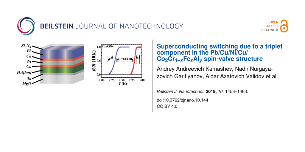
We prepared several sets of the F1/F2/S spin-valve structures containing HA = Co2Cr1−xFexAly with the high degree of spin polarization (DSP) of the conduction band standing for the F1 layer adapting the preparation method from [17]. The grown heterostructures have the following composition: MgO/Ta(5 nm)/HA(20 nm)/Cu(4 nm)/Ni(dNi)/Cu(1.5 nm)/Pb(105 nm)/Si3N4 with the variable Ni layer thickness, dNi, in the range from 0.6 to 2.5 nm. In this construction MgO(001) is a high-quality single crystalline substrate, Ta(5 nm) is a buffer layer necessary for the optimal growth of the whole structure, HA and Ni play the roles of the ferromagnetic F1 and F2 layer, respectively, Cu(4 nm) decouples the magnetization of the F1 and the F2 layer, Pb(105 nm) is an S layer, Si3N4 is a protective layer against oxidation, and Cu(1.5 nm) is a buffer layer necessary for the optimal growth of the Pb layer. The Ni, Cu and Pb layers were prepared using e-beam techniques. For the fabrication of the HA and the Si3N4 layers dc sputtering was used. We used deposition rates of 0.4 Å/s for HA and Si3N4, 0.5 Å/s for Cu and Ni, and 10 Å/s for Pb. At first, when evaporating HA, the substrate temperature was kept at Tsub = 700 K to achieve the desired spin polarization of the conduction band of the HA. Indeed, in accordance with our previous work [17] the composition of our alloy, which we call a Heusler alloy, is, in reality, Co2Cr1−xFexAl0.63 with x = 0.48. Obviously, there is deficiency of aluminum in this compound in comparison with the ideal Heusler composition Co2Cr1−xFexAly. In fact, this “not ideal” composition demonstrates a high DSP of the order of 70% [17]. The study by S. Husain et al. [18] shows that the DSP increases with increasing the substrate temperature Tsub. Therefore, we expect the DSP in our samples to be of the order of 80%. According to our previous study [19], in order to improve the smoothness of the Pb layer the substrate temperature should be reduced down to Tsub≈ 150 K. Therefore, the top Cu(4 nm)/Ni(dNi)/Cu(1.5 nm)/Pb fragment was grown at this reduced Tsub. Finally, all samples were covered with a protective Si3N4 layer to prevent oxidation of the Pb layer.
The Ni layer with the thickness dNi≤ 2 nm has coercive field of the order of 2 kOe [20]. In the present study the Ni layer is deposited at a substrate temperature of Tsub≈ 150 K. Therefore its coercive field should be even larger because the density of dislocation increases with decreasing Tsub.
As to the HA layer, our SQUID magnetization measurements show that the onset of the saturation of its magnetization occurs at 30 Oe. At higher magnetic fields the magnetization continues to increase slightly up to the magnetic field of 3 kOe possibly due to some magnetic inhomogeneity of the HA layer. We note that the magnetic response from the Ni layer cannot be resolved here due to its small value.
The electrical resistivity was measured using the standard four-point method. The top insulating layer (Si3N4) was mechanically removed from the areas where the golden wires should be attached using a silver paste. The quality of the Pb layer can be judged from the residual resistivity ratio (RRR):
![[Graphic 6]](/bjnano/content/inline/2190-4286-10-144-i8.svg?max-width=637&scale=1.18182)
Here, R(T) is the measured resistance at a given temperature T, ρph(300 K) is the phonon contribution to the specific resistivity at 300 K, and ρ(10 K) is the residual resistivity at 10 K (i.e., above Tc). For our samples this ratio amounted to RRR = 10–12, which corresponds to a SC coherence length of ξS = 41–45 nm (for details see [21]). The critical temperature Tc is defined as the midpoint of the SC transition curve. Its width in zero magnetic field varied from 20 to 50 mK depending on the particular series of the samples and increased with the applied field up to ca. 250 mK (see Figure 2 below). The narrow SC transition is a characteristic feature of the high-quality Pb layer.
For the optimal operation of the SSV it is important to find the optimal thickness of the Pb layer dPb. It needs to be sufficiently small to make the whole S layer sensitive to the magnetic part of the system. Only in this case the mutual orientation of the magnetization of the F1 and the F2 layer would affect the Tc of the stack. In order to determine the optimal thickness we measured the dependence of Tc on dPb for the heterostructure MgO/Ta(5 nm)/Ni(5 nm)/Cu(1.5 nm)/Pb(dPb)/Si3N4. Figure 1 shows the Tc(dPb) dependence for a fixed thickness of the Ni layer dNi = 5 nm, which is much larger than the penetration depth of the Cooper pairs in the Ni layer. The value Tc decreases rapidly when the thickness of the Pb layer dPb is reduced down to 100 nm. For dPb ≤ 90 nm, values of Tc ≤ 1.5 K were obtained. Therefore, the optimal thickness range of the Pb layer lies between 90 and 110 nm and for the further study of the SSV effect we have chosen dPb = 105 nm.
![[2190-4286-10-144-1]](/bjnano/content/figures/2190-4286-10-144-1.png?scale=2.0&max-width=1024&background=FFFFFF)
Figure 1: SC critical temperature Tc as a function of the thickness of the Pb layer dPb at a fixed thickness of the Ni layer dNi = 5 nm for the trilayer Ni(5 nm)/Cu(1.5 nm)/Pb. Solid line is the theoretical fit according to [12] with the coherence length of the Pb layer of ξS = 41 nm.
Figure 1: SC critical temperature Tc as a function of the thickness of the Pb layer dPb at a fixed thickness ...
Moreover, this procedure is standard for a simple estimation of the boundary parameters. In particular, it enables to determine the critical thickness of the SC layer below which superconductivity vanishes ![[Graphic 7]](/bjnano/content/inline/2190-4286-10-144-i9.svg?max-width=637&scale=1.18182) . From this we obtain, in accordance with the Appendix in [22], the transparency parameter of the S/F2 interface
. From this we obtain, in accordance with the Appendix in [22], the transparency parameter of the S/F2 interface ![[Graphic 8]](/bjnano/content/inline/2190-4286-10-144-i10.svg?max-width=637&scale=1.18182) .
.
For the measurements of the angular dependence of Tc in the prepared SSV multilayers we have fixed the magnetization of the F2 layer (Ni) in a certain direction by cooling the sample in a magnetic field down to the operational temperatures of the SSV. The magnetization of the F1 layer (HA) can still be easily rotated by an angle α with respect to the pinned magnetization of the Ni layer by an external in-plane field. To manipulate the magnetization direction of the HA layer a magnetic field of 30 Oe is sufficient. We performed such experiments and find a disappointingly small SSV effect. Then, just for curiosity, we extended our study to higher magnetic fields. Surprisingly, we found that with increasing the magnetic field the triplet contribution to the SSV effect linearly increases with the magnetic field. For example, for the sample PLAK4216 ![[Graphic 9]](/bjnano/content/inline/2190-4286-10-144-i11.svg?max-width=637&scale=1.18182) increases linearly up to 0.4 K at 2 kOe (see Figure 4 below).
increases linearly up to 0.4 K at 2 kOe (see Figure 4 below).
Figure 2 shows the SC transition curves for three representative samples. The shift of the curves between the P (α = 0) and the perpendicular (PP) (α = 90°) orientation, ![[Graphic 10]](/bjnano/content/inline/2190-4286-10-144-i12.svg?max-width=637&scale=1.18182) , varies between 0.18 and 0.51 K.
, varies between 0.18 and 0.51 K.
![[2190-4286-10-144-2]](/bjnano/content/figures/2190-4286-10-144-2.png?scale=2.0&max-width=1024&background=FFFFFF)
Figure 2: SC transition curves for the P and PP configuration of the cooling field used to fix the direction of the magnetization of the Ni layer and the applied magnetic field H0, which rotates the magnetization of the HA layer: (a) sample PLAK4212 at H0 = 2 kOe; (b) sample PLAK4214 at H0 = 2.5 kOe; (c) sample PLAK4216 at H0 = 3.5 kOe.
Figure 2: SC transition curves for the P and PP configuration of the cooling field used to fix the direction ...
Figure 3 depicts the dependence of Tc on α for the sample PLAK4216. It appears qualitatively similar to the ones observed by us previously ([9,13,15,21,23-26]), reaching a minimum near α = 90°. However, the minimum that we observe now is much deeper, suggesting that the SSV effect is dominated by the spin polarized (triplet) Cooper pairs. The main parameters of the studied SSV samples are listed in Table 1.
![[2190-4286-10-144-3]](/bjnano/content/figures/2190-4286-10-144-3.png?scale=2.0&max-width=1024&background=FFFFFF)
Figure 3: Dependence of Tc on the angle α between the direction of the cooling field used to fix the direction of the magnetization of the Ni layer and the applied magnetic field H0 =2 kOe, which rotates the magnetization of the HA layer for sample PLAK4216 HA(20 nm)/Cu(4 nm)/Ni(2.5 nm)/Cu(1.5 nm)/Pb(105 nm). The solid line is the theoretical curve with the parameters presented in section “Discussion”.
Figure 3: Dependence of Tc on the angle α between the direction of the cooling field used to fix the directio...
Table 1:
Parameters of all studied samples with variable Ni layer thickness dNi. ![[Graphic 11]](/bjnano/content/inline/2190-4286-10-144-i13.svg?max-width=637&scale=1.18182) is the maximum value of the triplet SSV effect as determined from the angular dependence Tc(α) obtained at the field H0.
is the maximum value of the triplet SSV effect as determined from the angular dependence Tc(α) obtained at the field H0.
| sample | dNi, nm | ΔTctrip, K | H0, kOe |
|---|---|---|---|
| PLAK4211 | 0.6 | 0.05 | 1.0 |
| PLAK4212 | 0.9 | 0.23 | 2.0 |
| PLAK4213 | 1.3 | 0.13 | 2.0 |
| PLAK4214 | 1.6 | 0.18 | 2.5 |
| PLAK4215 | 2 | 0.05 | 1.25 |
| PLAK4216 | 2.5 | 0.51 | 3.5 |
The magnitude of the triplet SSV effect ![[Graphic 12]](/bjnano/content/inline/2190-4286-10-144-i14.svg?max-width=637&scale=1.18182) depends practically linearly on H at small applied magnetic fields up to the field H0 the values of which are listed in Table 1 together with the corresponding values of
depends practically linearly on H at small applied magnetic fields up to the field H0 the values of which are listed in Table 1 together with the corresponding values of ![[Graphic 13]](/bjnano/content/inline/2190-4286-10-144-i15.svg?max-width=637&scale=1.18182) .
.
At first glance it is surprising that ![[Graphic 14]](/bjnano/content/inline/2190-4286-10-144-i16.svg?max-width=637&scale=1.18182) increases well above the saturation magnetic field for the HA layer. We suppose this may be caused by some magnetic inhomogeneity of the HA layer reflected in a slight increase of its magnetization up to the field of 3 kOe, where more and more “microdomains” become gradually involved in the formation of the total moment. Figure 4 shows the dependence of the triplet contribution to the SSV effect on the external magnetic field for the sample PLAK4216. A similar increase of
increases well above the saturation magnetic field for the HA layer. We suppose this may be caused by some magnetic inhomogeneity of the HA layer reflected in a slight increase of its magnetization up to the field of 3 kOe, where more and more “microdomains” become gradually involved in the formation of the total moment. Figure 4 shows the dependence of the triplet contribution to the SSV effect on the external magnetic field for the sample PLAK4216. A similar increase of ![[Graphic 15]](/bjnano/content/inline/2190-4286-10-144-i17.svg?max-width=637&scale=1.18182) was observed by Singh et al. [14], for which no conclusive explanation can be found at present. This field-dependent effect observed by two groups on different samples appears to be a salient feature of the new type of SSVs and needs theoretical explanation.
was observed by Singh et al. [14], for which no conclusive explanation can be found at present. This field-dependent effect observed by two groups on different samples appears to be a salient feature of the new type of SSVs and needs theoretical explanation.
![[2190-4286-10-144-4]](/bjnano/content/figures/2190-4286-10-144-4.png?scale=2.0&max-width=1024&background=FFFFFF)
Figure 4: The magnitude of the triplet SSV as a function of the applied magnetic field for sample PLAK4216. The line is a guide to the eyes.
Figure 4: The magnitude of the triplet SSV as a function of the applied magnetic field for sample PLAK4216. T...
Discussion
A remarkably large separation of the SC transition curves for the P and the PP orientation of the magnetization of the F1 and the F2 layer yielding values of ![[Graphic 16]](/bjnano/content/inline/2190-4286-10-144-i18.svg?max-width=637&scale=1.18182) up to 0.5 K in not too strong magnetic fields compared to those in [14] evidences prominent spin–triplet superconducting correlations in our samples. The theoretical approach that we employ for the analysis of the experiment in Figure 3 is based on a generalization of [12] along the lines of [27,28]. It allows to consider layered structures with different material parameters of all the layers and arbitrary Kupriyanov–Lukichev boundary parameters [29] of all the interfaces.
up to 0.5 K in not too strong magnetic fields compared to those in [14] evidences prominent spin–triplet superconducting correlations in our samples. The theoretical approach that we employ for the analysis of the experiment in Figure 3 is based on a generalization of [12] along the lines of [27,28]. It allows to consider layered structures with different material parameters of all the layers and arbitrary Kupriyanov–Lukichev boundary parameters [29] of all the interfaces.
Each of the two interfaces (F/S and F/F) is described by the matching parameter γ and the resistance parameter γb [27]:
![[2190-4286-10-144-i1]](/bjnano/content/inline/2190-4286-10-144-i1.svg?max-width=590&scale=1.18182)
![[2190-4286-10-144-i2]](/bjnano/content/inline/2190-4286-10-144-i2.svg?max-width=590&scale=1.18182)
Here, ρ and ξ are the resistance and the coherence length of the layers, Rb and ![[Graphic 17]](/bjnano/content/inline/2190-4286-10-144-i19.svg?max-width=637&scale=1.18182) are the interface resistance and area. The necessity to consider arbitrary F/F interface parameters is due to different materials of the two F layers. This is a new theoretical ingredient, in comparison to fittings of our previous experiments in [9,13,21]. Figure 3 demonstrates that theory correctly reproduces characteristic features of the Tc(α) dependence (triplet spin-valve behavior). Parameters used for fitting of the theory to the experimental results are the following: coherence length in the S-layer, ξS = 41 nm, coherence lengths in the F2 and the F1-layer, ξF2 = 6.25 nm and ξF1 = 40 nm. The boundary conditions of the S/F and F/F interfaces are given by the material matching parameter γ and the transparency parameter γb, γSF = 0.1,
are the interface resistance and area. The necessity to consider arbitrary F/F interface parameters is due to different materials of the two F layers. This is a new theoretical ingredient, in comparison to fittings of our previous experiments in [9,13,21]. Figure 3 demonstrates that theory correctly reproduces characteristic features of the Tc(α) dependence (triplet spin-valve behavior). Parameters used for fitting of the theory to the experimental results are the following: coherence length in the S-layer, ξS = 41 nm, coherence lengths in the F2 and the F1-layer, ξF2 = 6.25 nm and ξF1 = 40 nm. The boundary conditions of the S/F and F/F interfaces are given by the material matching parameter γ and the transparency parameter γb, γSF = 0.1, ![[Graphic 18]](/bjnano/content/inline/2190-4286-10-144-i20.svg?max-width=637&scale=1.18182) , γFF = 1, and
, γFF = 1, and ![[Graphic 19]](/bjnano/content/inline/2190-4286-10-144-i21.svg?max-width=637&scale=1.18182) . The exchange energy of the F1 and of the F2 layer is h2 = 0.03 eV and h1 = 0.39 eV, respectively.
. The exchange energy of the F1 and of the F2 layer is h2 = 0.03 eV and h1 = 0.39 eV, respectively.
Conclusion
When studying the SSV multilayers Co2Cr1−xFexAly/Cu/Ni/Cu/Pb the magnetic part of which contains the Heusler alloy Co2Cr1−xFexAly with a high degree of spin polarization of the conduction band we have obtained a large SSV effect due to the long-range triplet component of the superconducting condensate ![[Graphic 20]](/bjnano/content/inline/2190-4286-10-144-i22.svg?max-width=637&scale=1.18182) ≈ 0.5 K at a moderate applied field of 3.5 kOe as compared with the earlier work in [14]. Our results show that there is a potential to achieve large values of
≈ 0.5 K at a moderate applied field of 3.5 kOe as compared with the earlier work in [14]. Our results show that there is a potential to achieve large values of ![[Graphic 21]](/bjnano/content/inline/2190-4286-10-144-i23.svg?max-width=637&scale=1.18182) even at smaller fields relevant for applications by careful design and optimization of all elements of the SSV heterostructure regarding both the superconducting and the magnetic part. Our observations suggest that the concept of a SSV with a half-metallic ferromagnetic element proposed in [14] is of general character. In particular, finding for this purpose the most appropriate ferromagnet with a high degree of spin polarization of the conduction band appears to be a crucial issue. Furthermore, noting first theoretical attempts in [30,31], our data as well as the results by Singh et al. [14] call for a comprehensive quantitative theoretical treatment to obtain further insights into exciting physics of the triplet superconducting spin valves.
even at smaller fields relevant for applications by careful design and optimization of all elements of the SSV heterostructure regarding both the superconducting and the magnetic part. Our observations suggest that the concept of a SSV with a half-metallic ferromagnetic element proposed in [14] is of general character. In particular, finding for this purpose the most appropriate ferromagnet with a high degree of spin polarization of the conduction band appears to be a crucial issue. Furthermore, noting first theoretical attempts in [30,31], our data as well as the results by Singh et al. [14] call for a comprehensive quantitative theoretical treatment to obtain further insights into exciting physics of the triplet superconducting spin valves.
References
-
Baibich, M. N.; Broto, J. M.; Fert, A.; Van Dau, F. N.; Petroff, F.; Etienne, P.; Creuzet, G.; Friederich, A.; Chazelas, J. Phys. Rev. Lett. 1988, 61, 2472–2475. doi:10.1103/physrevlett.61.2472
Return to citation in text: [1] -
Binasch, G.; Grünberg, P.; Saurenbach, F.; Zinn, W. Phys. Rev. B 1989, 39, 4828–4830. doi:10.1103/physrevb.39.4828
Return to citation in text: [1] -
Prinz, G. A. Science 1998, 282, 1660–1663. doi:10.1126/science.282.5394.1660
Return to citation in text: [1] -
Linder, J.; Robinson, J. W. A. Nat. Phys. 2015, 11, 307–315. doi:10.1038/nphys3242
Return to citation in text: [1] [2] [3] -
Oh, S.; Youm, D.; Beasley, M. R. Appl. Phys. Lett. 1997, 71, 2376–2378. doi:10.1063/1.120032
Return to citation in text: [1] -
Tagirov, L. R. Phys. Rev. Lett. 1999, 83, 2058–2061. doi:10.1103/physrevlett.83.2058
Return to citation in text: [1] -
Gu, J. Y.; You, C.-Y.; Jiang, J. S.; Pearson, J.; Bazaliy, Y. B.; Bader, S. D. Phys. Rev. Lett. 2002, 89, 267001. doi:10.1103/physrevlett.89.267001
Return to citation in text: [1] -
Blamire, M. G.; Robinson, J. W. A. J. Phys.: Condens. Matter 2014, 26, 453201. doi:10.1088/0953-8984/26/45/453201
Return to citation in text: [1] [2] -
Garifullin, I. A.; Leksin, P. V.; Garif׳yanov, N. N.; Kamashev, A. A.; Fominov, Y. V.; Schumann, J.; Krupskaya, Y.; Kataev, V.; Schmidt, O. G.; Büchner, B. J. Magn. Magn. Mater. 2015, 373, 18–22. doi:10.1016/j.jmmm.2014.04.002
Return to citation in text: [1] [2] [3] [4] -
Leksin, P. V.; Garif’yanov, N. N.; Garifullin, I. A.; Schumann, J.; Vinzelberg, H.; Kataev, V.; Klingeler, R.; Schmidt, O. G.; Büchner, B. Appl. Phys. Lett. 2010, 97, 102505. doi:10.1063/1.3486687
Return to citation in text: [1] -
Westerholt, K.; Sprungmann, D.; Zabel, H.; Brucas, R.; Hjörvarsson, B.; Tikhonov, D. A.; Garifullin, I. A. Phys. Rev. Lett. 2005, 95, 097003. doi:10.1103/physrevlett.95.097003
Return to citation in text: [1] -
Fominov, Y. V.; Golubov, A. A.; Karminskaya, T. Y.; Kupriyanov, M. Y.; Deminov, R. G.; Tagirov, L. R. JETP Lett. 2010, 91, 308–313. doi:10.1134/s002136401006010x
Return to citation in text: [1] [2] [3] -
Leksin, P. V.; Garif’yanov, N. N.; Garifullin, I. A.; Fominov, Y. V.; Schumann, J.; Krupskaya, Y.; Kataev, V.; Schmidt, O. G.; Büchner, B. Phys. Rev. Lett. 2012, 109, 057005. doi:10.1103/physrevlett.109.057005
Return to citation in text: [1] [2] [3] -
Singh, A.; Voltan, S.; Lahabi, K.; Aarts, J. Phys. Rev. X 2015, 5, 021019. doi:10.1103/physrevx.5.021019
Return to citation in text: [1] [2] [3] [4] [5] [6] [7] [8] -
Kamashev, A. A.; Leksin, P. V.; Garif’yanov, N. N.; Validov, A. A.; Schumann, J.; Kataev, V.; Büchner, B.; Garifullin, I. A. J. Magn. Magn. Mater. 2018, 459, 7–11. doi:10.1016/j.jmmm.2018.01.085
Return to citation in text: [1] [2] -
Soulen, R.; Byers, J.; Osofsky, M.; Nadgorny, B.; Ambrose, T.; Cheng, S.; Broussard, P.; Tanaka, C.; Nowak, J.; Moodera, J.; Barry, A.; Coey, J. Science 1998, 282, 85–88. doi:10.1126/science.282.5386.85
Return to citation in text: [1] -
Kamashev, A. A.; Leksin, P. V.; Schumann, J.; Kataev, V.; Thomas, J.; Gemming, T.; Büchner, B.; Garifullin, I. A. Phys. Rev. B 2017, 96, 024512. doi:10.1103/physrevb.96.024512
Return to citation in text: [1] [2] [3] [4] -
Husain, S.; Akansel, S.; Kumar, A.; Svedlindh, P.; Chaudhary, S. Sci. Rep. 2016, 6, 28692. doi:10.1038/srep28692
Return to citation in text: [1] -
Leksin, P. V.; Kamashev, A. A.; Schumann, J.; Kataev, V. E.; Thomas, J.; Büchner, B.; Garifullin, I. A. Nano Res. 2016, 9, 1005–1011. doi:10.1007/s12274-016-0988-y
Return to citation in text: [1] -
Leksin, P. V.; Salikhov, R. I.; Garifullin, I. A.; Vinzelberg, H.; Kataev, V.; Klingeler, R.; Tagirov, L. R.; Büchner, B. JETP Lett. 2009, 90, 59–63. doi:10.1134/s0021364009130128
Return to citation in text: [1] -
Leksin, P. V.; Garif'yanov, N. N.; Kamashev, A. A.; Fominov, Y. V.; Schumann, J.; Hess, C.; Kataev, V.; Büchner, B.; Garifullin, I. A. Phys. Rev. B 2015, 91, 214508. doi:10.1103/physrevb.91.214508
Return to citation in text: [1] [2] [3] -
Fominov, Y. V.; Chtchelkatchev, N. M.; Golubov, A. A. Phys. Rev. B 2002, 66, 014507. doi:10.1103/physrevb.66.014507
Return to citation in text: [1] -
Garifullin, I. A.; Garif’yanov, N. N.; Leksin, P. V.; Kamashev, A. A.; Fominov, Y. V.; Schumann, J.; Kataev, V.; Büchner, B. Bull. Russ. Acad. Sci.: Phys. 2014, 78, 1341–1347. doi:10.3103/s1062873814120077
Return to citation in text: [1] -
Garifullin, I.; Garif’yanov, N.; Leksin, P.; Kamashev, A.; Fominov, Y.; Schumann, J.; Kataev, V.; Büchner, B. Magn. Reson. Solids 2014, 16, 14208.
Return to citation in text: [1] -
Leksin, P. V.; Kamashev, A. A.; Garif’yanov, N. N.; Validov, A. A.; Fominov, Y. V.; Schumann, J.; Kataev, V. E.; Büchner, B.; Garifullin, I. A. Phys. Solid State 2016, 58, 2165–2176. doi:10.1134/s1063783416110214
Return to citation in text: [1] -
Leksin, P. V.; Garif'yanov, N. N.; Kamashev, A. A.; Validov, A. A.; Fominov, Y. V.; Schumann, J.; Kataev, V.; Thomas, J.; Büchner, B.; Garifullin, I. A. Phys. Rev. B 2016, 93, 100502. doi:10.1103/physrevb.93.100502
Return to citation in text: [1] -
Deminov, R. G.; Tagirov, L. R.; Gaifullin, R. R.; Karminskaya, T. Y.; Kupriyanov, M. Y.; Fominov, Y. V.; Golubov, A. A. J. Magn. Magn. Mater. 2015, 373, 16–17. doi:10.1016/j.jmmm.2014.02.033
Return to citation in text: [1] [2] -
Deminov, R. G.; Tagirov, L. R.; Gaifullin, R. R.; Fominov, Y. V.; Karminskaya, T. Y.; Kupriyanov, M. Y.; Golubov, A. A. Solid State Phenom. 2015, 233–234, 745–749. doi:10.4028/www.scientific.net/ssp.233-234.745
Return to citation in text: [1] -
Kuprianov, M. Y.; Lukichev, V. F. Sov. Phys. - JETP 1988, 67, 1163.
Return to citation in text: [1] -
Mironov, S.; Buzdin, A. Phys. Rev. B 2015, 92, 184506. doi:10.1103/physrevb.92.184506
Return to citation in text: [1] -
Halterman, K.; Alidoust, M. Phys. Rev. B 2016, 94, 064503. doi:10.1103/physrevb.94.064503
Return to citation in text: [1]
| 14. | Singh, A.; Voltan, S.; Lahabi, K.; Aarts, J. Phys. Rev. X 2015, 5, 021019. doi:10.1103/physrevx.5.021019 |
| 14. | Singh, A.; Voltan, S.; Lahabi, K.; Aarts, J. Phys. Rev. X 2015, 5, 021019. doi:10.1103/physrevx.5.021019 |
| 12. | Fominov, Y. V.; Golubov, A. A.; Karminskaya, T. Y.; Kupriyanov, M. Y.; Deminov, R. G.; Tagirov, L. R. JETP Lett. 2010, 91, 308–313. doi:10.1134/s002136401006010x |
| 1. | Baibich, M. N.; Broto, J. M.; Fert, A.; Van Dau, F. N.; Petroff, F.; Etienne, P.; Creuzet, G.; Friederich, A.; Chazelas, J. Phys. Rev. Lett. 1988, 61, 2472–2475. doi:10.1103/physrevlett.61.2472 |
| 2. | Binasch, G.; Grünberg, P.; Saurenbach, F.; Zinn, W. Phys. Rev. B 1989, 39, 4828–4830. doi:10.1103/physrevb.39.4828 |
| 3. | Prinz, G. A. Science 1998, 282, 1660–1663. doi:10.1126/science.282.5394.1660 |
| 7. | Gu, J. Y.; You, C.-Y.; Jiang, J. S.; Pearson, J.; Bazaliy, Y. B.; Bader, S. D. Phys. Rev. Lett. 2002, 89, 267001. doi:10.1103/physrevlett.89.267001 |
| 15. | Kamashev, A. A.; Leksin, P. V.; Garif’yanov, N. N.; Validov, A. A.; Schumann, J.; Kataev, V.; Büchner, B.; Garifullin, I. A. J. Magn. Magn. Mater. 2018, 459, 7–11. doi:10.1016/j.jmmm.2018.01.085 |
| 30. | Mironov, S.; Buzdin, A. Phys. Rev. B 2015, 92, 184506. doi:10.1103/physrevb.92.184506 |
| 31. | Halterman, K.; Alidoust, M. Phys. Rev. B 2016, 94, 064503. doi:10.1103/physrevb.94.064503 |
| 6. | Tagirov, L. R. Phys. Rev. Lett. 1999, 83, 2058–2061. doi:10.1103/physrevlett.83.2058 |
| 16. | Soulen, R.; Byers, J.; Osofsky, M.; Nadgorny, B.; Ambrose, T.; Cheng, S.; Broussard, P.; Tanaka, C.; Nowak, J.; Moodera, J.; Barry, A.; Coey, J. Science 1998, 282, 85–88. doi:10.1126/science.282.5386.85 |
| 14. | Singh, A.; Voltan, S.; Lahabi, K.; Aarts, J. Phys. Rev. X 2015, 5, 021019. doi:10.1103/physrevx.5.021019 |
| 5. | Oh, S.; Youm, D.; Beasley, M. R. Appl. Phys. Lett. 1997, 71, 2376–2378. doi:10.1063/1.120032 |
| 14. | Singh, A.; Voltan, S.; Lahabi, K.; Aarts, J. Phys. Rev. X 2015, 5, 021019. doi:10.1103/physrevx.5.021019 |
| 14. | Singh, A.; Voltan, S.; Lahabi, K.; Aarts, J. Phys. Rev. X 2015, 5, 021019. doi:10.1103/physrevx.5.021019 |
| 4. | Linder, J.; Robinson, J. W. A. Nat. Phys. 2015, 11, 307–315. doi:10.1038/nphys3242 |
| 14. | Singh, A.; Voltan, S.; Lahabi, K.; Aarts, J. Phys. Rev. X 2015, 5, 021019. doi:10.1103/physrevx.5.021019 |
| 14. | Singh, A.; Voltan, S.; Lahabi, K.; Aarts, J. Phys. Rev. X 2015, 5, 021019. doi:10.1103/physrevx.5.021019 |
| 12. | Fominov, Y. V.; Golubov, A. A.; Karminskaya, T. Y.; Kupriyanov, M. Y.; Deminov, R. G.; Tagirov, L. R. JETP Lett. 2010, 91, 308–313. doi:10.1134/s002136401006010x |
| 4. | Linder, J.; Robinson, J. W. A. Nat. Phys. 2015, 11, 307–315. doi:10.1038/nphys3242 |
| 8. | Blamire, M. G.; Robinson, J. W. A. J. Phys.: Condens. Matter 2014, 26, 453201. doi:10.1088/0953-8984/26/45/453201 |
| 9. | Garifullin, I. A.; Leksin, P. V.; Garif׳yanov, N. N.; Kamashev, A. A.; Fominov, Y. V.; Schumann, J.; Krupskaya, Y.; Kataev, V.; Schmidt, O. G.; Büchner, B. J. Magn. Magn. Mater. 2015, 373, 18–22. doi:10.1016/j.jmmm.2014.04.002 |
| 27. | Deminov, R. G.; Tagirov, L. R.; Gaifullin, R. R.; Karminskaya, T. Y.; Kupriyanov, M. Y.; Fominov, Y. V.; Golubov, A. A. J. Magn. Magn. Mater. 2015, 373, 16–17. doi:10.1016/j.jmmm.2014.02.033 |
| 11. | Westerholt, K.; Sprungmann, D.; Zabel, H.; Brucas, R.; Hjörvarsson, B.; Tikhonov, D. A.; Garifullin, I. A. Phys. Rev. Lett. 2005, 95, 097003. doi:10.1103/physrevlett.95.097003 |
| 14. | Singh, A.; Voltan, S.; Lahabi, K.; Aarts, J. Phys. Rev. X 2015, 5, 021019. doi:10.1103/physrevx.5.021019 |
| 9. | Garifullin, I. A.; Leksin, P. V.; Garif׳yanov, N. N.; Kamashev, A. A.; Fominov, Y. V.; Schumann, J.; Krupskaya, Y.; Kataev, V.; Schmidt, O. G.; Büchner, B. J. Magn. Magn. Mater. 2015, 373, 18–22. doi:10.1016/j.jmmm.2014.04.002 |
| 13. | Leksin, P. V.; Garif’yanov, N. N.; Garifullin, I. A.; Fominov, Y. V.; Schumann, J.; Krupskaya, Y.; Kataev, V.; Schmidt, O. G.; Büchner, B. Phys. Rev. Lett. 2012, 109, 057005. doi:10.1103/physrevlett.109.057005 |
| 21. | Leksin, P. V.; Garif'yanov, N. N.; Kamashev, A. A.; Fominov, Y. V.; Schumann, J.; Hess, C.; Kataev, V.; Büchner, B.; Garifullin, I. A. Phys. Rev. B 2015, 91, 214508. doi:10.1103/physrevb.91.214508 |
| 10. | Leksin, P. V.; Garif’yanov, N. N.; Garifullin, I. A.; Schumann, J.; Vinzelberg, H.; Kataev, V.; Klingeler, R.; Schmidt, O. G.; Büchner, B. Appl. Phys. Lett. 2010, 97, 102505. doi:10.1063/1.3486687 |
| 27. | Deminov, R. G.; Tagirov, L. R.; Gaifullin, R. R.; Karminskaya, T. Y.; Kupriyanov, M. Y.; Fominov, Y. V.; Golubov, A. A. J. Magn. Magn. Mater. 2015, 373, 16–17. doi:10.1016/j.jmmm.2014.02.033 |
| 28. | Deminov, R. G.; Tagirov, L. R.; Gaifullin, R. R.; Fominov, Y. V.; Karminskaya, T. Y.; Kupriyanov, M. Y.; Golubov, A. A. Solid State Phenom. 2015, 233–234, 745–749. doi:10.4028/www.scientific.net/ssp.233-234.745 |
| 4. | Linder, J.; Robinson, J. W. A. Nat. Phys. 2015, 11, 307–315. doi:10.1038/nphys3242 |
| 8. | Blamire, M. G.; Robinson, J. W. A. J. Phys.: Condens. Matter 2014, 26, 453201. doi:10.1088/0953-8984/26/45/453201 |
| 9. | Garifullin, I. A.; Leksin, P. V.; Garif׳yanov, N. N.; Kamashev, A. A.; Fominov, Y. V.; Schumann, J.; Krupskaya, Y.; Kataev, V.; Schmidt, O. G.; Büchner, B. J. Magn. Magn. Mater. 2015, 373, 18–22. doi:10.1016/j.jmmm.2014.04.002 |
| 13. | Leksin, P. V.; Garif’yanov, N. N.; Garifullin, I. A.; Fominov, Y. V.; Schumann, J.; Krupskaya, Y.; Kataev, V.; Schmidt, O. G.; Büchner, B. Phys. Rev. Lett. 2012, 109, 057005. doi:10.1103/physrevlett.109.057005 |
| 17. | Kamashev, A. A.; Leksin, P. V.; Schumann, J.; Kataev, V.; Thomas, J.; Gemming, T.; Büchner, B.; Garifullin, I. A. Phys. Rev. B 2017, 96, 024512. doi:10.1103/physrevb.96.024512 |
| 17. | Kamashev, A. A.; Leksin, P. V.; Schumann, J.; Kataev, V.; Thomas, J.; Gemming, T.; Büchner, B.; Garifullin, I. A. Phys. Rev. B 2017, 96, 024512. doi:10.1103/physrevb.96.024512 |
| 17. | Kamashev, A. A.; Leksin, P. V.; Schumann, J.; Kataev, V.; Thomas, J.; Gemming, T.; Büchner, B.; Garifullin, I. A. Phys. Rev. B 2017, 96, 024512. doi:10.1103/physrevb.96.024512 |
| 22. | Fominov, Y. V.; Chtchelkatchev, N. M.; Golubov, A. A. Phys. Rev. B 2002, 66, 014507. doi:10.1103/physrevb.66.014507 |
| 9. | Garifullin, I. A.; Leksin, P. V.; Garif׳yanov, N. N.; Kamashev, A. A.; Fominov, Y. V.; Schumann, J.; Krupskaya, Y.; Kataev, V.; Schmidt, O. G.; Büchner, B. J. Magn. Magn. Mater. 2015, 373, 18–22. doi:10.1016/j.jmmm.2014.04.002 |
| 13. | Leksin, P. V.; Garif’yanov, N. N.; Garifullin, I. A.; Fominov, Y. V.; Schumann, J.; Krupskaya, Y.; Kataev, V.; Schmidt, O. G.; Büchner, B. Phys. Rev. Lett. 2012, 109, 057005. doi:10.1103/physrevlett.109.057005 |
| 15. | Kamashev, A. A.; Leksin, P. V.; Garif’yanov, N. N.; Validov, A. A.; Schumann, J.; Kataev, V.; Büchner, B.; Garifullin, I. A. J. Magn. Magn. Mater. 2018, 459, 7–11. doi:10.1016/j.jmmm.2018.01.085 |
| 21. | Leksin, P. V.; Garif'yanov, N. N.; Kamashev, A. A.; Fominov, Y. V.; Schumann, J.; Hess, C.; Kataev, V.; Büchner, B.; Garifullin, I. A. Phys. Rev. B 2015, 91, 214508. doi:10.1103/physrevb.91.214508 |
| 23. | Garifullin, I. A.; Garif’yanov, N. N.; Leksin, P. V.; Kamashev, A. A.; Fominov, Y. V.; Schumann, J.; Kataev, V.; Büchner, B. Bull. Russ. Acad. Sci.: Phys. 2014, 78, 1341–1347. doi:10.3103/s1062873814120077 |
| 24. | Garifullin, I.; Garif’yanov, N.; Leksin, P.; Kamashev, A.; Fominov, Y.; Schumann, J.; Kataev, V.; Büchner, B. Magn. Reson. Solids 2014, 16, 14208. |
| 25. | Leksin, P. V.; Kamashev, A. A.; Garif’yanov, N. N.; Validov, A. A.; Fominov, Y. V.; Schumann, J.; Kataev, V. E.; Büchner, B.; Garifullin, I. A. Phys. Solid State 2016, 58, 2165–2176. doi:10.1134/s1063783416110214 |
| 26. | Leksin, P. V.; Garif'yanov, N. N.; Kamashev, A. A.; Validov, A. A.; Fominov, Y. V.; Schumann, J.; Kataev, V.; Thomas, J.; Büchner, B.; Garifullin, I. A. Phys. Rev. B 2016, 93, 100502. doi:10.1103/physrevb.93.100502 |
| 21. | Leksin, P. V.; Garif'yanov, N. N.; Kamashev, A. A.; Fominov, Y. V.; Schumann, J.; Hess, C.; Kataev, V.; Büchner, B.; Garifullin, I. A. Phys. Rev. B 2015, 91, 214508. doi:10.1103/physrevb.91.214508 |
| 12. | Fominov, Y. V.; Golubov, A. A.; Karminskaya, T. Y.; Kupriyanov, M. Y.; Deminov, R. G.; Tagirov, L. R. JETP Lett. 2010, 91, 308–313. doi:10.1134/s002136401006010x |
| 19. | Leksin, P. V.; Kamashev, A. A.; Schumann, J.; Kataev, V. E.; Thomas, J.; Büchner, B.; Garifullin, I. A. Nano Res. 2016, 9, 1005–1011. doi:10.1007/s12274-016-0988-y |
| 20. | Leksin, P. V.; Salikhov, R. I.; Garifullin, I. A.; Vinzelberg, H.; Kataev, V.; Klingeler, R.; Tagirov, L. R.; Büchner, B. JETP Lett. 2009, 90, 59–63. doi:10.1134/s0021364009130128 |
| 17. | Kamashev, A. A.; Leksin, P. V.; Schumann, J.; Kataev, V.; Thomas, J.; Gemming, T.; Büchner, B.; Garifullin, I. A. Phys. Rev. B 2017, 96, 024512. doi:10.1103/physrevb.96.024512 |
| 18. | Husain, S.; Akansel, S.; Kumar, A.; Svedlindh, P.; Chaudhary, S. Sci. Rep. 2016, 6, 28692. doi:10.1038/srep28692 |
© 2019 Kamashev et al.; licensee Beilstein-Institut.
This is an Open Access article under the terms of the Creative Commons Attribution License (http://creativecommons.org/licenses/by/4.0). Please note that the reuse, redistribution and reproduction in particular requires that the authors and source are credited.
The license is subject to the Beilstein Journal of Nanotechnology terms and conditions: (https://www.beilstein-journals.org/bjnano)