Abstract
A Ti2NiAl inverse Heusler alloy based current-perpendicular-to-plane (CPP) spin valve (SV) with various kinds of atomic terminated interfaces has been designed to explore the potential application of Heusler alloys in spintronics devices. By performing first principles calculations combined with the nonequilibrium Green’s function, it is revealed that spin magnetic moments of interfacial atoms suffer a decrease, and the electronic structure shows that the TiNiB-terminated structure possesses the largest interface spin polarization of ≈55%. Our study on spin-transport properties indicates that the total transmission coefficient at the Fermi level mainly comes from the contribution from the spin up electrons, which are regarded as the majority of the spin electrons. When the two electrodes of the CPP-SV device are in parallel magnetization configuration, the interface containing Ti and Ni atoms possesses a higher spin up transmission coefficient than the interface containing Ti and Al atoms. The device with the TiNiB-terminated interface possesses the largest magnetoresistance ratio of 3.28 × 10⁵, and it has great application potential in spintronics devices.
Introduction
Since the first theoretical prediction of the half metallicity of Heusler alloys [1], there has been explosive interest in manipulating the electron spin in a Heusler-alloy-based spintronic device [2-4]. As one of the most important spintronics devices, a current-perpendicular-to-plane (CPP) spin valve (SV) based on the giant magnetoresistive (GMR) effect consists of a nonmagnetic metal as a spacer that is sandwiched between two ferromagnetic materials. It can produce two distinct states: a low-resistance state, when two electrodes are in parallel magnetization configuration, and a high-resistance state, when they are in antiparallel magnetization configuration. Half-metallic Heusler alloys (HMHAs) are regarded as one of the most promising candidates for electrode materials in CPP-SV owing to their high Curie temperature, tunable electronic structure and small lattice mismatch with Ag or Cu. Moreover, the majority spin bands of HMHA across the Fermi level show typical metallicity, while minority spin bands possess an energy gap around the Fermi level. Such a novel band structure results in a theoretical 100% spin polarization, which is one of the most crucial parameters for CPP-SV according to the Valet–Fert model [5]. As one of the subfamilies of Heusler alloys, conventional Heusler alloys with space group FM-3M have a chemical formula of X2YZ where the X atom locates at (0, 0, 0) and (0.5, 0.5, 0.5) sites, and the Y and Z atoms sit at (0.25, 0.25, 0.25) and (0.75, 0.75, 0.75) sites. From an experimental point of view, a superconducting spin-valve effect has been demonstrated in a Co2Cr1−xFexAl-based spin valve [6]. A CPP-SV using Co2Mn(Ga0.25Ge0.75) has been verified to have a high resistance–area product (ΔRA) of 6.1 mΩ·μm2 and magnetoresistance (MR) ratio of 40.2% [7]. A Co2Fe(Ge0.5Ga0.5) [8] based CPP-SV obtained a higher ΔRA of 26.4 mΩ·μm2 and a MR ratio of 129.1% [9]. Several CPP-SVs have employed conventional Heusler alloys such as Co2Fe0.4Mn0.6Si [10] and Co2MnSi [11], also reaching a high MR ratio. On the other hand, a state-of-the-art theoretical approach that combines first principles calculations with the Keldysh nonequilibrium Green’s function theory is also an effective way to study the transport properties of a device. A high MR ratio of 174% was reported in a recent work on Fe4N-based CPP-SV, and its spin-polarized quantum transport properties were investigated [12]. The CoFeMnSi-based heterostructure exhibited an ultrahigh tunnel magnetoresistance (TMR) ratio of 2 × 10³ [13]. Nonequilibrium spin injection in a MnAl-based spintronics device was studied, and a TMR ratio of 2000% was predicted under a high bias voltage [14]. A large TMR ratio and spin Seebeck effect were found in a Ti2MnAl-based heterostructure [15]. Although some relatively high MR ratios have been predicted in CPP-SV devices, there is more room for further improvement in the MR value by using better half-metallic Heusler compounds. In addition to conventional Heusler compounds, much attention has been paid to a new subfamily of Heusler compounds, i.e., inverse Heusler compounds which have a space group of F-43M and chemical formula of X2YZ where the X atom locates at (0, 0, 0) and (0.25, 0.25, 0.25) sites, and the Y and Z atoms sit at (0.5, 0.5, 0.5) and (0.75, 0.75, 0.75 sites [16-18]. Half-metallicity has been predicted in Sc2MnSi [19], Ti2RuSn [20], and Ti2NiAl [21]. Spin gapless semiconductor characteristics are also demonstrated in Mn2CoAl [22-25] and Ti2MnAl [26,27]. The interface characteristics of heterostructures based on inverse Heusler alloys have been studied in detail [28-30]. Therefore, inverse Heusler compounds exhibit exceptional electronic structure and magnetic properties, and they deserve to be further studied and applied in spintronics devices.
In this study, we built a CPP-SV device employing a half-metallic inverse Heusler alloy Ti2NiAl as the electrode and Ag as the spacer. Different atomic-terminated interfaces are considered. We performed the first-principles density functional theory combined with nonequilibrium Green’s function to investigate the interfacial electronic structure, magnetic properties and MR ratio of the device.
Results and Discussion
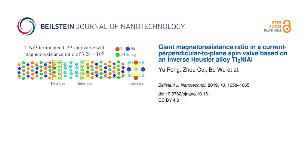
Our investigated device is a two-probe device, where Ti2NiAl is employed as a semi-infinite left and right electrode, and Ag is selected to be the middle spacer layer. For bulk Ti2NiAl, one Ti atom locates at the (0, 0, 0) site, which is described as TiA, and the other locates at the (0.25, 0.25, 0.25) site, which is described as TiB, where Ni and Al sit at (0.5, 0.5, 0.5) and (0.75, 0.75, 0.75) sites. When Ti2NiAl is applied to the device, there are two ideal terminations along the (1 0 0) direction: TiNi and TiAl. The TiNi-terminated interface can be further categorized into two patterns: (i) a TiNiT-terminated interface where interfacial Ti and Ni atoms sit on the top of Ag atoms (see Figure 1a), and (ii) a TiNiB-terminated interface where interfacial Ti and Ni atoms locate in the bridge sites between Ag atoms (see Figure 1c). In a similar manner, the TiAl-terminated interface can be further categorized into TiAlT (see Figure 1b) and TiAlB (see Figure 1d) terminated interfaces.
![[2190-4286-10-161-1]](/bjnano/content/figures/2190-4286-10-161-1.jpg?scale=2.0&max-width=1024&background=FFFFFF)
Figure 1: Schematic illustration of a Ti2NiAl/Ag/Ti2NiAl device with different atomic terminated interfaces. (a) TiNiT-terminated interface, (b)TiAlT-terminated interface, (c) TiNiB-terminated interface and (d) TiAlB-terminated interface.
Figure 1: Schematic illustration of a Ti2NiAl/Ag/Ti2NiAl device with different atomic terminated interfaces. ...
In order to study the magnetic behavior of Ti2NiAl/Ag/Ti2NiAl CPP-SV, we calculated the spin-resolved atom magnetic moment of each layer of the device with various atomic-terminated interfaces, which are shown in Figure 2. It can be seen that the magnetic moment of interfacial Tib atoms in the TiAlT-terminated (see Figure 2a) and the TiAlB-terminated structure (see Figure 2b) suffer from reduction compared to its value in bulk Ti2NiAl. Besides, magnetic moments of interfacial Tia and interfacial Ni atoms in TiNiT terminated structures (see Figure 2c) also decrease, and they become lower in TiNiB-terminated structures (see Figure 2d). This reveals that, for an interface containing Ti and Ni atoms, the hybridization between interfacial Ti and Ni atoms in the TiNiB-terminated structure is stronger than those in the TiNiT-terminated structure. The total interfacial magnetic moments of TiAlT and TiAlB terminated structures are 0.831μB and 0.871μB, respectively. The TiNiT-terminated structure has the highest total interfacial magnetic moment of 1.06μB, while the TiNiB-terminated structure owns the lowest total interfacial magnetic moment of 0.81μB. In addition, when Tia, Tib and Ni are in the deep layer of the heterostructure, their magnetic moments are close to the values in Ti2NiAl bulk, indicating that interfacial effects have a minor influence on the magnetic moment of deep-layer atoms. The magnetic property of Al atoms can be explained by the Ruderman–Kittel–Kasuya–Yosida (RKKY) indirect exchange mechanism. According to the RKKY mechanism, the magnetic coupling among d-electron atoms is transferred through the conduction electrons, and the cooperative magnetic states would exhibit ferromagnetic or antiferromagnetic alignment of the moments largely dependent upon the interatomic distances. Because the Al atom is a typical conduction sp-electron atom, it can continually exchange with local d-electrons of the nearest transition metal and serves as a bridge in hybridization between local d-electrons atoms. Hence, the atomic magnetic moment of the Al atom always presents a small negative value.
![[2190-4286-10-161-2]](/bjnano/content/figures/2190-4286-10-161-2.png?scale=2.0&max-width=1024&background=FFFFFF)
Figure 2: The calculated atomic spin magnetic moment of Ti2NiAl/Ag/Ti2NiAl CPP-SV at different atomic layers. (a) TiAlT-terminated structure, (b) TiAlB-terminated structure, (c) TiNiT-terminated structure and (d) TiNiB-terminated structure.
Figure 2: The calculated atomic spin magnetic moment of Ti2NiAl/Ag/Ti2NiAl CPP-SV at different atomic layers....
Because the interface spin polarization (ISP) plays an important role in determining the performance of a spin-dependent device, the interfacial electronic structure is calculated and exhibited in Figure 3, where the left panel and right panel indicate the interfacial electronic structure in spin up and spin down channels, respectively. It was observed that the spin down half-metallic energy gap in bulk Ti2NiAl is destroyed completely in various kinds of atomic-terminated interfaces of the Ti2NiAl/Ag/Ti2NiAl device, which could be attributed to the appearance of interface states [27,28]. As for interfaces containing Ti and Ni atoms, spin up and spin down density of states at the Fermi level in the TiNiT-terminated structure are close to those in the TiNiB-terminated structure, and the spin up density of states at the Fermi level are higher than spin down density of states at the Fermi level. As for interfaces containing Ti and Al atoms, spin up and spin down density of states at the Fermi level in both TiAlT and TiAlB terminated structures are much lower than in TiNiT and TiNiB terminated structures, and the spin up density of states at the Fermi level are comparable to spin down density of states at the Fermi level. The ISP can be defined as ISP = (N↑ − N↓)/(N↑ + N↓), where N↑ and N↓ represent the spin up and spin down contributions to the total density of states (DOS) at the Fermi level, respectively. Table 1 shows that the calculated ISP of the TiAlB-terminated structure is ≈30%, and it decreases to ≈20% in the TiAlT-terminated structure, which is the lowest ISP value. However, the TiNiT-terminated structure has a high ISP of ≈42%, and the TiNiB-terminated structure possesses the largest ISP of ≈55%.
![[2190-4286-10-161-3]](/bjnano/content/figures/2190-4286-10-161-3.png?scale=2.0&max-width=1024&background=FFFFFF)
Figure 3: Density of states of the interface of the Ti2NiAl/Ag/Ti2NiAl device with different atomic terminated interface.
Figure 3: Density of states of the interface of the Ti2NiAl/Ag/Ti2NiAl device with different atomic terminate...
Table 1: The calculated interface spin polarization (ISP), transmission coefficients at the Fermi level, and magnetoresistance ratio (MR) of the Ti2NiAl/Ag/Ti2NiAl device with various atomic terminations.
| Termination | ISP |
![[Graphic 1]](/bjnano/content/inline/2190-4286-10-161-i2.svg?max-width=637&scale=1.18182)
|
![[Graphic 2]](/bjnano/content/inline/2190-4286-10-161-i3.svg?max-width=637&scale=1.18182)
|
![[Graphic 3]](/bjnano/content/inline/2190-4286-10-161-i4.svg?max-width=637&scale=1.18182)
|
![[Graphic 4]](/bjnano/content/inline/2190-4286-10-161-i5.svg?max-width=637&scale=1.18182)
|
MR |
|---|---|---|---|---|---|---|
| TiNiT | ≈42% | 0.1067 | 0 | 0.1657 × 10⁻⁶ | 0.1869 × 10⁻⁶ | 3.03 × 10⁵ |
| TiNiB | ≈55% | 0.1152 | 0 | 0.2041 × 10⁻⁶ | 0.1472 × 10⁻⁶ | 3.28 × 10⁵ |
| TiAlT | ≈20% | 0.0408 | 0 | 0.2243 × 10⁻⁶ | 0.1991 × 10⁻⁶ | 9.64 × 10⁴ |
| TiAlB | ≈30% | 0.0991 | 0 | 0.7354 × 10⁻⁶ | 0.7486 × 10⁻⁶ | 6.67 × 10⁴ |
As for our two-probe device, the spin-dependent transmission coefficient Tσ(E) can be calculated employing Tσ(E) = Tr[ГLGRГRGA], where ГL and ГR are the coupling matrix of the left and right electrode, respectively; GR and GA are the retarded and advanced Green’s function of the central region, respectively; and σ is the spin direction, spin up or spin down. A two magnetization configuration is considered, thus the two electrodes of the device are in parallel magnetization configuration (PC) and in antiparallel magnetization configuration (APC). The spin-dependent electron transmission curves of spin up and spin down channels of the device with different atomic terminated interfaces in PC and APC are calculated and shown in Figure 4, where the green dashed line indicates the Fermi level, which is set to zero. It can be seen that in APC, for all four kinds of interface structures, both the spin up and spin down channels, possess a very small transport coefficient at the Fermi level. This indicates that the spin up and spin down channels are blocked when the device is in the APC state, i.e., the spin-polarized current cannot be detected, and the device is turned off. When the device is in the PC state, a spin up transmission coefficient at the Fermi level (![[Graphic 5]](/bjnano/content/inline/2190-4286-10-161-i6.svg?max-width=637&scale=1.18182) ) is much higher than the spin down transmission coefficient at the Fermi level (
) is much higher than the spin down transmission coefficient at the Fermi level (![[Graphic 6]](/bjnano/content/inline/2190-4286-10-161-i7.svg?max-width=637&scale=1.18182) ). This reveals that when the device is in the PC state, the spin up channel is unlocked and spin up electrons, which are regarded as the majority of spin electrons, can flow from the left electrode to the right electrode through a Ag spacer. In contrast, the spin down channel is still closed, and the spin down electrons, which are regarded as the minority of spin electrons, are suppressed. Hence, spin-polarized current can be detected when the device is in the PC state, and it is mainly dominated by spin up electrons, and the device is in a “turn on” mode. As for the device with an interface containing Ti and Ni atoms, in the PC state, the value of
). This reveals that when the device is in the PC state, the spin up channel is unlocked and spin up electrons, which are regarded as the majority of spin electrons, can flow from the left electrode to the right electrode through a Ag spacer. In contrast, the spin down channel is still closed, and the spin down electrons, which are regarded as the minority of spin electrons, are suppressed. Hence, spin-polarized current can be detected when the device is in the PC state, and it is mainly dominated by spin up electrons, and the device is in a “turn on” mode. As for the device with an interface containing Ti and Ni atoms, in the PC state, the value of ![[Graphic 7]](/bjnano/content/inline/2190-4286-10-161-i8.svg?max-width=637&scale=1.18182) in the TiNiT-terminated structure (0.1067) is comparable to the value in the TiNiB-terminated structure (0.1152). In the APC state, the values of
in the TiNiT-terminated structure (0.1067) is comparable to the value in the TiNiB-terminated structure (0.1152). In the APC state, the values of ![[Graphic 8]](/bjnano/content/inline/2190-4286-10-161-i9.svg?max-width=637&scale=1.18182) and
and ![[Graphic 9]](/bjnano/content/inline/2190-4286-10-161-i10.svg?max-width=637&scale=1.18182) in the TiNiT-terminated structure are also close to the values in the TiNiB-terminated structure. Besides, as for the device with an interface containing Ti and Al atoms, the value of
in the TiNiT-terminated structure are also close to the values in the TiNiB-terminated structure. Besides, as for the device with an interface containing Ti and Al atoms, the value of ![[Graphic 10]](/bjnano/content/inline/2190-4286-10-161-i11.svg?max-width=637&scale=1.18182) in the TiAlT-terminated structure is 0.0408, and it increases to 0.099 in the TiAlB-terminated structure. Nevertheless, it can be found that the device with the TiNi-terminated interface possesses a higher spin up transmission coefficient than the TiAl-terminated interface.
in the TiAlT-terminated structure is 0.0408, and it increases to 0.099 in the TiAlB-terminated structure. Nevertheless, it can be found that the device with the TiNi-terminated interface possesses a higher spin up transmission coefficient than the TiAl-terminated interface.
![[2190-4286-10-161-4]](/bjnano/content/figures/2190-4286-10-161-4.png?scale=2.0&max-width=1024&background=FFFFFF)
Figure 4: Transmission coefficient versus electron energy in the parallel magnetization configuration (PC) and antiparallel magnetization configuration (APC) of the Ti2NiAl/Ag/Ti2NiAl device with different atomic terminated interfaces. The dashed line is the Fermi level. (a) TiNiT-terminated structure, (b) TiAlT-terminated structure, (c) TiNiB-terminated structure and (d) TiAlB-terminated structure.
Figure 4: Transmission coefficient versus electron energy in the parallel magnetization configuration (PC) an...
In order to further exhibit the spin-transport behavior of the device, the transmission coefficient at the Fermi level of various kinds of structures in the two-dimensional Brillouin zone, which is perpendicular to the spin-transport direction, was calculated. In Figure 5, the contour plots of the transmission coefficient at the Fermi level are shown as a function of kx and ky and indicate the transport behavior of spin up electrons of the device in the PC state. The plots in the middle column and the right column indicate the transport behavior of spin up and spin down electrons, respectively, of the device in the APC state. There are two color bars in Figure 5, and the upper color bar and the lower color bar represent the amplitude of the transport ability at various (kx, ky) points when the device is in the PC and APC state, respectively. It was observed that when the device has different atomic terminated interfaces in the PC state, the magnitude of the hot spots in the spin up channel is much stronger than those in the spin up and spin down channels of the device in APC. This reveals that when the device is in the APC state, the transport ability of spin up and spin down electrons is inhibited, and spin-polarized electrons are less likely to travel from the left electrode to the right electrode. Besides, in the PC state the magnitude of the spin up channel of the TiNiT-terminated structure is comparable to that of the TiNiB and TiAlB structures, while it becomes weaker in the TiAlT termination. This reveals that when the device in the PC state, the spin up electrons of the TiNiT, TiNiB and TiAlB terminated structures have a similar intensity of transport ability, while the transport ability of the spin up electrons of the TiAlT terminated structure suffers from deterioration. Now, the situation when the device is in the APC state will be discussed. It can be seen that in the APC state, the transmission spectra of the spin up channel are nearly the same as that of the spin down channel for all kinds of atomic terminated structures, revealing that the transport ability of the spin up electrons is close to that of the spin down electrons. This results in the consequence that when the device is in the APC state, it is difficult to identify the spin up current and the spin down current from the total spin-polarized current.
![[2190-4286-10-161-5]](/bjnano/content/figures/2190-4286-10-161-5.jpg?scale=2.0&max-width=1024&background=FFFFFF)
Figure 5: The k//-resolved transmission coefficients at the Fermi level of the Ti2NiAl/Ag/Ti2NiAl CPP-SV with different atomic terminated interfaces.
Figure 5: The k//-resolved transmission coefficients at the Fermi level of the Ti2NiAl/Ag/Ti2NiAl CPP-SV with...
As one the most significant parameters in spintronics devices, the magnetoresistance (MR) ratio (when the device at equilibrium) can be calculated by
![[2190-4286-10-161-i1]](/bjnano/content/inline/2190-4286-10-161-i1.svg?max-width=590&scale=1.18182)
where TPC(Ef) and TAPC(Ef) indicate the total transmission coefficient at the Fermi level in the PC and APC states, where
![[Graphic 11]](/bjnano/content/inline/2190-4286-10-161-i12.svg?max-width=637&scale=1.18182)
The MR ratios of the Ti2NiAl/Ag/Ti2NiAl device with various kinds of atomic terminated interfaces were calculated and listed in Table 1. It can be seen that the MR ratios of all the structures exceed ≈104 order of magnitude. The device with a TiAlB interface shows a high MR ratio of 6.67 × 10⁴, and the MR ratio is boosted to a higher value of 9.64 × 10⁴ for the TiAlT interface structure. This reveals that for the Ti2NiAl/Ag/Ti2NiAl device with an interface containing Ti and Al atoms, the Heusler layer sits on the top site of the Ag atom and can produce larger a MR ratio than when it sits at the bridge site of the Ag atom. On the other hand, the MR ratio of the device with the TiNiT terminated interface reaches up to 3.03 × 10⁵, and the MR ratio is further enhanced to an ultrahigh value of 3.28 × 10⁵ in the device with the TiNiB terminated interface. Therefore, it can be deduced that the Ti2NiAl/Ag/Ti2NiAl device with the interface containing Ti and Ni atoms generally results in a higher MR ratio than that with interfaces containing Ti and Al atoms. Additionally, the device with a TiNiB-terminated interface possesses the largest MR value and can be regarded as a promising candidate for furture spintronics devices.
Conclusion
By employing first principles calculations combined with the nonequilibrium Green’s function, we studied the interfacial magnetic properties, interfacial electronic structure and spin transport properties of a Ti2NiAl/Al/Ti2NiAl CPP-SV and four structures with different atomic terminated interfaces were modeled. Our calculation revealed that the magnetic moments of atoms located at the interface suffer a decrease, while the magnetic moments of atoms that sit at deep layers are close to corresponding values in bulk Ti2NiAl. The TiNiT-terminated structure possesses a high ISP of ≈42%, and the TiNiB-terminated structure has the largest ISP of ≈55%. The total transmission coefficient at the Fermi level mainly comes from the contribution of the spin up electrons, which is regarded as the majority of spin electrons. In the PC state, the spin up transmission coefficients of TiNiT and TiNiB terminated structures are higher than that of TiAlT and TiAlB terminated structures. The MR ratios of the device with four different interfaces, i.e., TiAlT, TiAlB, TiNiT and TiNiB terminated interfaces, have been calculated. Our calculation reveals that the device with TiNiB-terminated structure possesses the largest MR ratio of 3.28 × 10⁵, a value that is much higher than other CPP-SV devices such as Fe4N/Ag/Fe4N and Co2MnAl/Ag/Co2MnAl. Such a high MR ratio could be attributed to the complete spin-polarized Ti2NiAl bulk and high spin polarization at the interface of the device. Therefore, Ti2NiAl/Ag/Ti2NiAl CPP-SV has great application potential in spintronic devices.
Simulation Details
The Ti2NiAl/Ag/Ti2NiAl device with four different atomic terminated interfaces was geometrically optimized by utilizing a density functional theory (DFT)-based Vienna ab-initio simulation package (VASP) [31,32]. Ti (3d24s2), Ni (3d84s2), Al (3s23p1) and Ag (4d105s1) were chosen to be the valence electron configurations. The exchange-correlation interaction is described by the Perdew–Burke–Ernzerhof (PBE) generalized gradient approximation (GGA). A Monkhorst–Pack grid of 13 × 13 × 1 for k-point sampling, a self-consistent field (SCF) convergence criterion of 1 × 10⁻⁵ eV, and a plane-wave basis cutoff energy of 550 eV were applied. The Keldysh nonequilibrium Green’s function (NEGF) theory, as implemented in Nanodcal package [33,34], was employed to investigate the spin-transport properties of the Ti2NiAl/Ag/Ti2NiAl device. In our calculations of transport properties, the number of Monkhorst–Pack k-space grids of the left and right electrode is 10 × 10 × 100, and that of the central scattering region is 10 × 10 × 1, where the self-consistent calculations are limited to 10−5 Hartree tolerance.
References
-
de Groot, R. A.; Mueller, F. M.; Engen, P. G. v.; Buschow, K. H. J. Phys. Rev. Lett. 1983, 50, 2024–2027. doi:10.1103/physrevlett.50.2024
Return to citation in text: [1] -
Hirohata, A.; Takanashi, K. J. Phys. D: Appl. Phys. 2014, 47, 193001. doi:10.1088/0022-3727/47/19/193001
Return to citation in text: [1] -
Li, X.; Yang, J. Natl. Sci. Rev. 2016, 3, 365–381. doi:10.1093/nsr/nww026
Return to citation in text: [1] -
Nakatani, T. M.; Furubayashi, T.; Kasai, S.; Sukegawa, H.; Takahashi, Y. K.; Mitani, S.; Hono, K. Appl. Phys. Lett. 2010, 96, 212501. doi:10.1063/1.3432070
Return to citation in text: [1] -
Valet, T.; Fert, A. Phys. Rev. B 1993, 48, 7099–7113. doi:10.1103/physrevb.48.7099
Return to citation in text: [1] -
Kamashev, A. A.; Validov, A. A.; Schumann, J.; Kataev, V.; Büchner, B.; Fominov, Y. V.; Garifullin, I. A. Beilstein J. Nanotechnol. 2018, 9, 1764–1769. doi:10.3762/bjnano.9.167
Return to citation in text: [1] -
Takahashi, Y. K.; Hase, N.; Kodzuka, M.; Itoh, A.; Koganezawa, T.; Furubayashi, T.; Li, S.; Varaprasad, B. S. D. C. S.; Ohkubo, T.; Hono, K. J. Appl. Phys. 2013, 113, 223901. doi:10.1063/1.4809643
Return to citation in text: [1] -
Hase, N.; Varaprasad, B. S. D. C. S.; Nakatani, T. M.; Sukegawa, H.; Kasai, S.; Takahashi, Y. K.; Furubayashi, T.; Hono, K. J. Appl. Phys. 2010, 108, 093916. doi:10.1063/1.3503869
Return to citation in text: [1] -
Takahashi, Y. K.; Srinivasan, A.; Varaprasad, B.; Rajanikanth, A.; Hase, N.; Nakatani, T. M.; Kasai, S.; Furubayashi, T.; Hono, K. Appl. Phys. Lett. 2011, 98, 152501. doi:10.1063/1.3576923
Return to citation in text: [1] -
Sakuraba, Y.; Ueda, M.; Miura, Y.; Sato, K.; Bosu, S.; Saito, K.; Shirai, M.; Konno, T. J.; Takanashi, K. Appl. Phys. Lett. 2012, 101, 252408. doi:10.1063/1.4772546
Return to citation in text: [1] -
Sakuraba, Y.; Izumi, K.; Iwase, T.; Bosu, S.; Saito, K.; Takanashi, K.; Miura, Y.; Futatsukawa, K.; Abe, K.; Shirai, M. Phys. Rev. B 2010, 82, 094444. doi:10.1103/physrevb.82.094444
Return to citation in text: [1] -
Feng, Y.; Cui, Z.; Wei, M.-s.; Wu, B. Appl. Surf. Sci. 2019, 466, 78–83. doi:10.1016/j.apsusc.2018.09.247
Return to citation in text: [1] -
Han, J.; Feng, Y.; Yao, K.; Gao, G. Y. Appl. Phys. Lett. 2017, 111, 132402. doi:10.1063/1.4999288
Return to citation in text: [1] -
Zhang, X.; Tao, L. L.; Zhang, J.; Liang, S. H.; Jiang, L.; Han, X. F. Appl. Phys. Lett. 2017, 110, 252403. doi:10.1063/1.4986449
Return to citation in text: [1] -
Han, J.; Gao, G. Appl. Phys. Lett. 2018, 113, 102402. doi:10.1063/1.5047151
Return to citation in text: [1] -
Skaftouros, S.; Özdoğan, K.; Şaşıoğlu, E.; Galanakis, I. Phys. Rev. B 2013, 87, 024420. doi:10.1103/physrevb.87.024420
Return to citation in text: [1] -
Gilleßen, M.; Dronskowski, R. J. Comput. Chem. 2010, 31, 612. doi:10.1002/jcc.21358
Return to citation in text: [1] -
Ma, J. H.; He, J. G.; Dipanjan, M.; Kamaram, M.; Sahar, K.; Tim, L.; Wolverton, C.; Ghosh, A. W.; Butler, W. H. Phys. Rev. B 2018, 98, 094410. doi:10.1103/physrevb.98.094410
Return to citation in text: [1] -
Ahmadian, F.; Salary, A. Intermetallics 2014, 46, 243–249. doi:10.1016/j.intermet.2013.11.021
Return to citation in text: [1] -
Taşkın, F.; Atiş, M.; Canko, O.; Kervan, S.; Kervan, N. J. Magn. Magn. Mater. 2017, 426, 473. doi:10.1016/j.jmmm.2016.06.071
Return to citation in text: [1] -
Lei, F.; Tang, C.; Wang, S.; He, W. J. Alloys Compd. 2011, 509, 5187–5189. doi:10.1016/j.jallcom.2011.02.002
Return to citation in text: [1] -
Jakobsson, A.; Mavropoulos, P.; Şaşıoğlu, E.; Blügel, S.; Ležaić, M.; Sanyal, B.; Galanakis, I. Phys. Rev. B 2015, 91, 174439. doi:10.1103/physrevb.91.174439
Return to citation in text: [1] -
Ouardi, S.; Fecher, G. H.; Felser, C.; Kübler, J. Phys. Rev. Lett. 2013, 110, 100401. doi:10.1103/physrevlett.110.100401
Return to citation in text: [1] -
Jamer, M. E.; Assaf, B. A.; Devakul, T.; Heiman, D. Appl. Phys. Lett. 2013, 103, 142403. doi:10.1063/1.4823601
Return to citation in text: [1] -
Xu, G. Z.; Du, Y.; Zhang, X. M.; Zhang, H. G.; Liu, E. K.; Wang, W. H.; Wu, G. H. Appl. Phys. Lett. 2014, 104, 242408. doi:10.1063/1.4884203
Return to citation in text: [1] -
Lukashev, P.; Kharel, P.; Gilbert, S.; Staten, B.; Hurley, N.; Fuglsby, R.; Huh, Y.; Valloppilly, S.; Zhang, W.; Yang, K.; Skomski, R.; Sellmyer, D. J. Appl. Phys. Lett. 2016, 108, 141901. doi:10.1063/1.4945600
Return to citation in text: [1] -
Shi, W.; Muechler, L.; Manna, K.; Zhang, Y.; Koepernik, K.; Car, R.; van den Brink, J.; Felser, C.; Sun, Y. Phys. Rev. B 2018, 97, 060406. doi:10.1103/physrevb.97.060406
Return to citation in text: [1] [2] -
Li, J.; Jin, Y. Appl. Surf. Sci. 2013, 283, 876–880. doi:10.1016/j.apsusc.2013.07.036
Return to citation in text: [1] [2] -
Feng, Y.; Zhou, T.; Chen, X.; Yuan, H.; Chen, H. J. Phys. D: Appl. Phys. 2015, 48, 285302. doi:10.1088/0022-3727/48/28/285302
Return to citation in text: [1] -
Feng, Y.; Wu, B.; Yuan, H.; Kuang, A.; Chen, H. J. Alloys Compd. 2013, 557, 202–208. doi:10.1016/j.jallcom.2012.12.134
Return to citation in text: [1] -
Hohenberg, P.; Kohn, W. Phys. Rev. 1964, 136, B864–B871. doi:10.1103/physrev.136.b864
Return to citation in text: [1] -
Kohn, W.; Sham, L. J. Phys. Rev. 1965, 140, A1133–A1138. doi:10.1103/physrev.140.a1133
Return to citation in text: [1] -
Taylor, J.; Guo, H.; Wang, J. Phys. Rev. B 2001, 63, 245407. doi:10.1103/physrevb.63.245407
Return to citation in text: [1] -
Waldron, D.; Haney, P.; Larade, B.; MacDonald, A.; Guo, H. Phys. Rev. Lett. 2006, 96, 166804. doi:10.1103/physrevlett.96.166804
Return to citation in text: [1]
| 26. | Lukashev, P.; Kharel, P.; Gilbert, S.; Staten, B.; Hurley, N.; Fuglsby, R.; Huh, Y.; Valloppilly, S.; Zhang, W.; Yang, K.; Skomski, R.; Sellmyer, D. J. Appl. Phys. Lett. 2016, 108, 141901. doi:10.1063/1.4945600 |
| 27. | Shi, W.; Muechler, L.; Manna, K.; Zhang, Y.; Koepernik, K.; Car, R.; van den Brink, J.; Felser, C.; Sun, Y. Phys. Rev. B 2018, 97, 060406. doi:10.1103/physrevb.97.060406 |
| 21. | Lei, F.; Tang, C.; Wang, S.; He, W. J. Alloys Compd. 2011, 509, 5187–5189. doi:10.1016/j.jallcom.2011.02.002 |
| 22. | Jakobsson, A.; Mavropoulos, P.; Şaşıoğlu, E.; Blügel, S.; Ležaić, M.; Sanyal, B.; Galanakis, I. Phys. Rev. B 2015, 91, 174439. doi:10.1103/physrevb.91.174439 |
| 23. | Ouardi, S.; Fecher, G. H.; Felser, C.; Kübler, J. Phys. Rev. Lett. 2013, 110, 100401. doi:10.1103/physrevlett.110.100401 |
| 24. | Jamer, M. E.; Assaf, B. A.; Devakul, T.; Heiman, D. Appl. Phys. Lett. 2013, 103, 142403. doi:10.1063/1.4823601 |
| 25. | Xu, G. Z.; Du, Y.; Zhang, X. M.; Zhang, H. G.; Liu, E. K.; Wang, W. H.; Wu, G. H. Appl. Phys. Lett. 2014, 104, 242408. doi:10.1063/1.4884203 |
| 1. | de Groot, R. A.; Mueller, F. M.; Engen, P. G. v.; Buschow, K. H. J. Phys. Rev. Lett. 1983, 50, 2024–2027. doi:10.1103/physrevlett.50.2024 |
| 7. | Takahashi, Y. K.; Hase, N.; Kodzuka, M.; Itoh, A.; Koganezawa, T.; Furubayashi, T.; Li, S.; Varaprasad, B. S. D. C. S.; Ohkubo, T.; Hono, K. J. Appl. Phys. 2013, 113, 223901. doi:10.1063/1.4809643 |
| 19. | Ahmadian, F.; Salary, A. Intermetallics 2014, 46, 243–249. doi:10.1016/j.intermet.2013.11.021 |
| 6. | Kamashev, A. A.; Validov, A. A.; Schumann, J.; Kataev, V.; Büchner, B.; Fominov, Y. V.; Garifullin, I. A. Beilstein J. Nanotechnol. 2018, 9, 1764–1769. doi:10.3762/bjnano.9.167 |
| 20. | Taşkın, F.; Atiş, M.; Canko, O.; Kervan, S.; Kervan, N. J. Magn. Magn. Mater. 2017, 426, 473. doi:10.1016/j.jmmm.2016.06.071 |
| 5. | Valet, T.; Fert, A. Phys. Rev. B 1993, 48, 7099–7113. doi:10.1103/physrevb.48.7099 |
| 2. | Hirohata, A.; Takanashi, K. J. Phys. D: Appl. Phys. 2014, 47, 193001. doi:10.1088/0022-3727/47/19/193001 |
| 3. | Li, X.; Yang, J. Natl. Sci. Rev. 2016, 3, 365–381. doi:10.1093/nsr/nww026 |
| 4. | Nakatani, T. M.; Furubayashi, T.; Kasai, S.; Sukegawa, H.; Takahashi, Y. K.; Mitani, S.; Hono, K. Appl. Phys. Lett. 2010, 96, 212501. doi:10.1063/1.3432070 |
| 16. | Skaftouros, S.; Özdoğan, K.; Şaşıoğlu, E.; Galanakis, I. Phys. Rev. B 2013, 87, 024420. doi:10.1103/physrevb.87.024420 |
| 17. | Gilleßen, M.; Dronskowski, R. J. Comput. Chem. 2010, 31, 612. doi:10.1002/jcc.21358 |
| 18. | Ma, J. H.; He, J. G.; Dipanjan, M.; Kamaram, M.; Sahar, K.; Tim, L.; Wolverton, C.; Ghosh, A. W.; Butler, W. H. Phys. Rev. B 2018, 98, 094410. doi:10.1103/physrevb.98.094410 |
| 11. | Sakuraba, Y.; Izumi, K.; Iwase, T.; Bosu, S.; Saito, K.; Takanashi, K.; Miura, Y.; Futatsukawa, K.; Abe, K.; Shirai, M. Phys. Rev. B 2010, 82, 094444. doi:10.1103/physrevb.82.094444 |
| 13. | Han, J.; Feng, Y.; Yao, K.; Gao, G. Y. Appl. Phys. Lett. 2017, 111, 132402. doi:10.1063/1.4999288 |
| 31. | Hohenberg, P.; Kohn, W. Phys. Rev. 1964, 136, B864–B871. doi:10.1103/physrev.136.b864 |
| 32. | Kohn, W.; Sham, L. J. Phys. Rev. 1965, 140, A1133–A1138. doi:10.1103/physrev.140.a1133 |
| 10. | Sakuraba, Y.; Ueda, M.; Miura, Y.; Sato, K.; Bosu, S.; Saito, K.; Shirai, M.; Konno, T. J.; Takanashi, K. Appl. Phys. Lett. 2012, 101, 252408. doi:10.1063/1.4772546 |
| 14. | Zhang, X.; Tao, L. L.; Zhang, J.; Liang, S. H.; Jiang, L.; Han, X. F. Appl. Phys. Lett. 2017, 110, 252403. doi:10.1063/1.4986449 |
| 33. | Taylor, J.; Guo, H.; Wang, J. Phys. Rev. B 2001, 63, 245407. doi:10.1103/physrevb.63.245407 |
| 34. | Waldron, D.; Haney, P.; Larade, B.; MacDonald, A.; Guo, H. Phys. Rev. Lett. 2006, 96, 166804. doi:10.1103/physrevlett.96.166804 |
| 9. | Takahashi, Y. K.; Srinivasan, A.; Varaprasad, B.; Rajanikanth, A.; Hase, N.; Nakatani, T. M.; Kasai, S.; Furubayashi, T.; Hono, K. Appl. Phys. Lett. 2011, 98, 152501. doi:10.1063/1.3576923 |
| 28. | Li, J.; Jin, Y. Appl. Surf. Sci. 2013, 283, 876–880. doi:10.1016/j.apsusc.2013.07.036 |
| 29. | Feng, Y.; Zhou, T.; Chen, X.; Yuan, H.; Chen, H. J. Phys. D: Appl. Phys. 2015, 48, 285302. doi:10.1088/0022-3727/48/28/285302 |
| 30. | Feng, Y.; Wu, B.; Yuan, H.; Kuang, A.; Chen, H. J. Alloys Compd. 2013, 557, 202–208. doi:10.1016/j.jallcom.2012.12.134 |
| 8. | Hase, N.; Varaprasad, B. S. D. C. S.; Nakatani, T. M.; Sukegawa, H.; Kasai, S.; Takahashi, Y. K.; Furubayashi, T.; Hono, K. J. Appl. Phys. 2010, 108, 093916. doi:10.1063/1.3503869 |
| 12. | Feng, Y.; Cui, Z.; Wei, M.-s.; Wu, B. Appl. Surf. Sci. 2019, 466, 78–83. doi:10.1016/j.apsusc.2018.09.247 |
| 27. | Shi, W.; Muechler, L.; Manna, K.; Zhang, Y.; Koepernik, K.; Car, R.; van den Brink, J.; Felser, C.; Sun, Y. Phys. Rev. B 2018, 97, 060406. doi:10.1103/physrevb.97.060406 |
| 28. | Li, J.; Jin, Y. Appl. Surf. Sci. 2013, 283, 876–880. doi:10.1016/j.apsusc.2013.07.036 |
© 2019 Feng et al.; licensee Beilstein-Institut.
This is an Open Access article under the terms of the Creative Commons Attribution License (http://creativecommons.org/licenses/by/4.0). Please note that the reuse, redistribution and reproduction in particular requires that the authors and source are credited.
The license is subject to the Beilstein Journal of Nanotechnology terms and conditions: (https://www.beilstein-journals.org/bjnano)