Abstract
Based on an electrochemical method, three-dimensional arrayed nanopore structures are machined onto a Mg surface. The structured Mg surface is coated with a thin gold (Au) film, which is used as a surface-enhanced Raman scattering (SERS) substrate. A rhodamine 6G (R6G) probe molecule is used as the detection agent for the SERS measurement. Different sizes of arrayed micro/nanostructures are fabricated by different treatment time using the electrochemical process. The topographies of these micro/nanostructures and the thickness of the Au film have an influence on the Raman intensity of the Mg substrate. Furthermore, when the thickness of Au film coating is held constant, the Raman intensity on the structured Mg substrates is about five times higher after a treatment time of 1 min when compared with other treatment times. The SERS enhancement factor ranges from 106 to 1.75 × 10⁷ under these experimental conditions. Additionally, a 10−6 mol·L−1 solution of lysozyme was successfully detected using the Mg–Au nanopore substrates. Our low-cost method is reproducible, homogeneous, and suitable for the fabrication of SERS substrates.
Introduction
Surface-enhanced Raman spectroscopy (SERS) can be used to detect biomolecules [1-3], explosives [4-6], and pesticide residues [7-9]. Plasmonic metal nanostructures are often used as SERS substrates to increase the molecule-specific Raman signal by several orders of magnitude. The functionality of SERS is due to a combination of surface electron movement in the substrate and charge transfer between substrate and the analyte molecules, in contrast to the typical signal intensity elicited during spontaneous Raman spectroscopy, which is extremely weak [10,11]. SERS is representative of other technologies that can amplify signal intensities based on strong electromagnetic fields and chemical enhancement [12-14].
Recently, all kinds of shapes of nanostructures machined by several researchers as SERS substrates have been machined by using lithography-based method [15-20]. Additionally, nanostructures are also fabricated by hybrid lithography [21-26] methods combined with dry etching or wet etching. For example, the commercial Klarite substrate [21-23] machined by electron beam lithography (EBL) and wet etching consists of 1 μm deep square-based pyramidal pits in the silicon surface. A rhodamine solution (10−4 mol·L−1) is then detected using the Klarite substrate. Candeloro et al. [24] employed EBL and reactive ion etching to machine nanoholes of 400 nm diameter and 50 nm depth. Subsequently, nanoholes were transferred onto the glass surface using the peeling template method and R6G molecules (10−6 mol·L−1) were used with the substrate for detection. Au nanostructures of different shapes and sizes (including grating, disk, and pyramid structures) have also been fabricated using EBL and reactive ion etching methods [25]. The Raman intensities of R6G and 4-mercaptopyridine molecules were measured by using different substrates. In addition, the Raman intensity of R6G on the pyramid structures was higher than that of R6G on the other structures in the experiment, and the enhancement factor of R6G molecules on the pyramid structure was about 105. Wu et al. [26] machined nanohole array structures using EBL and lift-off methods. The diameter of the nanoholes ranged from 90 to 585 nm, and the gap between adjacent nanoholes ranged from 125 to 585 nm. An enhancement factor of 8 × 10⁶ was achieved for 4-mercaptobenzoic acid molecules on the arrayed Au nanoholes. However, lithography-based methods have limitations, as they are inefficient and cannot be exploited for mass production. In addition, it is challenging to use the existing methods to fabricate more complex nanostructures.
Focused ion beam (FIB) technology can also be used to directly fabricate high-precision nanostructures on surfaces made of silicon, silicon dioxide and metal [27-33]. FIB technology is therefore used as a processing method for SERS substrates. Using the FIB method, Lin et al. [29] fabricated micro/nanostructures on the surface of Au-coated single crystal silicon. By changing the etching time and current, micro/nanostructures with different size scales and geometric shapes (such as hexagons and pentagons) were obtained. Compared with other geometries, the hexagonal micro/nanostructure surface yielded the highest Raman intensity during the detection of R6G molecules. In addition, the spatial distance of the micro/nanostructures ranges from 22 to 83 nm, and the Raman intensity of R6G increases exponentially as the distance between adjacent micro/nanostructures decreases. Gao et al. [30] fabricated elliptical nanostructures and studied the effect of processing distance parameters and gold film thickness on the Raman intensity of R6G. They found that the Raman intensity of R6G was highest on densely packed structures. Additionally, the Raman intensity of R6G decreases as the number of hot spots decreases. Sivashanmugan et al. [32] employed FIB technology to prepare nanostructures on silicon surfaces, which were then coated with Au and Ag films to generate SERS substrates. The enhancement factor range of R6G using the substrate was between 2.62 × 10⁶ and 1.74 × 10⁷. Gao et al. [33] machined elliptic nanostructures with different parameters on Si substrates, including the spacing between structures and the thickness of the gold film. A spacing of 15 nm between the adjacent nanostructures was for the detection of R6G molecules with a concentration of 10−6 mol·L−1. Compared with other processing methods, the precision of FIB processing technology is relatively high. However, FIB processing is an expensive and low-throughput technology. In addition, the processing time of a wide range of micro/nanostructures is long. Therefore, the low-cost and efficient preparation of array nanostructures with controllable shape, size and density is urgently required for SERS substrates for molecular recognition.
Some researchers have fabricated nanostructures as SERS substrates by using electrochemical oxidation–reduction cycle (ORC) methods [34-39]. Generally, sheets of Au and Pt, and a KCl-saturated Ag/AgCl rod are used as the working, counter, and reference electrodes, respectively. Using this approach, Au/TiO2 nanocomposites formed on Pt substrates yielded a SERS enhancement factor of 1.8 × 10⁸ for R6G molecules [34]. Chang et al. [35] fabricated different Ag nanostructures on Pt substrates using a sonoelectrochemical ORC method with different ratios between the time periods of deposition and dissolution. The detection level of R6G molecules was 2 × 10⁻¹³ mol·L−1 and the highest enhancement factor achieved was 2.3 × 10⁸. Yang et al. [36] used ORC treatments in KCl solution to fabricate roughened Ag substrates. In this system, the limit of detection for R6G with SERS was 2 × 10⁻⁸ mol·L−1. Based on a ORC method, Chen et al. [37] created hybrid Au–AuOx with reverse rates of 200, 100, 50, 25, and 5 mV/s. The highest enhancement factor observed with R6G in this system was 5.5 × 10⁶ with a reverse rate of 25 mV/s. Furthermore, pigments of Brilliant Blue FCF and Indigo Carmine at concentrations as low as 10−8 mol·L−1 and 10−7 mol·L−1, respectively, were detectable using the SERS substrate. Ou et al. [38] prepared Ag SERS substrates by using triangular-wave ORC procedures in KCl solution. In this study, the Raman intensity of R6G (2 × 10⁻⁶ mol·L−1) on the Ag substrate was larger with subsequent drying treatment than without.
Anodic aluminum oxide (AAO) has been used as a mask to fabricate nanodot SERS substrates [40-43]. Using an AAO mask, Han et al. [41] manufactured graphene/Au nanodot array structures, which were used as SERS substrates. The diameter and gap distribution ranged from 30 to 42 nm and from 20 to 30 nm, respectively. In addition, a detection level of 10−9 mol·L−1 for R6G molecules was obtained using the aforementioned SERS substrates. Choi et al. [42] used a nanoporous template of AAO as a SERS substrate, and varied the thickness of either the Au film or the AAO itself. An enhancement factor of 107 was obtained with an Au thickness of 20 nm and an AAO thickness of 100 nm. Using an AAO template, Aflatoxin B1 (AFB1) from peanut extract was detected at concentrations ranging from 1.5 µg/L to 1.5 mg/L. Although the method is suitable for the evaluation of AFB1 content in food safety inspections [43], the fabrication process for generating the AAO is lengthy.
In this paper, a simple and rapid electrochemical micromachining approach is presented for fabricating sensitive three-dimensional SERS substrates. First, by controlling the parameters of plasma electrolytic oxidation (PEO) treatment, arrayed nanopores were formed on a Mg surface. Then, the nanopore surfaces were coated by incubating them with Au films for different lengths of time. The nanostructures were fabricated by controlling the treatment time and R6G molecules were chosen to be adsorbed onto the substrate. Finally, the Raman intensities of low concentrations of lysozyme were determined using arrayed structures as the SERS substrates. Using this approach allows for the accurate quantification of extremely small amounts of protein.
Experimental
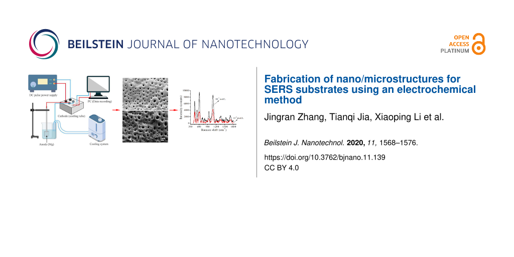
As-cast Mg ingots were sliced into rectangular coupons (15 × 15 × 4 mm3) for anodic oxidation treatment. Prior to the treatment, all specimens were ground using SiC paper up to 1200 grit, and then degreased with ethanol and deionized water in succession. No further purification was carried out. A customized DC power supply was used to conduct the PEO. Figure 1 shows the schematic diagram of nanopore formation using PEO processing. The specimens and carbon tubes were utilized as the anode and cathode, respectively, and the electrolyte solution was prepared with 2 g/L KOH and 10 g/L Na3PO4 in deionized water. The PEO treatment was performed in constant-current mode with a fixed constant current density of 25 mA/cm2. The frequency and duty ratio were 500 Hz and 50%, respectively. The electrolyte temperature was regulated within 30 ± 2 °C by a mechanical stirring cooling system. To study the influence of surface conditions (e.g., porosity and roughness) on the SERS intensity, the duration of the PEO treatment was set as the single variable (1, 2, and 5 min), as shown in Table 1.
![[2190-4286-11-139-1]](/bjnano/content/figures/2190-4286-11-139-1.jpg?scale=2.0&max-width=1024&background=FFFFFF)
Figure 1: Schematic diagram of fabrication of the nanopores substrates using PEO processing.
Figure 1: Schematic diagram of fabrication of the nanopores substrates using PEO processing.
Table 1: Parameters used for nanopore fabrication on the Mg surface using the PEO method.
| Condition | Parameter |
|---|---|
| Material | SiC-polished Mg ingot |
| Solution |
2 g/L KOH
and 10 g/L Na3PO4 |
| Treatment method | Plasma electrolytic oxidation (PEO) |
| Electric current parameter |
Constant current density 25 mA/cm2
Duty ratio 50% Frequency 500 Hz |
| Temperature | 30 ± 2 °C |
| Preparation time |
1 min
2 min 5 min |
The structured Mg surfaces were coated with Au of varying thickness and dipped into an aqueous solution of R6G (10−7 mol·L−1) for 20 min. The excess R6G molecules were removed by rinsing with ethanol and a gentle nitrogen flow was used to dry the samples.
A micro-Raman inVia spectroscopic system (Renishaw, UK) with 532 and 785 nm lasers was used. The incident optical power was kept at 0.6 mW with a 50× objective and the beam diameter was approx. 1 μm. The signal detector used a CCD camera (1040 × 256 pixels) with a grating size of 1800 lines/mm. The exposure time was 1 s and one accumulation scan was employed. The mapping images of the Raman spectrum were scanned over a 20 × 20 μm2 area. Before the tests, the Raman spectra were rectified using a standard Si substrate. A Raman intensity peak of 1362 cm−1 for R6G was chosen in the experiment.
An atomic force microscopy (AFM) system (Dimension Icon, Bruker, Germany) was employed to detect the two-dimensional and three-dimensional topographies of the nanopores. Imaging was performed in contact mode and an elastic constant of 0.2 N/m was selected for the silicon cantilever. The scanning area was 50 × 50 μm2. In addition, a scanning electron microscopy (SEM) system (Zeiss, Germany) was employed to characterize the nanopores.
Results and Discussion
Fabrication of arrayed nanopores on the Mg surface
Surface roughness and chemical composition have a strong influence on the intensity of Raman signals. PEO was employed to fabricate a porous oxide layer on a Mg alloy surface, which benefits from the increase of surface roughness and shows the potential for storing micro- or nanoparticles. During PEO treatment, the intrinsic passivation layer of the Mg alloy is disrupted in random positions through local melting during electrical breakdowns. After cooling by the electrolyte, a stable oxide layer containing arrayed pores is deposited on the surface. The parameters and duration of the PEO process should be carefully determined, as intensive energy input and longer treatment duration may create excessive surface roughness or even introduce unexpected defects on the surface. Thus, a set of moderate parameters was applied in this work to ensure that the Raman signal reflection properties were optimal.
Figure 2 shows the two-dimensional topographies of the arrayed nanopores with different treatment time of 1, 2, and 5 min. Figure 2a shows the two-dimensional topographies of the arrayed nanopores after 1 min of treatment time. The depth and diameter of the nanopores gradually increased as the treatment time increased, as shown in Figure 2b,c. Figure 2d shows cross-sectional SEM images of arrayed nanopores. The surface morphology includes MgO and Mg layers. In addition, a clamp is used to fix the sample. As shown in Figure 2, all PEO-treated Mg specimens demonstrate the typical surface morphology, which comprises of micrometer and sub-micrometer-sized quasi-circular pores and cracks. This porous and uneven surface is a result of the consecutive dielectric breakdown of the passivation layer and the heat generated during that process. As a result, the average diameter of the pores increases as the duration of PEO duration increases.
![[2190-4286-11-139-2]](/bjnano/content/figures/2190-4286-11-139-2.jpg?scale=2.0&max-width=1024&background=FFFFFF)
Figure 2: SEM images of the arrayed nanopores after different treatment times. SEM image of the arrayed nanopores after the treatment times of (a) 1 min, (b) 2 min, and (c) 5 min. (d) Cross-sectional SEM image of arrayed nanopores.
Figure 2: SEM images of the arrayed nanopores after different treatment times. SEM image of the arrayed nanop...
Figure 3 shows AFM images of the arrayed nanopores after fabrication with different treatment times. After 1 min, the nanopore diameter and depth were 0.7 ± 0.25 µm and 0.5 ± 0.16 µm, respectively (Figure 3a). After 2 min, the nanopore diameter and depth were 0.9 ± 0.3 µm and 0.6 ± 0.15 µm (Figure 3b). When the treatment time was increased to 5 min, the nanopore diameter and depth were 1.5 ± 0.3 µm and 1 ± 0.1 µm, respectively, as shown in Figure 3c. When the treatment time was increased to 10 min, the nanopore diameter and depth were 7.2 ± 0.3 µm and 5 ± 0.5 µm, respectively, as shown in Figure 3d. Thus, a 10 min treatment time led to the formation of pores with microscale structure. A three-dimensional AFM image of arrayed nanopores after a treatment time of 5 min is shown in Figure 3e.
![[2190-4286-11-139-3]](/bjnano/content/figures/2190-4286-11-139-3.jpg?scale=2.0&max-width=1024&background=FFFFFF)
Figure 3: AFM images of the arrayed nanopores with different treatment time. AFM image of the arrayed nanopores after a treatment time of (a) 1 min, (b) 2 min, (c) 5 min, and (d) 10 min. (e) Three-dimensional AFM image of arrayed nanopores after a treatment time of 5 min (e).
Figure 3: AFM images of the arrayed nanopores with different treatment time. AFM image of the arrayed nanopor...
Structurally similar nanopores can be machined by using mechanical machining methods. For instance, micro/nanostructures can be fabricated using diamond turning, such as single point diamond turning or diamond fly cutting. For example, sinusoidal grid surfaces can be formed with the aid of fast tool servos. Nanopores with depths of 6.33 µm can be generated by using diamond turning [44].
Raman intensity of R6G molecules on the arrayed nanopores
The PEO treatment time and the thickness of the Au film can have a significant impact on the performance of the SERS substrate. The performance was quantified by measuring Raman enhancement, which was determined by using R6G as a probe molecule.
Raman intensity with different thicknesses of the gold film
The effect of Raman enhancement of R6G molecules with different thicknesses of the gold film on the same structure surface (10, 20, and 30 nm) was studied. The data of Raman mapping were exported from the Raman spectra point by point.
Figure 4 shows the Raman spectra of R6G molecules (10−7 M) on nanopore substrates coated with different thicknesses of the Au film after a constant time of PEO treatment (5 min). The characteristic Raman peaks of R6G molecules were detected at 611, 772, 1183, 1311, 1362, 1503, and 1605 cm−1. The results indicate that the Raman signal was most intense when the nanopore substrate with a 10 nm thick Au film was used. The Raman intensity of R6G decreased as the thickness of the Au film increased. Accordingly, the Raman intensity of the R6G signal derived from substrates coated with a 30 nm thick Au film was very low, as shown in Figure 4. Overall, the results show that the Raman intensity of R6G is affected by the thickness of the Au film. The effect of Au thickness on the electric field intensity has previously been studied [45-47]. Zhang et al. [45] used a self-assembled method to fabricate PS nanosphere array substrates with Ag films of different thickness. The strongest electric field intensity enhancement was generated with a 10 nm thick Ag film. Using the AFM-based scratching method, Wang et al. [46] obtained nanodot array structures fabricated with Au films of different thickness. The Au were 13, 20, and 40 nm thick. The results show that a 13 nm thick Au film conferred the best enhancement effect. Therefore, the use of a thinner Au film can improve the Raman intensity of probe molecules. Cao et al. [47] employed femtosecond laser irradiation to fabricate nanorod arrayed structures decorated with Au nanoparticles. The study showed that the Raman intensity tended to decrease as the Au film thickness increased. Based on the above results, we selected Au films of 10 nm thickness for further quantification of the Raman intensity of probe molecules.
![[2190-4286-11-139-4]](/bjnano/content/figures/2190-4286-11-139-4.png?scale=2.0&max-width=1024&background=FFFFFF)
Figure 4: Raman spectra of R6G molecules (10−7 M) measured using Au-coated nanopore substrates with Au film thicknesses of 10, 20, and 30 nm.
Figure 4: Raman spectra of R6G molecules (10−7 M) measured using Au-coated nanopore substrates with Au film t...
Raman intensity after different treatment times
Figure 5 shows the Raman spectra of R6G molecules (10−7 mol·L−1) on nanopore structures that were fabricated using PEO different treatment times. The microstructures vary in their morphology depending to the length of the treatment time, which in turn has a profound effect on the Raman intensity. Compared with other structures generated using different treatment times, a bare surface did not yield a high Raman intensity when measuring R6G. The Raman intensity was strongest when surfaces were PEO-treated for 1 min and a Au film of 10 nm thickness was deposited (Figure 5 and Figure 2a). Under these conditions nanopores with smaller dimensions were formed than after treatment times of 2 and 5 min. The Raman intensity of R6G molecules was three-fold higher after a treatment time of 1 min than after treatment times of 2 and 5 min.
![[2190-4286-11-139-5]](/bjnano/content/figures/2190-4286-11-139-5.png?scale=2.0&max-width=1024&background=FFFFFF)
Figure 5: Raman spectra of R6G molecules (10−7 M) after different PEO treatment times (1, 2, and 5 min).
Figure 5: Raman spectra of R6G molecules (10−7 M) after different PEO treatment times (1, 2, and 5 min).
A single-cavity structure can significantly enhance the Raman signal [48-50]. Chang et al. [48] fabricated cavities by using an indentation method and found that the Raman intensities of R6G were influenced by indentation depth and tip-to-tip displacement. In our previous studies [49,50], a cavity depth of 1.7 µm was generated using a normal force of 10 mN with the force modulation indentation method. However, nanocavities were formed by the overlap of adjacent cavities. The depth of the nanocavities reached ca. 200 nm as the machining feeds were reduced. In addition, the Raman intensity reported by the R6G probe on the nanostructures was ten times that of a single-cavity structure.
Figure 6 shows the Raman intensity mapping image of arrayed nanopores formed after a treatment time of 2 min with a Au coating of 10 nm thickness. The Raman signal of R6G molecules could be detected. Thus, the electrochemical method can be used to create flexible Au-coated substrates of highly reproducible structure with long-term stability.
![[2190-4286-11-139-6]](/bjnano/content/figures/2190-4286-11-139-6.png?scale=2.0&max-width=1024&background=FFFFFF)
Figure 6: Raman intensity mapping image of arrayed nanopores formed after a treatment time of 2 min with a Au coating of 10 nm thickness.
Figure 6: Raman intensity mapping image of arrayed nanopores formed after a treatment time of 2 min with a Au...
SERS measurement of lysozyme on the nanopore substrates
The enzyme lysozyme can rupture the cell walls of certain pathogens following activation of the innate immune system [51]. However, excess lysozyme activity can increase the incidence of some diseases. In certain kinds of cancer, such as leukemia [52], excessive production of lysozyme is toxic and can induce organ disorder.
Figure 7 shows the SERS spectra of lysozyme (10−6 mol·L−1 and 10−5 mol·L−1) in ethanol solution on nanopore substrates that were fabricated with a PEO treatment time of 1 min and were coated with a Au film of 10 nm thickness. The characteristic Raman peaks of lysozyme molecules were detected at concentrations as low as 10−6 mol·L−1. These peaks included SS bridge (521 cm−1), phenylalanine (601 cm−1), tryptophan(s) (760 cm−1), tyrosine doublet (858 cm−1), tryptophan (881 cm−1), CC stretching (934 cm−1), tyrosine (1085 cm−1, 1210 cm−1), tryptophan (1337 cm−1), COO− symmetric stretch(s) (1384 cm−1), and tryptophan (1554 cm−1). Together, these data show that the electrochemical method can be used to fabricate nanopores as SERS substrates for the sensitive detection of proteins such as lysozyme.
![[2190-4286-11-139-7]](/bjnano/content/figures/2190-4286-11-139-7.png?scale=2.0&max-width=1024&background=FFFFFF)
Figure 7: Raman spectra of lysozyme molecules of 10−6 mol·L−1 and 10−5 mol·L−1 on nanopore substrates fabricated with a treatment time of 1 min and coated with a 10 nm Au film.
Figure 7: Raman spectra of lysozyme molecules of 10−6 mol·L−1 and 10−5 mol·L−1 on nanopore substrates fabrica...
Conclusion
Two- and three-dimensional arrayed micro/nanopores can be machined on Mg substrates by using a novel electrochemical method. The optimal treatment time for the process was 1 min, and the SERS intensity of the R6G molecules was enhanced by applying a 10 nm Au film onto the structured Mg surface. The SERS enhancement factor of this optimized system was between 106 and 1.75 × 10⁷. Experiments with lysozyme demonstrated that the Mg–Au nanopore substrates can be used to detect low levels of proteins (10−6 mol·L−1). Due to its reliability, homogeneity, low cost and high sensitivity, the system described herein holds great promise for future protein detection and quantification applications.
Funding
Jingran Zhang acknowledges the National Natural Science Foundation of China (grant No. 51905047), the China Postdoctoral Science Foundation (grant No. 2020M670824), the Jilin Postdoctoral Science Foundation and The Education Department of Jilin Province (grant No. JJKH20200750KJ). Junjie Yang acknowledges the Fundamental Research Funds for the Central Universities (grand No. 21620342) and National Key Research and Development Project (grand No. 2020YFC1107202).
References
-
Ma, D.; Huang, C.; Zheng, J.; Tang, J.; Li, J.; Yang, J.; Yang, R. Biosens. Bioelectron. 2018, 101, 167–173. doi:10.1016/j.bios.2017.08.062
Return to citation in text: [1] -
Deng, Z.; Wen, P.; Wang, N.; Peng, B. Sens. Actuators, B 2019, 288, 20–26. doi:10.1016/j.snb.2019.02.068
Return to citation in text: [1] -
Deng, Z.-Y.; Chen, K.-L.; Wu, C.-H. Sci. Rep. 2019, 9, 9566. doi:10.1038/s41598-019-45879-5
Return to citation in text: [1] -
Naqvi, T. K.; Sree Satya Bharati, M.; Srivastava, A. K.; Kulkarni, M. M.; Siddiqui, A. M.; Rao, S. V.; Dwivedi, P. K. ACS Omega 2019, 4, 17691–17701. doi:10.1021/acsomega.9b01975
Return to citation in text: [1] -
Byram, C.; Moram, S. S. B.; Soma, V. R. Analyst 2019, 144, 2327–2336. doi:10.1039/c8an01276h
Return to citation in text: [1] -
Liszewska, M.; Bartosewicz, B.; Budner, B.; Nasiłowska, B.; Szala, M.; Weyher, J. L.; Dzięcielewski, I.; Mierczyk, Z.; Jankiewicz, B. J. Vib. Spectrosc. 2018, 100, 79–85. doi:10.1016/j.vibspec.2018.11.002
Return to citation in text: [1] -
Sivashanmugan, K.; Lee, H.; Syu, C.-H.; Liu, B. H.-C.; Liao, J.-D. J. Taiwan Inst. Chem. Eng. 2017, 75, 287–291. doi:10.1016/j.jtice.2017.03.022
Return to citation in text: [1] -
Lin, S.; Hasi, W.; Han, S.; Lin, X.; Wang, L. Anal. Methods 2020, 12, 2571–2579. doi:10.1039/d0ay00483a
Return to citation in text: [1] -
Liang, P.; Cao, Y.; Dong, Q.; Wang, D.; Zhang, D.; Jin, S.; Yu, Z.; Ye, J.; Zou, M. Microchim. Acta 2020, 187, 335. doi:10.1007/s00604-020-04303-w
Return to citation in text: [1] -
Pham, T. B. N.; Bui, T. T. T.; Tran, V. Q.; Dang, V. Q.; Hoang, L. N.; Tran, C. K. Appl. Nanosci. 2020, 10, 703–714. doi:10.1007/s13204-019-01154-7
Return to citation in text: [1] -
Štolcová, L.; Peksa, V.; Proška, J.; Procházka, M. J. Raman Spectrosc. 2017, 49, 499–505. doi:10.1002/jrs.5317
Return to citation in text: [1] -
Sarkar, D.; Khare, D.; Kaushal, A.; Acharya, C.; Bahadur, J.; Prakash, J.; Donthula, H.; Dasgupta, K. Appl. Nanosci. 2019, 9, 1925–1937. doi:10.1007/s13204-019-01031-3
Return to citation in text: [1] -
Wang, J.; Yan, Y.; Chang, S.; Han, Y.; Geng, Y. Appl. Surf. Sci. 2020, 509, 145332. doi:10.1016/j.apsusc.2020.145332
Return to citation in text: [1] -
Jiang, H.; Li, J.; Cao, C.; Liu, X.; Liu, M.; Shen, Y.; Liu, Y.; Zhang, Q.; Wang, W.; Gu, L.; Sun, B. Nano Res. 2019, 12, 2808–2814. doi:10.1007/s12274-019-2517-2
Return to citation in text: [1] -
Matricardi, C.; Hanske, C.; Garcia-Pomar, J. L.; Langer, J.; Mihi, A.; Liz-Marzán, L. M. ACS Nano 2018, 12, 8531–8539. doi:10.1021/acsnano.8b04073
Return to citation in text: [1] -
Alsammarraie, F. K.; Lin, M. J. Agric. Food Chem. 2017, 65, 666–674. doi:10.1021/acs.jafc.6b04774
Return to citation in text: [1] -
Gopalakrishnan, A.; Chirumamilla, M.; De Angelis, F.; Toma, A.; Zaccaria, R. P.; Krahne, R. ACS Nano 2014, 8, 7986–7994. doi:10.1021/nn5020038
Return to citation in text: [1] -
Chirumamilla, M.; Gopalakrishnan, A.; Toma, A.; Proietti Zaccaria, R.; Krahne, R. Nanotechnology 2014, 25, 235303. doi:10.1088/0957-4484/25/23/235303
Return to citation in text: [1] -
Huck, C.; Toma, A.; Neubrech, F.; Chirumamilla, M.; Vogt, J.; De Angelis, F.; Pucci, A. ACS Photonics 2015, 2, 497–505. doi:10.1021/ph500374r
Return to citation in text: [1] -
Yockell-Lelièvre, H.; Lussier, F.; Masson, J.-F. J. Phys. Chem. C 2015, 119, 28577–28585. doi:10.1021/acs.jpcc.5b09570
Return to citation in text: [1] -
Scholes, F. H.; Davis, T. J.; Vernon, K. C.; Lau, D.; Furman, S. A.; Glenn, A. M. J. Raman Spectrosc. 2012, 43, 196–201. doi:10.1002/jrs.3034
Return to citation in text: [1] [2] -
Mabbott, S.; Xu, Y.; Goodacre, R. Anal. Methods 2017, 9, 4783–4789. doi:10.1039/c7ay01584d
Return to citation in text: [1] [2] -
Zhu, S.; Fan, C.; Wang, J.; Liang, E.; Hao, H. Spectrosc. Lett. 2018, 51, 453–461. doi:10.1080/00387010.2018.1503603
Return to citation in text: [1] [2] -
Candeloro, P.; Iuele, E.; Perozziello, G.; Coluccio, M. L.; Gentile, F.; Malara, N.; Mollace, V.; Di Fabrizio, E. Microelectron. Eng. 2017, 175, 30–33. doi:10.1016/j.mee.2016.12.015
Return to citation in text: [1] [2] -
Yue, W.; Wang, Z.; Yang, Y.; Chen, L.; Syed, A.; Wong, K.; Wang, X. J. Micromech. Microeng. 2012, 22, 125007. doi:10.1088/0960-1317/22/12/125007
Return to citation in text: [1] [2] -
Wu, T.; Lin, Y.-W. Appl. Surf. Sci. 2018, 435, 1143–1149. doi:10.1016/j.apsusc.2017.11.213
Return to citation in text: [1] [2] -
Min, Q.; Santos, M. J. L.; Girotto, E. M.; Brolo, A. G.; Gordon, R. J. Phys. Chem. C 2008, 112, 15098–15101. doi:10.1021/jp806785u
Return to citation in text: [1] -
Brolo, A. G.; Arctander, E.; Gordon, R.; Leathem, B.; Kavanagh, K. L. Nano Lett. 2004, 4, 2015–2018. doi:10.1021/nl048818w
Return to citation in text: [1] -
Lin, Y.-Y.; Liao, J.-D.; Ju, Y.-H.; Chang, C.-W.; Shiau, A.-L. Nanotechnology 2011, 22, 185308. doi:10.1088/0957-4484/22/18/185308
Return to citation in text: [1] [2] -
Gao, T.; Xu, Z.; Fang, F.; Gao, W.; Zhang, Q.; Xu, X. Nanoscale Res. Lett. 2012, 7, 399. doi:10.1186/1556-276x-7-399
Return to citation in text: [1] [2] -
Gao, H.; Hyun, J. K.; Lee, M. H.; Yang, J.-C.; Lauhon, L. J.; Odom, T. W. Nano Lett. 2010, 10, 4111–4116. doi:10.1021/nl1022892
Return to citation in text: [1] -
Sivashanmugan, K.; Liao, J.-D.; You, J.-W.; Wu, C.-L. Sens. Actuators, B 2013, 181, 361–367. doi:10.1016/j.snb.2013.01.035
Return to citation in text: [1] [2] -
Gao, T.; Xu, Z.; Fang, F.; Gao, W.; Zhang, Q.; Xu, X. Nanoscale Res. Lett. 2012, 7, 399. doi:10.1186/1556-276x-7-399
Return to citation in text: [1] [2] -
Yang, K.-H.; Chang, C.-M. Mater. Res. Bull. 2013, 48, 372–377. doi:10.1016/j.materresbull.2012.10.040
Return to citation in text: [1] [2] -
Chang, C.-C.; Yang, K.-H.; Liu, Y.-C.; Yu, C.-C. Anal. Chim. Acta 2012, 709, 91–97. doi:10.1016/j.aca.2011.10.017
Return to citation in text: [1] [2] -
Yang, K.-H.; Liu, Y.-C.; Yu, C.-C. Langmuir 2010, 26, 11512–11517. doi:10.1021/la100235x
Return to citation in text: [1] [2] -
Chen, H.-C.; Chen, C.-H.; Hsu, C.-S.; Chen, T.-L.; Liao, M.-Y.; Wang, C.-C.; Tsai, C.-F.; Chen, H. M. ACS Omega 2018, 3, 16576–16584. doi:10.1021/acsomega.8b02677
Return to citation in text: [1] [2] -
Ou, K.-L.; Hsu, T.-C.; Liu, Y.-C.; Yang, K.-H. Mater. Chem. Phys. 2012, 135, 892–896. doi:10.1016/j.matchemphys.2012.05.075
Return to citation in text: [1] [2] -
Piergies, N.; Kim, Y.; Proniewicz, E. Vib. Spectrosc. 2016, 83, 94–100. doi:10.1016/j.vibspec.2016.01.012
Return to citation in text: [1] -
Celik, M.; Altuntas, S.; Buyukserin, F. Sens. Actuators, B 2018, 255, 2871–2877. doi:10.1016/j.snb.2017.09.105
Return to citation in text: [1] -
Han, Y.; Wang, H.; Qiang, L.; Gao, Y.; Li, Q.; Pang, J.; Liu, H.; Han, L.; Wu, Y.; Zhang, Y. J. Mater. Sci. 2020, 55, 591–602. doi:10.1007/s10853-019-04036-z
Return to citation in text: [1] [2] -
Choi, D.; Choi, Y.; Hong, S.; Kang, T.; Lee, L. P. Small 2010, 6, 1741–1744. doi:10.1002/smll.200901937
Return to citation in text: [1] [2] -
Lin, B.; Kannan, P.; Qiu, B.; Lin, Z.; Guo, L. Food Chem. 2020, 307, 125528. doi:10.1016/j.foodchem.2019.125528
Return to citation in text: [1] [2] -
Cheng, K.; Huo, D., Eds. Micro-Cutting: Fundamentals and Applications; John Wiley & Sons Ltd: Chichester, UK, 2013. doi:10.1002/9781118536605
Return to citation in text: [1] -
Zhang, W.; Xue, T.; Zhang, L.; Lu, F.; Liu, M.; Meng, C.; Mao, D.; Mei, T. Sensors 2019, 19, 3966. doi:10.3390/s19183966
Return to citation in text: [1] [2] -
Wang, J.; Yan, Y.; Chang, S.; Han, Y.; Geng, Y. Appl. Surf. Sci. 2020, 509, 145332. doi:10.1016/j.apsusc.2020.145332
Return to citation in text: [1] [2] -
Cao, W.; Jiang, L.; Hu, J.; Wang, A.; Li, X.; Lu, Y. ACS Appl. Mater. Interfaces 2018, 10, 1297–1305. doi:10.1021/acsami.7b13241
Return to citation in text: [1] [2] -
Chang, C.-W.; Liao, J.-D.; Shiau, A.-L.; Yao, C.-K. Sens. Actuators, B 2011, 156, 471–478. doi:10.1016/j.snb.2011.04.006
Return to citation in text: [1] [2] -
Yan, Y.; Zhang, J.; Xu, P.; Miao, P. RSC Adv. 2017, 7, 11969–11978. doi:10.1039/c6ra28875h
Return to citation in text: [1] [2] -
Zhang, J.; Jia, T.; Yan, Y.; Wang, L.; Miao, P.; Han, Y.; Zhang, X.; Shi, G.; Geng, Y.; Weng, Z.; Laipple, D.; Wang, Z. Beilstein J. Nanotechnol. 2019, 10, 2483–2496. doi:10.3762/bjnano.10.239
Return to citation in text: [1] [2] -
Saurabh, S.; Sahoo, P. K. Aquacult. Res. 2008, 39, 223–239. doi:10.1111/j.1365-2109.2007.01883.x
Return to citation in text: [1] -
Krugliak, L.; Meyer, P. R.; Taylor, C. R. Am. J. Hematol. 1986, 21, 99–109. doi:10.1002/ajh.2830210112
Return to citation in text: [1]
| 45. | Zhang, W.; Xue, T.; Zhang, L.; Lu, F.; Liu, M.; Meng, C.; Mao, D.; Mei, T. Sensors 2019, 19, 3966. doi:10.3390/s19183966 |
| 46. | Wang, J.; Yan, Y.; Chang, S.; Han, Y.; Geng, Y. Appl. Surf. Sci. 2020, 509, 145332. doi:10.1016/j.apsusc.2020.145332 |
| 47. | Cao, W.; Jiang, L.; Hu, J.; Wang, A.; Li, X.; Lu, Y. ACS Appl. Mater. Interfaces 2018, 10, 1297–1305. doi:10.1021/acsami.7b13241 |
| 45. | Zhang, W.; Xue, T.; Zhang, L.; Lu, F.; Liu, M.; Meng, C.; Mao, D.; Mei, T. Sensors 2019, 19, 3966. doi:10.3390/s19183966 |
| 46. | Wang, J.; Yan, Y.; Chang, S.; Han, Y.; Geng, Y. Appl. Surf. Sci. 2020, 509, 145332. doi:10.1016/j.apsusc.2020.145332 |
| 1. | Ma, D.; Huang, C.; Zheng, J.; Tang, J.; Li, J.; Yang, J.; Yang, R. Biosens. Bioelectron. 2018, 101, 167–173. doi:10.1016/j.bios.2017.08.062 |
| 2. | Deng, Z.; Wen, P.; Wang, N.; Peng, B. Sens. Actuators, B 2019, 288, 20–26. doi:10.1016/j.snb.2019.02.068 |
| 3. | Deng, Z.-Y.; Chen, K.-L.; Wu, C.-H. Sci. Rep. 2019, 9, 9566. doi:10.1038/s41598-019-45879-5 |
| 12. | Sarkar, D.; Khare, D.; Kaushal, A.; Acharya, C.; Bahadur, J.; Prakash, J.; Donthula, H.; Dasgupta, K. Appl. Nanosci. 2019, 9, 1925–1937. doi:10.1007/s13204-019-01031-3 |
| 13. | Wang, J.; Yan, Y.; Chang, S.; Han, Y.; Geng, Y. Appl. Surf. Sci. 2020, 509, 145332. doi:10.1016/j.apsusc.2020.145332 |
| 14. | Jiang, H.; Li, J.; Cao, C.; Liu, X.; Liu, M.; Shen, Y.; Liu, Y.; Zhang, Q.; Wang, W.; Gu, L.; Sun, B. Nano Res. 2019, 12, 2808–2814. doi:10.1007/s12274-019-2517-2 |
| 32. | Sivashanmugan, K.; Liao, J.-D.; You, J.-W.; Wu, C.-L. Sens. Actuators, B 2013, 181, 361–367. doi:10.1016/j.snb.2013.01.035 |
| 10. | Pham, T. B. N.; Bui, T. T. T.; Tran, V. Q.; Dang, V. Q.; Hoang, L. N.; Tran, C. K. Appl. Nanosci. 2020, 10, 703–714. doi:10.1007/s13204-019-01154-7 |
| 11. | Štolcová, L.; Peksa, V.; Proška, J.; Procházka, M. J. Raman Spectrosc. 2017, 49, 499–505. doi:10.1002/jrs.5317 |
| 33. | Gao, T.; Xu, Z.; Fang, F.; Gao, W.; Zhang, Q.; Xu, X. Nanoscale Res. Lett. 2012, 7, 399. doi:10.1186/1556-276x-7-399 |
| 7. | Sivashanmugan, K.; Lee, H.; Syu, C.-H.; Liu, B. H.-C.; Liao, J.-D. J. Taiwan Inst. Chem. Eng. 2017, 75, 287–291. doi:10.1016/j.jtice.2017.03.022 |
| 8. | Lin, S.; Hasi, W.; Han, S.; Lin, X.; Wang, L. Anal. Methods 2020, 12, 2571–2579. doi:10.1039/d0ay00483a |
| 9. | Liang, P.; Cao, Y.; Dong, Q.; Wang, D.; Zhang, D.; Jin, S.; Yu, Z.; Ye, J.; Zou, M. Microchim. Acta 2020, 187, 335. doi:10.1007/s00604-020-04303-w |
| 29. | Lin, Y.-Y.; Liao, J.-D.; Ju, Y.-H.; Chang, C.-W.; Shiau, A.-L. Nanotechnology 2011, 22, 185308. doi:10.1088/0957-4484/22/18/185308 |
| 51. | Saurabh, S.; Sahoo, P. K. Aquacult. Res. 2008, 39, 223–239. doi:10.1111/j.1365-2109.2007.01883.x |
| 4. | Naqvi, T. K.; Sree Satya Bharati, M.; Srivastava, A. K.; Kulkarni, M. M.; Siddiqui, A. M.; Rao, S. V.; Dwivedi, P. K. ACS Omega 2019, 4, 17691–17701. doi:10.1021/acsomega.9b01975 |
| 5. | Byram, C.; Moram, S. S. B.; Soma, V. R. Analyst 2019, 144, 2327–2336. doi:10.1039/c8an01276h |
| 6. | Liszewska, M.; Bartosewicz, B.; Budner, B.; Nasiłowska, B.; Szala, M.; Weyher, J. L.; Dzięcielewski, I.; Mierczyk, Z.; Jankiewicz, B. J. Vib. Spectrosc. 2018, 100, 79–85. doi:10.1016/j.vibspec.2018.11.002 |
| 30. | Gao, T.; Xu, Z.; Fang, F.; Gao, W.; Zhang, Q.; Xu, X. Nanoscale Res. Lett. 2012, 7, 399. doi:10.1186/1556-276x-7-399 |
| 52. | Krugliak, L.; Meyer, P. R.; Taylor, C. R. Am. J. Hematol. 1986, 21, 99–109. doi:10.1002/ajh.2830210112 |
| 24. | Candeloro, P.; Iuele, E.; Perozziello, G.; Coluccio, M. L.; Gentile, F.; Malara, N.; Mollace, V.; Di Fabrizio, E. Microelectron. Eng. 2017, 175, 30–33. doi:10.1016/j.mee.2016.12.015 |
| 26. | Wu, T.; Lin, Y.-W. Appl. Surf. Sci. 2018, 435, 1143–1149. doi:10.1016/j.apsusc.2017.11.213 |
| 48. | Chang, C.-W.; Liao, J.-D.; Shiau, A.-L.; Yao, C.-K. Sens. Actuators, B 2011, 156, 471–478. doi:10.1016/j.snb.2011.04.006 |
| 21. | Scholes, F. H.; Davis, T. J.; Vernon, K. C.; Lau, D.; Furman, S. A.; Glenn, A. M. J. Raman Spectrosc. 2012, 43, 196–201. doi:10.1002/jrs.3034 |
| 22. | Mabbott, S.; Xu, Y.; Goodacre, R. Anal. Methods 2017, 9, 4783–4789. doi:10.1039/c7ay01584d |
| 23. | Zhu, S.; Fan, C.; Wang, J.; Liang, E.; Hao, H. Spectrosc. Lett. 2018, 51, 453–461. doi:10.1080/00387010.2018.1503603 |
| 27. | Min, Q.; Santos, M. J. L.; Girotto, E. M.; Brolo, A. G.; Gordon, R. J. Phys. Chem. C 2008, 112, 15098–15101. doi:10.1021/jp806785u |
| 28. | Brolo, A. G.; Arctander, E.; Gordon, R.; Leathem, B.; Kavanagh, K. L. Nano Lett. 2004, 4, 2015–2018. doi:10.1021/nl048818w |
| 29. | Lin, Y.-Y.; Liao, J.-D.; Ju, Y.-H.; Chang, C.-W.; Shiau, A.-L. Nanotechnology 2011, 22, 185308. doi:10.1088/0957-4484/22/18/185308 |
| 30. | Gao, T.; Xu, Z.; Fang, F.; Gao, W.; Zhang, Q.; Xu, X. Nanoscale Res. Lett. 2012, 7, 399. doi:10.1186/1556-276x-7-399 |
| 31. | Gao, H.; Hyun, J. K.; Lee, M. H.; Yang, J.-C.; Lauhon, L. J.; Odom, T. W. Nano Lett. 2010, 10, 4111–4116. doi:10.1021/nl1022892 |
| 32. | Sivashanmugan, K.; Liao, J.-D.; You, J.-W.; Wu, C.-L. Sens. Actuators, B 2013, 181, 361–367. doi:10.1016/j.snb.2013.01.035 |
| 33. | Gao, T.; Xu, Z.; Fang, F.; Gao, W.; Zhang, Q.; Xu, X. Nanoscale Res. Lett. 2012, 7, 399. doi:10.1186/1556-276x-7-399 |
| 49. | Yan, Y.; Zhang, J.; Xu, P.; Miao, P. RSC Adv. 2017, 7, 11969–11978. doi:10.1039/c6ra28875h |
| 50. | Zhang, J.; Jia, T.; Yan, Y.; Wang, L.; Miao, P.; Han, Y.; Zhang, X.; Shi, G.; Geng, Y.; Weng, Z.; Laipple, D.; Wang, Z. Beilstein J. Nanotechnol. 2019, 10, 2483–2496. doi:10.3762/bjnano.10.239 |
| 21. | Scholes, F. H.; Davis, T. J.; Vernon, K. C.; Lau, D.; Furman, S. A.; Glenn, A. M. J. Raman Spectrosc. 2012, 43, 196–201. doi:10.1002/jrs.3034 |
| 22. | Mabbott, S.; Xu, Y.; Goodacre, R. Anal. Methods 2017, 9, 4783–4789. doi:10.1039/c7ay01584d |
| 23. | Zhu, S.; Fan, C.; Wang, J.; Liang, E.; Hao, H. Spectrosc. Lett. 2018, 51, 453–461. doi:10.1080/00387010.2018.1503603 |
| 24. | Candeloro, P.; Iuele, E.; Perozziello, G.; Coluccio, M. L.; Gentile, F.; Malara, N.; Mollace, V.; Di Fabrizio, E. Microelectron. Eng. 2017, 175, 30–33. doi:10.1016/j.mee.2016.12.015 |
| 25. | Yue, W.; Wang, Z.; Yang, Y.; Chen, L.; Syed, A.; Wong, K.; Wang, X. J. Micromech. Microeng. 2012, 22, 125007. doi:10.1088/0960-1317/22/12/125007 |
| 26. | Wu, T.; Lin, Y.-W. Appl. Surf. Sci. 2018, 435, 1143–1149. doi:10.1016/j.apsusc.2017.11.213 |
| 47. | Cao, W.; Jiang, L.; Hu, J.; Wang, A.; Li, X.; Lu, Y. ACS Appl. Mater. Interfaces 2018, 10, 1297–1305. doi:10.1021/acsami.7b13241 |
| 15. | Matricardi, C.; Hanske, C.; Garcia-Pomar, J. L.; Langer, J.; Mihi, A.; Liz-Marzán, L. M. ACS Nano 2018, 12, 8531–8539. doi:10.1021/acsnano.8b04073 |
| 16. | Alsammarraie, F. K.; Lin, M. J. Agric. Food Chem. 2017, 65, 666–674. doi:10.1021/acs.jafc.6b04774 |
| 17. | Gopalakrishnan, A.; Chirumamilla, M.; De Angelis, F.; Toma, A.; Zaccaria, R. P.; Krahne, R. ACS Nano 2014, 8, 7986–7994. doi:10.1021/nn5020038 |
| 18. | Chirumamilla, M.; Gopalakrishnan, A.; Toma, A.; Proietti Zaccaria, R.; Krahne, R. Nanotechnology 2014, 25, 235303. doi:10.1088/0957-4484/25/23/235303 |
| 19. | Huck, C.; Toma, A.; Neubrech, F.; Chirumamilla, M.; Vogt, J.; De Angelis, F.; Pucci, A. ACS Photonics 2015, 2, 497–505. doi:10.1021/ph500374r |
| 20. | Yockell-Lelièvre, H.; Lussier, F.; Masson, J.-F. J. Phys. Chem. C 2015, 119, 28577–28585. doi:10.1021/acs.jpcc.5b09570 |
| 25. | Yue, W.; Wang, Z.; Yang, Y.; Chen, L.; Syed, A.; Wong, K.; Wang, X. J. Micromech. Microeng. 2012, 22, 125007. doi:10.1088/0960-1317/22/12/125007 |
| 48. | Chang, C.-W.; Liao, J.-D.; Shiau, A.-L.; Yao, C.-K. Sens. Actuators, B 2011, 156, 471–478. doi:10.1016/j.snb.2011.04.006 |
| 49. | Yan, Y.; Zhang, J.; Xu, P.; Miao, P. RSC Adv. 2017, 7, 11969–11978. doi:10.1039/c6ra28875h |
| 50. | Zhang, J.; Jia, T.; Yan, Y.; Wang, L.; Miao, P.; Han, Y.; Zhang, X.; Shi, G.; Geng, Y.; Weng, Z.; Laipple, D.; Wang, Z. Beilstein J. Nanotechnol. 2019, 10, 2483–2496. doi:10.3762/bjnano.10.239 |
| 35. | Chang, C.-C.; Yang, K.-H.; Liu, Y.-C.; Yu, C.-C. Anal. Chim. Acta 2012, 709, 91–97. doi:10.1016/j.aca.2011.10.017 |
| 34. | Yang, K.-H.; Chang, C.-M. Mater. Res. Bull. 2013, 48, 372–377. doi:10.1016/j.materresbull.2012.10.040 |
| 35. | Chang, C.-C.; Yang, K.-H.; Liu, Y.-C.; Yu, C.-C. Anal. Chim. Acta 2012, 709, 91–97. doi:10.1016/j.aca.2011.10.017 |
| 36. | Yang, K.-H.; Liu, Y.-C.; Yu, C.-C. Langmuir 2010, 26, 11512–11517. doi:10.1021/la100235x |
| 37. | Chen, H.-C.; Chen, C.-H.; Hsu, C.-S.; Chen, T.-L.; Liao, M.-Y.; Wang, C.-C.; Tsai, C.-F.; Chen, H. M. ACS Omega 2018, 3, 16576–16584. doi:10.1021/acsomega.8b02677 |
| 38. | Ou, K.-L.; Hsu, T.-C.; Liu, Y.-C.; Yang, K.-H. Mater. Chem. Phys. 2012, 135, 892–896. doi:10.1016/j.matchemphys.2012.05.075 |
| 39. | Piergies, N.; Kim, Y.; Proniewicz, E. Vib. Spectrosc. 2016, 83, 94–100. doi:10.1016/j.vibspec.2016.01.012 |
| 34. | Yang, K.-H.; Chang, C.-M. Mater. Res. Bull. 2013, 48, 372–377. doi:10.1016/j.materresbull.2012.10.040 |
| 43. | Lin, B.; Kannan, P.; Qiu, B.; Lin, Z.; Guo, L. Food Chem. 2020, 307, 125528. doi:10.1016/j.foodchem.2019.125528 |
| 44. | Cheng, K.; Huo, D., Eds. Micro-Cutting: Fundamentals and Applications; John Wiley & Sons Ltd: Chichester, UK, 2013. doi:10.1002/9781118536605 |
| 41. | Han, Y.; Wang, H.; Qiang, L.; Gao, Y.; Li, Q.; Pang, J.; Liu, H.; Han, L.; Wu, Y.; Zhang, Y. J. Mater. Sci. 2020, 55, 591–602. doi:10.1007/s10853-019-04036-z |
| 42. | Choi, D.; Choi, Y.; Hong, S.; Kang, T.; Lee, L. P. Small 2010, 6, 1741–1744. doi:10.1002/smll.200901937 |
| 38. | Ou, K.-L.; Hsu, T.-C.; Liu, Y.-C.; Yang, K.-H. Mater. Chem. Phys. 2012, 135, 892–896. doi:10.1016/j.matchemphys.2012.05.075 |
| 40. | Celik, M.; Altuntas, S.; Buyukserin, F. Sens. Actuators, B 2018, 255, 2871–2877. doi:10.1016/j.snb.2017.09.105 |
| 41. | Han, Y.; Wang, H.; Qiang, L.; Gao, Y.; Li, Q.; Pang, J.; Liu, H.; Han, L.; Wu, Y.; Zhang, Y. J. Mater. Sci. 2020, 55, 591–602. doi:10.1007/s10853-019-04036-z |
| 42. | Choi, D.; Choi, Y.; Hong, S.; Kang, T.; Lee, L. P. Small 2010, 6, 1741–1744. doi:10.1002/smll.200901937 |
| 43. | Lin, B.; Kannan, P.; Qiu, B.; Lin, Z.; Guo, L. Food Chem. 2020, 307, 125528. doi:10.1016/j.foodchem.2019.125528 |
| 36. | Yang, K.-H.; Liu, Y.-C.; Yu, C.-C. Langmuir 2010, 26, 11512–11517. doi:10.1021/la100235x |
| 37. | Chen, H.-C.; Chen, C.-H.; Hsu, C.-S.; Chen, T.-L.; Liao, M.-Y.; Wang, C.-C.; Tsai, C.-F.; Chen, H. M. ACS Omega 2018, 3, 16576–16584. doi:10.1021/acsomega.8b02677 |
© 2020 Zhang et al.; licensee Beilstein-Institut.
This is an Open Access article under the terms of the Creative Commons Attribution License (https://creativecommons.org/licenses/by/4.0). Please note that the reuse, redistribution and reproduction in particular requires that the authors and source are credited.
The license is subject to the Beilstein Journal of Nanotechnology terms and conditions: (https://www.beilstein-journals.org/bjnano)