Abstract
The aim of this work is to determine the varying dielectric constant of a biological nanostructured system via electrostatic force microscopy (EFM) and to show how this method is useful to study natural photonic crystals. We mapped the dielectric constant of the cross section of the posterior wing of the damselfly Chalcopteryx rutilans with nanometric resolution. We obtained structural information on its constitutive nanolayers and the absolute values of their dielectric constant. By relating the measured profile of the static dielectric constant to the profile of the refractive index in the visible range, combined with optical reflectance measurements and simulation, we were able to describe the origin of the strongly iridescent wing colors of this Amazonian rainforest damselfly. The method we demonstrate here should be useful for the study of other biological nanostructured systems.
Introduction
The dielectric constant, or relative permittivity, is a fundamental physical property that is crucial for describing various biological, chemical, or physical phenomena. It is a material property associated to the decrease of the electric force between two point charges due to the medium. Therefore, it modulates the interaction between charged particles within materials and also the interaction of electromagnetic radiation with matter. Accordingly, it plays a fundamental role in fields such as the full understanding of proteins [1,2] or in the development of solar cells [3].
Natural photonic crystals are exciting nanostructured systems in which the dielectric properties play a fundamental role [4]. Many of them are biological systems where the richness of colors, produced by different strategies found in nature, is astonishing [5,6]. Studies of the origin of physical colors in insects are numerous in the literature and the most commonly used tools are non-local optical reflectance, electron microscopy, and scanning probe microscopy techniques, which give support to theoretical models aiming to describe the measured optical properties [7]. However, all these techniques directly reveal only the structure with nanometric resolution, the local dielectric response is indirectly inferred from a model [8-10]. Despite the large number of studies, the local dielectric properties of natural photonic crystals remain essentially undetermined due to the great difficulties in measuring the dielectric response at the nanometric scale [11]. The nanometric local relative permittivity of a natural photonic crystal has not been directly measured yet.
Fumagalli et al. [12-15], and Riedel et al. [16] developed several techniques of electrostatic force microscopy (EFM) to extract the relative permittivity at the nanoscale, allowing for new fields to be explored. Here we use EFM to map the relative permittivity of nanostructures within the wings of the Chalcopteryx rutilans damselfly [17-19]; nanostructures which make it a natural photonic crystal. We obtain quantitative information about the wing structure and its local relative permittivity values. We also simulate the optical reflectance using the extracted spatial profile of the relative permittivity and compare it with the measured reflectance in the visible range, obtaining a good correlation. In this way, we can provide a full description of the origin of the shimmering colors of the posterior wings of the Chalcopteryx rutilans damselfly male. This technique should be useful in the study of similar systems enhancing the investigation possibilities of natural photonic crystals.
Results and Discussion
In damselflies, color has many functions, the most important being sex recognition, courtship, and territory defense behavior [19]. In Chalcopteryx rutilans – a damselfly found in the Amazonian rain forest – those functions are performed by the male by displaying its strongly iridescent hind wings. The phenomenon of iridescence results from both diffraction and interference in the damselfly wings, and all observed colors result from a multilayer structure, that is, these wings are natural one-dimensional photonic crystals [7-10].
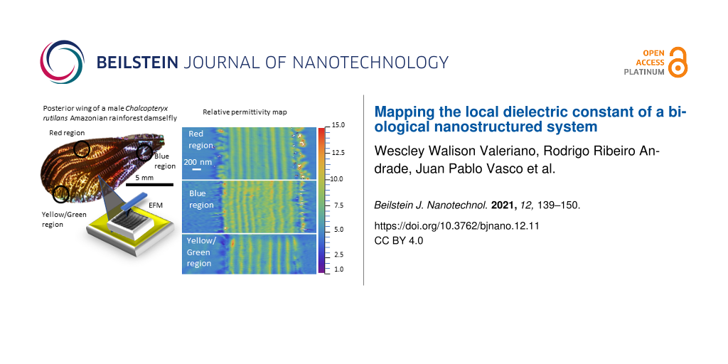
For our measurements, we chose three different color regions of the iridescent posterior wings of the male Chalcopteryx rutilans to study, that is, the yellow/green, red, and blue regions observed at the dorsal side, Figure 1a. The ventral side shows several shades of red, Figure 1b.
![[2190-4286-12-11-1]](/bjnano/content/figures/2190-4286-12-11-1.jpg?scale=2.0&max-width=1024&background=FFFFFF)
Figure 1: Optical images of the iridescent hind wing of the male damselfly Chalcopteryx rutilans (Rambur) (Odonata, Polythoridae). The dorsal side (a) displays colors that span all the visible wavelength spectrum. The image in (b) shows the ventral side, which is almost all red, remarkably similar to the iridescent wing of the female C. rutilans.
Figure 1: Optical images of the iridescent hind wing of the male damselfly Chalcopteryx rutilans (Rambur) (Od...
The scanning electron microscopy (SEM) image presented in Figure 2 shows the nanostructured section of a fragment of the red region indicated in Figure 1a. The section was partially polished using a focused ion beam (FIB) and the multilayered structure is clearly visible. The corrugated surface is the wax layer that covers the damselfly wings [20]. Detailed electron microscopy and mass spectrometry studies of this natural nanostructured system can be found in Valeriano [17] and Carr et al. [18].
![[2190-4286-12-11-2]](/bjnano/content/figures/2190-4286-12-11-2.jpg?scale=2.0&max-width=1024&background=FFFFFF)
Figure 2: SEM image of the cross section of a red region fragment of the Chalcopterix rutilans male rear wing. The smooth region was obtained by polishing using FIB.
Figure 2: SEM image of the cross section of a red region fragment of the Chalcopterix rutilans male rear wing...
Relative permittivity determination via EFM
The EFM measurements were performed in the conventional double-pass mode, which means that the probe executes two scans. The first scan measures the sample topography in tapping mode and the second scan mimics the profile at a defined lift height Zlift applying a voltage VDC between the tip and the conductive substrate [21].
The tip is mechanically forced to oscillate, during the second pass, at the resonance frequency of the cantilever, f0. Variations in the local relative permittivity properties of the sample will lead to different tip–sample force gradients, which promote a shift Δf0 in the tip oscillation frequency [21,22] which is, approximately,
![[2190-4286-12-11-i1]](/bjnano/content/inline/2190-4286-12-11-i1.svg?max-width=590&scale=1.18182)
where dF/dz is the tip–sample force gradient and K is the spring constant of the cantilever.
The tip–sample-substrate system constitutes a capacitor with the sample (wing) as part of the relative permittivity region, so the force between tip and substrate can be modeled as
![[2190-4286-12-11-i2]](/bjnano/content/inline/2190-4286-12-11-i2.svg?max-width=590&scale=1.18182)
where C is the system capacitance and VDC is the applied tip–sample bias.
From Equation 1 and Equation 2 we have:
![[2190-4286-12-11-i3]](/bjnano/content/inline/2190-4286-12-11-i3.svg?max-width=590&scale=1.18182)
This equation relates the frequency shift Δf0 to the applied bias voltage VDC and is the measured EFM signal. The bias-independent term in Equation 3 is defined as α, given by
![[2190-4286-12-11-i4]](/bjnano/content/inline/2190-4286-12-11-i4.svg?max-width=590&scale=1.18182)
Since f0, K and VDC are well determined, local variations of the measured frequency shift Δf0 are associated with changes in the second derivative of the capacitance in Equation 3 and Equation 4. The capacitance depends both on the geometry and on the relative permittivity of the medium. Hence, we only need to use a suitable capacitance model to be able to determine the local relative permittivity of the sample from the EFM data.
The capacitance model applied here considers a conical tip and an infinite flat surface with relative permittivity εr and thickness h, which has a capacitance expressed as
![[2190-4286-12-11-i5]](/bjnano/content/inline/2190-4286-12-11-i5.svg?max-width=590&scale=1.18182)
Inserting Equation 5 into Equation 4 leads to an expression from which the relative permittivity εr can be extracted:
![[2190-4286-12-11-i6]](/bjnano/content/inline/2190-4286-12-11-i6.svg?max-width=590&scale=1.18182)
where R is the tip apex radius, θ is the tip conical angle, z is the tip–sample distance, and h is the sample thickness. Figure 3 shows a scheme of the model, which is commonly applied for such a configuration [12-16].
![[2190-4286-12-11-3]](/bjnano/content/figures/2190-4286-12-11-3.png?scale=2.0&max-width=1024&background=FFFFFF)
Figure 3: Capacitance model with tip, sample, conductive plate, and the parameters used in our calculations. R is the tip apex radius, θ is the tip conical angle, z is the tip–sample distance, h is the sample thickness and εr is the relative permittivity of the sample. The sample is shown on top of the conductive substrate (yellow plate), which constitutes the bottom plate of the capacitor.
Figure 3: Capacitance model with tip, sample, conductive plate, and the parameters used in our calculations. R...
This capacitance model is valid under the following conditions: i) tip–sample distance z between 0 and 100 nm; ii) maximum sample thickness h around 100 nm; iii) relative permittivity εr smaller than 100; iv) nominal tip radius R between 30 and 200 nm; v) tip cone angle θ between 10° and 45° [12].
Determination of the coefficient α
For the experiments we use an atomic force microscope in the EFM mode, which measures the frequency shift for each bias voltage at each position of the sample. We varied the bias voltage from −10 V to +10 V, in steps of 1 V. Plotting the frequency shift as a function of the bias voltage, we obtain a parabolic function, as can be seen in Figure 4. Fitting the data with the function
![[2190-4286-12-11-i7]](/bjnano/content/inline/2190-4286-12-11-i7.svg?max-width=590&scale=1.18182)
where VSP is the tip–sample surface potential difference due to their different work functions [21], we obtain the coefficient α.
![[2190-4286-12-11-4]](/bjnano/content/figures/2190-4286-12-11-4.png?scale=2.0&max-width=1024&background=FFFFFF)
Figure 4: Frequency shift as a function of the bias voltage for the gold surface that is the conductive substrate in Figure 3, (orange squares) and for the blue region of the wing (blue circles). The fit using Equation 7 results in α(gold) = (6.37 ± 0.03) Hz/V2, and α(blue region) = (5.75 ± 0.04) Hz/V2.
Figure 4: Frequency shift as a function of the bias voltage for the gold surface that is the conductive subst...
Construction of the relative permittivity map
From the topographic image, the local thickness of the sample h is determined for each pixel, as we can see in Figure 5a.
![[2190-4286-12-11-5]](/bjnano/content/figures/2190-4286-12-11-5.jpg?scale=2.0&max-width=1024&background=FFFFFF)
Figure 5: (a) Topographic map; (b) α coefficient map; and (c) relative permittivity map. The average of all line profiles is shown below each image. All maps refer to the same red colored wing region.
Figure 5: (a) Topographic map; (b) α coefficient map; and (c) relative permittivity map. The average of all l...
EFM measurements were carried out in the same sample region, varying the bias voltage from −10 V to +10 V. This resulted in 21 images, each one an array of frequency shift values. For the same pixel element in the sample image, we have 21 pairs of values, that is, a frequency shift and its respective bias voltage. Through Equation 7 we obtain the α coefficient for each pixel element in the sample, Figure 5b.
The parameters in Equation 6, except the α coefficient and the thickness h, are the same for all pixel elements. Thus, solving the equation regarding the relative permittivity of each pixel, we construct a relative permittivity map as can be seen in Figure 5c and below in Figure 6. In the topographic map and the average profile, the different layers and their widths can be identified (Figure 5a). The α coefficient map and its average profile differ slightly from the topographic information, but some correspondences are identified. Thicker regions have a smaller α coefficient, as can be seen at the wing–resin interface (Figure 5b). There seems to be a correlation between topography (Figure 5a) and the relative permittivity εr (Figure 5c): the lower the topography, the larger the εr. However, we observe a small εr value in the lower topography regions adjacent to the wing slab. Hence, topography crosstalk is small.
Chalcopterix rutilans damselfly wings
Using the protocol described above, we constructed relative permittivity maps of the three color regions: red region (Figure 6a), blue region (Figure 6b), and yellow/green region (Figure 6c). The parameters used for the red region are f0 = 61.106 kHz, K = 1.19 N/m and R = (34.8 ± 0.2) nm; for the blue region they are f0 = 62.111 kHz, K = 1.87 N/m and R = (42.6 ± 0.2) nm; and for the yellow/green region the parameters are f0 = 67.972 kHz, K = 2.18 N/m and R = (35.9 ± 0.2) nm.
![[2190-4286-12-11-6]](/bjnano/content/figures/2190-4286-12-11-6.jpg?scale=2.0&max-width=1024&background=FFFFFF)
Figure 6: Relative permittivity image of three color regions of the hind wings of Chalcopterix rutilans: (a) red region, (b) blue region, and (c) yellow/green region. The color scale on the right side gives the values of the relative permittivity. On the left side, colored in purple, we have the Au/Cr surface. The areas that appear bluish in the images (εr around 4) correspond to the polymerized resin wrapping the wing. The wing slice lies between the white vertical dashed lines, which indicate the region where the profiles presented below in Figure 7 were measured.
Figure 6: Relative permittivity image of three color regions of the hind wings of Chalcopterix rutilans: (a) ...
Similar to the case of Al2O3 (see Experimental section), the substrate region was set to εr = 1 since in this region there is only air between the probe and the gold substrate [15]. The relative permittivity of the polymerized resin in which the wing is embedded (see Experimental section) is εr(resin) ≈ 4. The cross-sectional cut of the wing lies between the dashed lines, where the nanometric layers of the wing can be seen. The wax layers that cover both sides of the wings appear as the external discontinuous regions of the multilayered structure. The number of nanolayers and their thickness values change from one color region to another.
The ventral and dorsal sides shown in Figure 1 can be seen in cross section in the images of Figure 6, where the ventral side is shown on the right, and the dorsal side on the left. On the left side of the red region, the blue region, and the yellow/green region, the width of each nanolayer is (200 ± 9) nm, (150 ± 5) nm, and (185 ± 11) nm, respectively, see Figure 2 and Figure 5a. In all regions, the layers on the right side are about (210 ± 10) nm wide, matching the reddish color of the whole ventral side of the wing, as seen in Figure 1b.
Figure 7 shows the average value of the relativity permittivity, for each region, along the cross section of the wing (the area between the vertical white dashed lines in the figure). The values shown are obtained by averaging all of the profiles that constitute each of the relative permittivity maps of Figure 6. The peaks and valleys indicate the modulation of the relative permittivity of the different constituent layers of the wing.
![[2190-4286-12-11-7]](/bjnano/content/figures/2190-4286-12-11-7.jpg?scale=2.0&max-width=1024&background=FFFFFF)
Figure 7: The black lines show the average profile of the relative permittivity of the cross sections of the wing between the dashed lines in Figure 6. These average profiles were obtained by averaging all the 128 profiles that constitute each map shown in Figure 6, that is, in (a) the red region, in (b) the blue region, and in (c) the yellow/green region. The peaks and valleys correspond to the nanometric layers that constitute the wing. The dielectric constant of the peaks ranges between 8 and 9, and that of the valleys between 5 and 6. The red shadow on the black lines shows the standard deviation.
Figure 7: The black lines show the average profile of the relative permittivity of the cross sections of the ...
During the preparation of the wing samples, there is a variation of about 10 nm in the thicknesses of the slices. This variation has not impacted the results, as can be seen in Figure 7, which demonstrates the reliability of this technique for thin samples.
The relative permittivity of the layers ranges from 6 ± 1 to 8 ± 1. The main differences between the regions are the thickness and the number of layers. Each multilayered structure is wrapped by a wax layer, which is the irregular region at the boundary of the wings in the maps of Figure 6, and as a valley in the relative permittivity profile with εr(wax) ≈ 4 in Figure 7.
Using time-of-flight secondary ion mass spectrometry (TOF-SIMS), Carr et al. [18] concluded that the wing layers consist of mostly chitin with an alternating content of melanin. Chitin forms the structure and melanin modulates the relative permittivity along the cross section. From the results shown in Figure 7, we can see that, in addition, the number of layers and their thickness varies from one color region to the other. Comparing the composition of the layers measured in the TOF-SIMS study [18] with the relative permittivity maps of this work, we can say that melanin-rich layers have a relative permittivity of 8 ± 1, while low melanin concentration layers exhibit a value of 6 ± 1.
The structural color
As shown in Figure 1, the posterior wings of the male Chalcopteryx rutilans have a wide range of structural colors that covers almost the entire visible spectrum. We now seek to correlate the relative permittivity information obtained via EFM with the photonic behavior of the wing. The wing has several layers with thicknesses comparable to the wavelengths of visible light. Through refraction and diffraction, which depend on the thicknesses, refractive index, and the number of layers, light of certain wavelengths is reflected selectively with higher intensities, generating the observed colors. As shown in Figure 6 and Figure 7, the layers vary in quantity and thickness in each color region. The blue region exhibits the thinnest layers, the red region the thickest, and the yellow/green region has layers of intermediate thickness. It is interesting to note that for the red region the thickness of the layers is about the same at the dorsal and ventral sides of the wing, consistent with the fact that the ventral side (Figure 1b) only shows red shades.
The profile of the refractive index in each color region of the wing could, in principle, be directly obtained from the measured values of relative permittivity. However, the values obtained in the measurements of Figure 7 are those of the static dielectric constant, εr(ω = 0), while for obtaining the values of the refractive index in the visible range one needs the values of the relative permittivity in the visible range, εr(ω→∞). For solid-state cubic crystals, the two values are related by the Lyddane–Sachs–Teller relation [23], which gives the ratio εr(0)/εr(∞) in terms of the ratio between the squared values of the long-wavelength longitudinal and transverse optical phonons in the crystal. The Lyddane–Sachs–Teller relation has been extended to other crystalline systems and disordered materials [24-26] but its application for the present case, chitin with a varying concentration of melanin, is not straightforward. There is a direct relation between the refractive index and the measured relative permittivity. Therefore, to simulate the optical reflectance of the damselfly wing, we consider that the refractive index varies along the cross section of each region of the wing following the continuous profiles shown in Figure 7, treating the minimum and maximum values of each profile as fitting parameters. The continuous profiles are discretized in layers thin enough to give the smoothest possible variation and then the transfer matrix technique [27] is used to simulate the reflectance of the structure. This is actually a similar process as that used by Vukusic and Stavenga [7] and Stavenga et al. [8], except that in those works the spatial profile of the refractive index was taken to be proportional to the gray scale in TEM images. That is, it was assumed that the optical density is directly proportional to the electronic density. We consider our method to be more reliable since there is a direct relation between the relative permittivity and the refractive index.
Figure 8 shows the results of the simulation. On the left panels, the profile of the refraction index used to fit the optical reflectance are shown for each color region of the wing. As explained above, these are the same profiles as obtained from the measurement of the relative permittivity, shown in Figure 7, only with the vertical scale changed for values of the refractive indexes to fit the reflectance measurements. The right panels show the respective measured reflectance values and the fits obtained with the refraction index profiles shown on the left.
![[2190-4286-12-11-8]](/bjnano/content/figures/2190-4286-12-11-8.png?scale=2.0&max-width=1024&background=FFFFFF)
Figure 8: Panels on the left show the refractive index profile used in the simulation and those on the right the respective measured and simulated reflectance. In (a) and (d) we see the red region, in (b) and (e) the blue region, and in (c) and (f) the yellow/green region.
Figure 8: Panels on the left show the refractive index profile used in the simulation and those on the right ...
According to the results shown in Figure 8, the refraction index along the cross section of the damselfly wings varies from 1.52 ± 0.02 to 1.72 ± 0.02. The layers are essentially composed of chitin with varying melanin concentration from layer to layer, as discussed above, and these values are in good agreement with other determinations of the refractive indexes of chitin and melanin [8-10,28].
Conclusion
We have demonstrated that electrostatic force microscopy (EFM) is a reliable and useful tool to directly measure the relative permittivity of a natural photonic crystal. We showed how to obtain maps of the relative static permittivity with nanometric resolution, thus obtaining direct information about the internal structure of biological systems and their dielectric properties on the nanoscale. We applied the method to map the static relative permittivity of the cross section of the posterior wing of the Amazonian damselfly Chalcopteryx rutilans and obtained the variation of the relative permittivity across the nanolayers that compose the wing. Since there is a direct relation between the static relative permittivity and the refractive index in the visible range of the electromagnetic spectrum, we were able to reliably reproduce the spatial variation of the refractive index across the wing and therefore simulate its optical reflectance. In doing so, we showed that the vivid colors displayed by the Chalcopteryx rutilans wings are due to the periodic change in the refractive index across the wing, which is therefore shown to be a one-dimensional natural photonic crystal. The different colors seen in different regions of the wing are due to the number and thicknesses of the constituent nanolayers in each different color region. The refractive indexes in each color region change between approximately the same maximum and minimum values.
The direct relation between static relative permittivity and the visible refractive index means that the method demonstrated in this work is a reliable way of mapping the spatial profile of the refractive index of biological nanostructured systems.
Experimental
Wing sample preparation for EFM
Damselfly wing samples were produced by ultramicrotomy. Fragments of the chosen color region were embedded, without prior cleaning, in epoxy resin. The polymerized resin block was trimmed in a wedge shape, resulting in an orientation of the wing fragment perpendicular to the cutting plane. Sections 40 nm thick of the apex wedge were cut using a diamond knife and placed on 10 mm × 10 mm Au/Cr (60 nm/20 nm)-coated silicon wafer pieces. A conductive substrate surface is necessary for the proposed εr determination method. The sample also needs to be less than 100 nm thick to eliminate the influence of the stray capacitance [12]. Therefore, samples of three different color regions of the wing were prepared, namely blue, red and green/yellow ones.
An essential characteristic of the experiment is that both the sample and the conductive substrate need to be present within the AFM image. This is a key condition since the conductive substrate establishes a reference level in the analysis. Having both in the imaged region guarantees that the cantilever amplitude and, consequently, the effective radius of the tip will be the same for different materials, which is critical for the applied capacitance model [29]. Also, having the conductive surface and the sample in the same AFM image guarantees the precision in the determination of the thickness of the sample.
Wing sample preparation for SEM
In order to study the layers of the wing a cross-sectional image of the fragment of the Chalcopterix rutilans male rear wing was obtained by SEM. Before preparing and polishing the cross section with a FIB, the wing was inserted in an evaporator to cover the surface with a thin Pt layer in order to make it conductive and reduce the curtain effect during FIB polishing. The Ga+ beam of the FIB was adjusted to 30 kV and 1 nA to mill a cross section of the wing while polishing was carried out under 30 kV, 16 kV and 5 kV, all of them with a beam current of 50 pA.
Determination of the SPM parameters
The sample thickness h is directly determined via AFM imaging. The microscope control software also determines the resonance frequency f0 and the elastic constant K of the cantilever using the thermal tune method [30,31].
A critical parameter is the tip–sample distance z, that consists of the height Hlift plus the cantilever amplitude Zamp. The value of Hlift is adjusted and presented by the microscope with remarkably high accuracy and precision. The value of Zamp is obtained using the standard amplitude–distance curve method.
Another critical parameter is the effective radius R. To obtain it, we carry out EFM measurements on a gold surface and determine the coefficient α. Over the gold surface, the effective thickness of the sample h goes to zero, thus h/εr = 0 [13,32], and Equation 6 can be seen as a function of R.
The coefficient α depends on z and to obtain the correct value of R, it is necessary to perform the EFM measurements of the sample and the substrate with the same height reference. EFM measurements with both substrate and sample in the same image solve this issue.
The conical angle is θ = 0.261 rad, as informed by the tip producer. To avoid the side effects of natural wear and contamination, different probes, with slightly different K values, were used for each region of the wing, in order to always have a new, clean probe in each measurement. We used the platinum-coated AC240TM-R3 probe model by Oxford Instruments Asylum Research in all measurements. The EFM mode used in this work is the standard one present in the Asylum Cypher ES SPM.
Al2O3 reference sample
We made reference samples of a material with a well-known relative permittivity. Applying our method to this reference sample, we validated the technique presented in this paper. Our reference samples were photolithographically defined disks of Al2O3 films with a radius of 5 µm deposited by ALD on Au/Cr (60 nm/20 nm)-coated silicon wafer pieces. The topographic image of an Al2O3 disk measured with AFM is shown in Figure 9a. The sample thickness was (21.0 ± 0.2) nm, relative to the gold surface.
![[2190-4286-12-11-9]](/bjnano/content/figures/2190-4286-12-11-9.jpg?scale=2.0&max-width=1024&background=FFFFFF)
Figure 9: Thickness measurement of (a) the Al2O3 disk, (b) map of the α coefficient, and (c) dielectric constant map of the alumina film disk on gold.
Figure 9: Thickness measurement of (a) the Al2O3 disk, (b) map of the α coefficient, and (c) dielectric const...
In the EFM mode, the microscope measures the frequency shift for each bias voltage at each position on the sample. We varied the bias voltage from −10 V to +10 V, in steps of 1 V. Plotting the frequency shift as a function of the bias voltage, we obtain a parabolic function. Fitting the data with Equation 7 we obtain the α coefficient. Doing this operation for each pixel we build the image of α coefficients as we can see in Figure 9b. The gold surface has a higher α coefficient than the Al2O3 disk (Figure 9b). This means that the frequency shifts on gold are larger for all bias voltages, so the tip–substrate interaction on the gold surface is stronger than on the alumina disk. The tip radius was obtained using the α coefficient for measurements on the gold surface for h = 0, and was R = (36.7 ± 0.2) nm (Figure 9b). The tip–sample distance z is 44 nm, determined by the sum of 40 nm of the lift height of the setup and the 4 nm of the cantilever oscillation amplitude [16]. We choose a small cantilever oscillation amplitude during the EFM measurements in order to keep the tip close to the sample surface, in a range where this method is valid [12]. The free oscillating frequency f0 = 73.403 kHz and the cantilever elastic constant k = 2.24 N/m, were calculated using the thermal tune method.
The height h (Figure 9a) and the α coefficient (Figure 9b) are different for each pixel in the sample, the other parameters mentioned above and seen in Equation 6 are the same for all pixels. Solving Equation 6 for εr we constructed the map of the dielectric constant as shown in Figure 9c. In the reconstructed dielectric image, the region corresponding to the substrate was set to εr = 1 since this region corresponds to the relativity permittivity of air [15].
We obtained εr(Al2O3) = 9.3 ± 0.2, which is in agreement with the values obtained by Yota et al., εr = 9.2 [33], and Biercuk et al., εr = 9 [34], both results being from Al2O3 produced by ALD, and also with the reference value for the dielectric constant of Al2O3 [35].
Reflectance measurements
For measurements of the reflectance spectra, a halogen lamp with a color temperature of 3200 K (OLS1 FIBER ILLUMINATOR, Thorlabs) was used, which allows for reflection measurements in the spectral range from 350 to 1100 nm. A set of biconvex lenses focused the source light on the desired color region and another set of biconvex lenses delivered the reflected light to an optical fiber with 0.22 numerical aperture. The light was delivered through this optical fiber to the spectrometer (USB4000, Ocean Optics). Spectral data were acquired with the Spectra Suite software (Ocean Optics). Spectral measurements were made in three different color regions of male damselfly hind wings, namely yellow/green, red, and blue regions. In this work we study the light captured at 60° in relation to the normal of the wing.
Acknowledgements
The authors would like to thank Prof. Angelo Machado (in memoriam) for his generosity and enthusiasm for this work, supplying us with the precious specimens of damselflies studied here. We acknowledge the Center of Microscopy at the Universidade Federal de Minas Gerais for providing the equipment and technical support for experiments involving electron and scanning probe microscopies.
References
-
Malmivuo, J.; Plonsey, R. BioelectromagnetismPrinciples and Applications of Bioelectric and Biomagnetic Fields; Oxford University Press: Oxford, United Kingdom, 1995. doi:10.1093/acprof:oso/9780195058239.001.0001
Return to citation in text: [1] -
Warshel, A.; Sharma, P. K.; Kato, M.; Parson, W. W. Biochim. Biophys. Acta, Proteins Proteomics 2006, 1764, 1647–1676. doi:10.1016/j.bbapap.2006.08.007
Return to citation in text: [1] -
Crovetto, A.; Huss-Hansen, M. K.; Hansen, O. Sol. Energy 2017, 149, 145–150. doi:10.1016/j.solener.2017.04.018
Return to citation in text: [1] -
Joannopoulos, J. D.; Johnson, S. G.; Winn, J. N.; Meade, R. D. Photonic Crystals; Princeton University Press: Princeton, NJ, U.S.A., 2011. doi:10.2307/j.ctvcm4gz9
Return to citation in text: [1] -
Vukusic, P.; Sambles, J. R. Nature 2003, 424, 852–855. doi:10.1038/nature01941
Return to citation in text: [1] -
Teyssier, J.; Saenko, S. V.; van der Marel, D.; Milinkovitch, M. C. Nat. Commun. 2015, 6, 6368. doi:10.1038/ncomms7368
Return to citation in text: [1] -
Vukusic, P.; Stavenga, D. G. J. R. Soc., Interface 2009, 6, S133–S148. doi:10.1098/rsif.2008.0386.focus
Return to citation in text: [1] [2] [3] -
Stavenga, D. G.; Leertouwer, H. L.; Hariyama, T.; De Raedt, H. A.; Wilts, B. D. PLoS One 2012, 7, e49743. doi:10.1371/journal.pone.0049743
Return to citation in text: [1] [2] [3] [4] -
Stavenga, D. G.; Wilts, B. D.; Leertouwer, H. L.; Hariyama, T. Philos. Trans. R. Soc., B 2011, 366, 709–723. doi:10.1098/rstb.2010.0197
Return to citation in text: [1] [2] [3] -
Nixon, M. R.; Orr, A. G.; Vukusic, P. Opt. Express 2013, 21, 1479–1488. doi:10.1364/oe.21.001479
Return to citation in text: [1] [2] [3] -
Gabriel, C.; Gabriel, S.; Corthout, E. Phys. Med. Biol. 1996, 41, 2231–2249. doi:10.1088/0031-9155/41/11/001
Return to citation in text: [1] -
Gomila, G.; Toset, J.; Fumagalli, L. J. Appl. Phys. 2008, 104, 024315. doi:10.1063/1.2957069
Return to citation in text: [1] [2] [3] [4] [5] -
Gramse, G.; Casuso, I.; Toset, J.; Fumagalli, L.; Gomila, G. Nanotechnology 2009, 20, 395702. doi:10.1088/0957-4484/20/39/395702
Return to citation in text: [1] [2] [3] -
Fumagalli, L.; Ferrari, G.; Sampietro, M.; Gomila, G. Appl. Phys. Lett. 2007, 91, 243110. doi:10.1063/1.2821119
Return to citation in text: [1] [2] -
Fumagalli, L.; Ferrari, G.; Sampietro, M.; Gomila, G. Nano Lett. 2009, 9, 1604–1608. doi:10.1021/nl803851u
Return to citation in text: [1] [2] [3] [4] -
Riedel, C.; Arinero, R.; Tordjeman, P.; Ramonda, M.; Lévêque, G.; Schwartz, G. A.; de Oteyza, D. G.; Alegría, A.; Colmenero, J. J. Appl. Phys. 2009, 106, 024315. doi:10.1063/1.3182726
Return to citation in text: [1] [2] [3] -
Valeriano, W. W. Cores Estruturais da Asa da Libelula Chalcopteryx Rutilans. M.Sc. Dissertation, Universidade Federal de Minas Gerais, Brazil, 2015.
Return to citation in text: [1] [2] -
Carr, D. M.; Ellsworth, A. A.; Fisher, G. L.; Valeriano, W. W.; Vasco, J. P.; Guimarães, P. S. S.; de Andrade, R. R.; da Silva, E. R.; Rodrigues, W. N. Biointerphases 2018, 13, 03B406. doi:10.1116/1.5019725
Return to citation in text: [1] [2] [3] [4] -
Resende, D. C.; De Marco, P., Jr. Rev. Bras. Entomol. 2010, 54, 436–440. doi:10.1590/s0085-56262010000300013
Return to citation in text: [1] [2] -
Guillermo-Ferreira, R.; Bispo, P. C.; Appel, E.; Kovalev, A.; Gorb, S. N. J. Insect Physiol. 2015, 81, 129–136. doi:10.1016/j.jinsphys.2015.07.010
Return to citation in text: [1] -
Bonnell, D. A. Scanning Probe Microscopy and Spectroscopy: Theory, Techniques, and Applications; Wiley-VCH: Weinheim, 2001.
Return to citation in text: [1] [2] [3] -
Sarid, D. Scanning Force Microscopy: With Applications to Electric, Magnetic, and Atomic Forces; Oxford Series in Optical and Imaging Sciences; Oxford University Press, 1994.
Return to citation in text: [1] -
Lyddane, R. H.; Sachs, R. G.; Teller, E. Phys. Rev. 1941, 59, 673–676. doi:10.1103/physrev.59.673
Return to citation in text: [1] -
Sievers, A. J.; Page, J. B. Infrared Phys. 1991, 32, 425–433. doi:10.1016/0020-0891(91)90130-8
Return to citation in text: [1] -
Schubert, M. Phys. Rev. Lett. 2016, 117, 215502. doi:10.1103/physrevlett.117.215502
Return to citation in text: [1] -
Noh, T. W.; Sievers, A. J. Phys. Rev. Lett. 1989, 63, 1800–1803. doi:10.1103/physrevlett.63.1800
Return to citation in text: [1] -
Gerrard, A.; Burch, J. M. Introduction to Matrix Methods in Optics; Dover Publications: New York, USA, 2012.
Return to citation in text: [1] -
Leertouwer, H. L.; Wilts, B. D.; Stavenga, D. G. Opt. Express 2011, 19, 24061. doi:10.1364/oe.19.024061
Return to citation in text: [1] -
Hudlet, S.; Saint Jean, M.; Guthmann, C.; Berger, J. Eur. Phys. J. B 1998, 2, 5–10. doi:10.1007/s100510050219
Return to citation in text: [1] -
Hutter, J. L.; Bechhoefer, J. Rev. Sci. Instrum. 1993, 64, 1868–1873. doi:10.1063/1.1143970
Return to citation in text: [1] -
Butt, H.-J.; Jaschke, M. Nanotechnology 1995, 6, 1–7. doi:10.1088/0957-4484/6/1/001
Return to citation in text: [1] -
Sacha, G. M.; Sahagún, E.; Sáenz, J. J. J. Appl. Phys. 2007, 101, 024310. doi:10.1063/1.2424524
Return to citation in text: [1] -
Yota, J.; Janani, M.; Banbrook, H. M.; Rabinzohn, P.; Bosund, M. J. Vac. Sci. Technol., A 2019, 37, 050903. doi:10.1116/1.5112773
Return to citation in text: [1] -
Biercuk, M. J.; Monsma, D. J.; Marcus, C. M.; Becker, J. S.; Gordon, R. G. Appl. Phys. Lett. 2003, 83, 2405–2407. doi:10.1063/1.1612904
Return to citation in text: [1] -
Nanni, P.; Viviani, M.; Buscaglia, V. Synthesis of Dielectric Ceramic Materials. In Handbook of Low and High Dielectric Constant Materials and Their Applications; Nalwa, H. S., Ed.; Academic Press: Ibaraki, Japan, 1999; pp 429–455. doi:10.1016/b978-012513905-2/50011-x
Return to citation in text: [1]
| 8. | Stavenga, D. G.; Leertouwer, H. L.; Hariyama, T.; De Raedt, H. A.; Wilts, B. D. PLoS One 2012, 7, e49743. doi:10.1371/journal.pone.0049743 |
| 8. | Stavenga, D. G.; Leertouwer, H. L.; Hariyama, T.; De Raedt, H. A.; Wilts, B. D. PLoS One 2012, 7, e49743. doi:10.1371/journal.pone.0049743 |
| 9. | Stavenga, D. G.; Wilts, B. D.; Leertouwer, H. L.; Hariyama, T. Philos. Trans. R. Soc., B 2011, 366, 709–723. doi:10.1098/rstb.2010.0197 |
| 10. | Nixon, M. R.; Orr, A. G.; Vukusic, P. Opt. Express 2013, 21, 1479–1488. doi:10.1364/oe.21.001479 |
| 28. | Leertouwer, H. L.; Wilts, B. D.; Stavenga, D. G. Opt. Express 2011, 19, 24061. doi:10.1364/oe.19.024061 |
| 12. | Gomila, G.; Toset, J.; Fumagalli, L. J. Appl. Phys. 2008, 104, 024315. doi:10.1063/1.2957069 |
| 1. | Malmivuo, J.; Plonsey, R. BioelectromagnetismPrinciples and Applications of Bioelectric and Biomagnetic Fields; Oxford University Press: Oxford, United Kingdom, 1995. doi:10.1093/acprof:oso/9780195058239.001.0001 |
| 2. | Warshel, A.; Sharma, P. K.; Kato, M.; Parson, W. W. Biochim. Biophys. Acta, Proteins Proteomics 2006, 1764, 1647–1676. doi:10.1016/j.bbapap.2006.08.007 |
| 7. | Vukusic, P.; Stavenga, D. G. J. R. Soc., Interface 2009, 6, S133–S148. doi:10.1098/rsif.2008.0386.focus |
| 18. | Carr, D. M.; Ellsworth, A. A.; Fisher, G. L.; Valeriano, W. W.; Vasco, J. P.; Guimarães, P. S. S.; de Andrade, R. R.; da Silva, E. R.; Rodrigues, W. N. Biointerphases 2018, 13, 03B406. doi:10.1116/1.5019725 |
| 33. | Yota, J.; Janani, M.; Banbrook, H. M.; Rabinzohn, P.; Bosund, M. J. Vac. Sci. Technol., A 2019, 37, 050903. doi:10.1116/1.5112773 |
| 5. | Vukusic, P.; Sambles, J. R. Nature 2003, 424, 852–855. doi:10.1038/nature01941 |
| 6. | Teyssier, J.; Saenko, S. V.; van der Marel, D.; Milinkovitch, M. C. Nat. Commun. 2015, 6, 6368. doi:10.1038/ncomms7368 |
| 21. | Bonnell, D. A. Scanning Probe Microscopy and Spectroscopy: Theory, Techniques, and Applications; Wiley-VCH: Weinheim, 2001. |
| 34. | Biercuk, M. J.; Monsma, D. J.; Marcus, C. M.; Becker, J. S.; Gordon, R. G. Appl. Phys. Lett. 2003, 83, 2405–2407. doi:10.1063/1.1612904 |
| 4. | Joannopoulos, J. D.; Johnson, S. G.; Winn, J. N.; Meade, R. D. Photonic Crystals; Princeton University Press: Princeton, NJ, U.S.A., 2011. doi:10.2307/j.ctvcm4gz9 |
| 20. | Guillermo-Ferreira, R.; Bispo, P. C.; Appel, E.; Kovalev, A.; Gorb, S. N. J. Insect Physiol. 2015, 81, 129–136. doi:10.1016/j.jinsphys.2015.07.010 |
| 12. | Gomila, G.; Toset, J.; Fumagalli, L. J. Appl. Phys. 2008, 104, 024315. doi:10.1063/1.2957069 |
| 3. | Crovetto, A.; Huss-Hansen, M. K.; Hansen, O. Sol. Energy 2017, 149, 145–150. doi:10.1016/j.solener.2017.04.018 |
| 17. | Valeriano, W. W. Cores Estruturais da Asa da Libelula Chalcopteryx Rutilans. M.Sc. Dissertation, Universidade Federal de Minas Gerais, Brazil, 2015. |
| 15. | Fumagalli, L.; Ferrari, G.; Sampietro, M.; Gomila, G. Nano Lett. 2009, 9, 1604–1608. doi:10.1021/nl803851u |
| 16. | Riedel, C.; Arinero, R.; Tordjeman, P.; Ramonda, M.; Lévêque, G.; Schwartz, G. A.; de Oteyza, D. G.; Alegría, A.; Colmenero, J. J. Appl. Phys. 2009, 106, 024315. doi:10.1063/1.3182726 |
| 19. | Resende, D. C.; De Marco, P., Jr. Rev. Bras. Entomol. 2010, 54, 436–440. doi:10.1590/s0085-56262010000300013 |
| 13. | Gramse, G.; Casuso, I.; Toset, J.; Fumagalli, L.; Gomila, G. Nanotechnology 2009, 20, 395702. doi:10.1088/0957-4484/20/39/395702 |
| 32. | Sacha, G. M.; Sahagún, E.; Sáenz, J. J. J. Appl. Phys. 2007, 101, 024310. doi:10.1063/1.2424524 |
| 12. | Gomila, G.; Toset, J.; Fumagalli, L. J. Appl. Phys. 2008, 104, 024315. doi:10.1063/1.2957069 |
| 13. | Gramse, G.; Casuso, I.; Toset, J.; Fumagalli, L.; Gomila, G. Nanotechnology 2009, 20, 395702. doi:10.1088/0957-4484/20/39/395702 |
| 14. | Fumagalli, L.; Ferrari, G.; Sampietro, M.; Gomila, G. Appl. Phys. Lett. 2007, 91, 243110. doi:10.1063/1.2821119 |
| 15. | Fumagalli, L.; Ferrari, G.; Sampietro, M.; Gomila, G. Nano Lett. 2009, 9, 1604–1608. doi:10.1021/nl803851u |
| 7. | Vukusic, P.; Stavenga, D. G. J. R. Soc., Interface 2009, 6, S133–S148. doi:10.1098/rsif.2008.0386.focus |
| 8. | Stavenga, D. G.; Leertouwer, H. L.; Hariyama, T.; De Raedt, H. A.; Wilts, B. D. PLoS One 2012, 7, e49743. doi:10.1371/journal.pone.0049743 |
| 9. | Stavenga, D. G.; Wilts, B. D.; Leertouwer, H. L.; Hariyama, T. Philos. Trans. R. Soc., B 2011, 366, 709–723. doi:10.1098/rstb.2010.0197 |
| 10. | Nixon, M. R.; Orr, A. G.; Vukusic, P. Opt. Express 2013, 21, 1479–1488. doi:10.1364/oe.21.001479 |
| 16. | Riedel, C.; Arinero, R.; Tordjeman, P.; Ramonda, M.; Lévêque, G.; Schwartz, G. A.; de Oteyza, D. G.; Alegría, A.; Colmenero, J. J. Appl. Phys. 2009, 106, 024315. doi:10.1063/1.3182726 |
| 11. | Gabriel, C.; Gabriel, S.; Corthout, E. Phys. Med. Biol. 1996, 41, 2231–2249. doi:10.1088/0031-9155/41/11/001 |
| 29. | Hudlet, S.; Saint Jean, M.; Guthmann, C.; Berger, J. Eur. Phys. J. B 1998, 2, 5–10. doi:10.1007/s100510050219 |
| 8. | Stavenga, D. G.; Leertouwer, H. L.; Hariyama, T.; De Raedt, H. A.; Wilts, B. D. PLoS One 2012, 7, e49743. doi:10.1371/journal.pone.0049743 |
| 9. | Stavenga, D. G.; Wilts, B. D.; Leertouwer, H. L.; Hariyama, T. Philos. Trans. R. Soc., B 2011, 366, 709–723. doi:10.1098/rstb.2010.0197 |
| 10. | Nixon, M. R.; Orr, A. G.; Vukusic, P. Opt. Express 2013, 21, 1479–1488. doi:10.1364/oe.21.001479 |
| 17. | Valeriano, W. W. Cores Estruturais da Asa da Libelula Chalcopteryx Rutilans. M.Sc. Dissertation, Universidade Federal de Minas Gerais, Brazil, 2015. |
| 18. | Carr, D. M.; Ellsworth, A. A.; Fisher, G. L.; Valeriano, W. W.; Vasco, J. P.; Guimarães, P. S. S.; de Andrade, R. R.; da Silva, E. R.; Rodrigues, W. N. Biointerphases 2018, 13, 03B406. doi:10.1116/1.5019725 |
| 19. | Resende, D. C.; De Marco, P., Jr. Rev. Bras. Entomol. 2010, 54, 436–440. doi:10.1590/s0085-56262010000300013 |
| 30. | Hutter, J. L.; Bechhoefer, J. Rev. Sci. Instrum. 1993, 64, 1868–1873. doi:10.1063/1.1143970 |
| 31. | Butt, H.-J.; Jaschke, M. Nanotechnology 1995, 6, 1–7. doi:10.1088/0957-4484/6/1/001 |
| 12. | Gomila, G.; Toset, J.; Fumagalli, L. J. Appl. Phys. 2008, 104, 024315. doi:10.1063/1.2957069 |
| 21. | Bonnell, D. A. Scanning Probe Microscopy and Spectroscopy: Theory, Techniques, and Applications; Wiley-VCH: Weinheim, 2001. |
| 22. | Sarid, D. Scanning Force Microscopy: With Applications to Electric, Magnetic, and Atomic Forces; Oxford Series in Optical and Imaging Sciences; Oxford University Press, 1994. |
| 35. | Nanni, P.; Viviani, M.; Buscaglia, V. Synthesis of Dielectric Ceramic Materials. In Handbook of Low and High Dielectric Constant Materials and Their Applications; Nalwa, H. S., Ed.; Academic Press: Ibaraki, Japan, 1999; pp 429–455. doi:10.1016/b978-012513905-2/50011-x |
| 12. | Gomila, G.; Toset, J.; Fumagalli, L. J. Appl. Phys. 2008, 104, 024315. doi:10.1063/1.2957069 |
| 13. | Gramse, G.; Casuso, I.; Toset, J.; Fumagalli, L.; Gomila, G. Nanotechnology 2009, 20, 395702. doi:10.1088/0957-4484/20/39/395702 |
| 14. | Fumagalli, L.; Ferrari, G.; Sampietro, M.; Gomila, G. Appl. Phys. Lett. 2007, 91, 243110. doi:10.1063/1.2821119 |
| 15. | Fumagalli, L.; Ferrari, G.; Sampietro, M.; Gomila, G. Nano Lett. 2009, 9, 1604–1608. doi:10.1021/nl803851u |
| 16. | Riedel, C.; Arinero, R.; Tordjeman, P.; Ramonda, M.; Lévêque, G.; Schwartz, G. A.; de Oteyza, D. G.; Alegría, A.; Colmenero, J. J. Appl. Phys. 2009, 106, 024315. doi:10.1063/1.3182726 |
| 27. | Gerrard, A.; Burch, J. M. Introduction to Matrix Methods in Optics; Dover Publications: New York, USA, 2012. |
| 7. | Vukusic, P.; Stavenga, D. G. J. R. Soc., Interface 2009, 6, S133–S148. doi:10.1098/rsif.2008.0386.focus |
| 23. | Lyddane, R. H.; Sachs, R. G.; Teller, E. Phys. Rev. 1941, 59, 673–676. doi:10.1103/physrev.59.673 |
| 24. | Sievers, A. J.; Page, J. B. Infrared Phys. 1991, 32, 425–433. doi:10.1016/0020-0891(91)90130-8 |
| 25. | Schubert, M. Phys. Rev. Lett. 2016, 117, 215502. doi:10.1103/physrevlett.117.215502 |
| 26. | Noh, T. W.; Sievers, A. J. Phys. Rev. Lett. 1989, 63, 1800–1803. doi:10.1103/physrevlett.63.1800 |
| 18. | Carr, D. M.; Ellsworth, A. A.; Fisher, G. L.; Valeriano, W. W.; Vasco, J. P.; Guimarães, P. S. S.; de Andrade, R. R.; da Silva, E. R.; Rodrigues, W. N. Biointerphases 2018, 13, 03B406. doi:10.1116/1.5019725 |
| 18. | Carr, D. M.; Ellsworth, A. A.; Fisher, G. L.; Valeriano, W. W.; Vasco, J. P.; Guimarães, P. S. S.; de Andrade, R. R.; da Silva, E. R.; Rodrigues, W. N. Biointerphases 2018, 13, 03B406. doi:10.1116/1.5019725 |
| 21. | Bonnell, D. A. Scanning Probe Microscopy and Spectroscopy: Theory, Techniques, and Applications; Wiley-VCH: Weinheim, 2001. |
| 15. | Fumagalli, L.; Ferrari, G.; Sampietro, M.; Gomila, G. Nano Lett. 2009, 9, 1604–1608. doi:10.1021/nl803851u |
© 2021 Valeriano et al.; licensee Beilstein-Institut.
This is an Open Access article under the terms of the Creative Commons Attribution License (https://creativecommons.org/licenses/by/4.0). Please note that the reuse, redistribution and reproduction in particular requires that the author(s) and source are credited and that individual graphics may be subject to special legal provisions.
The license is subject to the Beilstein Journal of Nanotechnology terms and conditions: (https://www.beilstein-journals.org/bjnano/terms)