Abstract
We report for the first time the combination of WO3 sensing elements with a non-noble metal–carbon composite, namely a nickel metal nanoparticle–carbon composite (Ni@rGO). Previous work with WO3 had used either NiO (as part of the WO3 lattice), solely carbon, Pd-surface decorated WO3 (Pd@WO3), or Pd or Pt@carbon@WO3. We demonstrate the gas response for pure WO3, rGO/WO3 and Ni@rGO/WO3 sensing elements towards NO2 and acetone in air as well as towards CO in N2. The addition of 0.35 wt % Ni@rGO composite to WO3 enables the increase of the sensory response by more than 1.6 times for NO2 vapors. The gas response towards acetone using 0.35 wt % Ni@rGO/WO3 composite was 1.5 times greater for 3500 ppm than for 35,000 ppm acetone. For 0.35 wt % Ni@rGO/WO3 composite and CO gas, a response time (Tres) of 7 min and a recovery time (Trec) of 2 min was determined.
Introduction
Toxic gases as well as volatile organic compounds (VOC) are known air pollutants and their emissions are harmful for humans and ecosystems [1]. Sensor materials that can detect the type and concentration of these gases are therefore needed in various kinds of environments and industries [2]. A gas sensor should be highly sensitive and highly selective with a fast response and recovery rate. Also, it should work at low cost and with low power consumption [3]. In comparison to conventional gas sensors, nanostructure-based gas sensors are more sensitive because of their increased detection area [4]. The most common mode used in gas sensing is the resistance mode, where the change in sensor resistance during exposure to the gas is measured directly [5]. Gases can either be oxidizing, such as NO, N2O, NO2, O3, and Cl2, reducing, such as H2S, NH3, CO, H2, SO2, and CH4, or rather inert, such as CO2 [6,7]. VOCs are organic molecules such as acetone, ethanol, and formaldehyde [8,9].
Metal oxide semiconductors (MOS) are the most commonly used gas sensors [10]. MOS can be divided into n-type and p-type MOS. In n-type MOS electrons are the majority charge carriers, while in p-type MOS holes are the majority charge carriers [6]. The exposure to reducing gases causes a decrease of resistance in n-type MOS and an increase of resistance in p-type MOS and vice versa [8]. MOS have certain advantages such as fast response time and excellent sensitivity towards all kinds of gases [11]. The major disadvantages of MOS are their poor selectivity and high operating temperatures of 200 to 400 °C, which means a high power consumption [4]. WO3 is a wide-bandgap [12,13] n-type semiconductor [14,15] with good sensitivity towards NO2 [16] and CO [17].
Known successful routes to improve the MOS gas sensing performance are doping with transition metals, decoration with noble metals, formation of heterojunctions, or size reduction [18,19]. Doping of WO3 with nickel improves the humidity sensing compared to neat WO3. Attributed to a greater number of electrons donated by Ni atoms, higher surface area, and smaller bandgap energy, Ni-doped WO3 has a faster response, higher sensitivity, and greater stability than pure WO3 [20]. WO3 decorated with palladium nanoparticles on the surface can be used as an improved and reusable gas sensor for NH3 [21].
Metal oxide semiconductor junctions can either be formed between two p-type MOS or two n-type MOS (p–p/n–n homojunctions) or between a p-type MOS and an n-type MOS (p–n heterojunctions) [6,18]. The p-type MOS NiO is not a very popular gas sensing material, because p-type MOS have, in general, a lower gas response than n-type MOS, such as WO3, ZnO, or SnO2 [22,23]. But p-type MOS are ideal doping agents [24]. NiO combined with WO3 forms a p–n heterojunction, which improves the gas sensing abilities significantly [25].
Carbon-based materials are also promising gas sensors, because of their high surface area and high chemical and thermal stability [26,27]. Pristine graphene is a good conductor but rather inactive for gas sorption, because it has only a few functional groups on its surface, which limits the chemisorption of gas molecules [28]. Graphene oxide (graphite oxide, GO), in contrast, has numerous oxygen functionalities and few remaining π bonds and is therefore electrically insulating [29]. GO can be reduced (reduced graphene oxide, rGO) chemically or thermally. Through the partial removal of oxygen groups, the conductivity can be restored. Additionally, defects and vacancies are created [26]. Because of the ultra-high surface area per atom and the high electron transport along the graphene plane, rGO has a rapid and high response to gas molecules at room temperature [30]. A disadvantage of rGO gas sensors is the long recovery time because of the high binding force between gas molecules and the graphene material [31]. rGO is a p-type semiconductor and can be used for gas sensing of low concentrations of NO2 at room temperature [32].
The combination of MOS with graphene materials can improve the gas sensing abilities [33,34]. MOS prevent graphene from agglomerating, which leads to a higher specific surface area. Graphene can control the size and morphology of MOS during the synthesis and decreases the resistance of MOS, which leads to a rapid electron transfer from the surface reaction of the target gas with the MOS to the electrodes [35]. Additionally, MOS and graphene can form junctions at their interface. For example, p–p homojunctions can be formed between NiO and rGO to increase the gas sensing responsivity and sensitivity towards NO2 [36]. In the combination of WO3 and rGO, p–n heterojunctions are formed. This leads to an increased NO2 response at room temperature [37]. Overall, MOS@rGO gas sensors are more selective and sensitive with a faster response and recovery rate even at room temperature [8].
The sensing performance of MOS@rGO can further be improved by either chemical doping or by combination with a transition metal as ternary component [38]. Iron oxide-doped WO3 films showed improved NO2 sensing at room temperature, when adding a layer of 16 nm p-type rGO on the metal oxide film [39]. Nickel-doped SnO2 nanoparticles loaded with graphene have an enhanced acetone response at 350 °C with increased graphene loading level (best at 5 wt % graphene) [40]. ZnO nanostructures doped with nickel and rGO were used for hydrogen sensing at 100 °C [34].
The decoration of MOS with a noble metal, such as Pd or Pt, improves the sensitivity, response time and working temperature of MOS/rGO systems [15,41]. TiO2/rGO decorated with Pd and Pt nanoparticles was successfully used in the gas sensing of hydrogen gas [19]. The decoration of WO3/rGO nanosheets with Pt nanoparticles yielded a faster response for acetone at 200 °C [42]. With the addition of Ag nanoparticles to a dispersion of SnO2/rGO, the working temperature was dropped from 55 °C to room temperature in the gas sensing of NO2 [43]. (For further examples and comparison with other gas sensors see Table S1 in Supporting Information File 1.)
The ternary Ni@rGO/WO3 nanocomposite was synthesized and tested in comparison to pure WO3 and rGO@WO3 regarding the response to the oxidizing gas NO2 (10 ppm in air) and the VOC acetone (35,000 ppm in air). Gas response to CO and recovery times were also determined. An examination of the influence of different gas concentrations on the gas response were measured for 3500 ppm and 35,000 ppm acetone.
Results and Discussion
Ni@rGO synthesis
The synthesis of nickel nanoparticles is well known and different methods such as thermal decomposition [44] or reductive hydrogenation [45] are used. Nickel nanoparticles with sizes below 10 nm can be easily synthesized from the precursor material bis(1,5-cyclooctadiene)nickel(0) (Ni(COD)2) in different ionic liquids without any additional stabilizing or reducing agents [46]. Ionic liquids have the ability to exfoliate graphene oxide into single sheets. Thus, a higher surface area can be achieved [47]. Thermally reduced graphene oxide was tested before with different metals in ionic liquids [48,49]. The decoration of nanoparticles on rGO can be achieved in situ or by mixing previously prepared solutions [50].
Here, we chose the ionic liquid [BMIm][NTf2] for an in situ microwave decomposition approach with rGO synthesized from reduced graphite oxide at 400 °C. It is extremely important that the used rGO is thoroughly dried because of the oxyphilic nature of nickel nanoparticles. Therefore, before the nanoparticle synthesis, the rGO was dried using a turbo molecular pump at 5 × 10⁻⁷ mbar for several days. Then rGO was dispersed with Ni(COD)2 in [BMIm][NTf2] to gain 0.5 wt % metal nanoparticles and 0.5 wt % rGO. In order to stir the reaction mixture during the microwave decomposition, 0.5 wt % rGO could not be exceeded. The obtained nanomaterial was analyzed using powder X-ray diffraction (P-XRD). The P-XRD pattern shows the reflexes for hexagonal nickel (Figure 1).
![[2190-4286-12-28-1]](/bjnano/content/figures/2190-4286-12-28-1.png?scale=2.0&max-width=1024&background=FFFFFF)
Figure 1: P-XRD pattern of Ni@rGO obtained from a 0.5 wt % dispersion of Ni(COD)2 in [BMIm][NTf2] (space group of nickel: P63/mmc).
Figure 1: P-XRD pattern of Ni@rGO obtained from a 0.5 wt % dispersion of Ni(COD)2 in [BMIm][NTf2] (space grou...
TEM images show spherical nickel nanoparticles, which are supported on top of rGO (Figure 2). The particles have a size of 25 ± 5 nm. All nanoparticles are supported on rGO. The particle size of Ni@rGO increased in comparison to pure nickel nanoparticles from [BMIm][NTf2] (size pure nickel nanoparticles 11 ± 2 nm) [46]. Nickel nanoparticles supported on pristine graphene sheets were synthesized with a size 35 ± 5 nm [51].
![[2190-4286-12-28-2]](/bjnano/content/figures/2190-4286-12-28-2.jpg?scale=2.0&max-width=1024&background=FFFFFF)
Figure 2: TEM images of Ni@rGO obtained from a 0.5 wt % dispersion of Ni(COD)2 in [BMIm][NTf2]. Particle size 25 ± 5 nm.
Figure 2: TEM images of Ni@rGO obtained from a 0.5 wt % dispersion of Ni(COD)2 in [BMIm][NTf2]. Particle size...
The nickel content was measured using atomic absorption spectroscopy (AAS). Ni@rGO contained 8% nickel. A metal loading between 5% and 20% on graphene oxide is common [49].
WO3 nanopowder synthesis
The tungsten oxide nanopowder was prepared by a sol–gel method according to [52]. The phase composition was analyzed using P-XRD. The P-XRD pattern shows reflexes only of monoclinic tungsten oxide (Figure 3). Therefore, the thermal decomposition of the WO3 xerogel leads to the formation of only one crystalline WO3 phase without crystalline by-products. The average size of WO3 nanoparticle crystallites, calculated from the powder pattern using the Scherrer equation, is 40 nm. The SEM images show grains of WO3 nanocrystals in different sizes (hundreds of nanometers to several micrometers). Smaller grains are uniformly distributed on the surface of larger grains (Figure 3).
![[2190-4286-12-28-3]](/bjnano/content/figures/2190-4286-12-28-3.jpg?scale=2.0&max-width=1024&background=FFFFFF)
Figure 3: Left: P-XRD pattern of WO3 powder calcined at 600 °C for 2 h. (space group of WO3: P21/n). Right: SEM images of WO3 powder calcined at 600 °C for 2 h.
Figure 3: Left: P-XRD pattern of WO3 powder calcined at 600 °C for 2 h. (space group of WO3: P21/n). Right: S...
Gas sensing measurements on gas permeable pellets
Ni@rGO was then mixed with WO3 xerogel and pressed into pellets to be tested in gas sensing measurements. Dry air was used as a reference gas. The electrical resistance was measured for the testing gas mixture and air. The response of a semiconductor sensor is the ratio between the electrical resistance in air and that in a gas medium. In the presence of reducing gases (e.g., acetone or CO), the sensor resistance decreases. In the presence of oxidizing gases (e.g., NO2), the electrical resistance increases [7].
Figure 4 shows the sensor characteristics for the Ni@rGO/WO3 composite in 3000 ppm CO/N2 at 246 °С. A high sensor response of Rair/Rgas = 14.8 was detected (Figure S1 in Supporting Information File 1). It was found that a constant baseline resistance was observed before and after exposure. The response time (Tres) is 7 min. The recovery time (Trec) is 2 min.
![[2190-4286-12-28-4]](/bjnano/content/figures/2190-4286-12-28-4.png?scale=2.0&max-width=1024&background=FFFFFF)
Figure 4: Time dependence of the sensor resistance values of the 0.35 wt % Ni@rGO/WO3 sample under exposure to 3000 ppm CO in nitrogen. Response time: ca. 7 min, recovery time: ca. 2 min.
Figure 4: Time dependence of the sensor resistance values of the 0.35 wt % Ni@rGO/WO3 sample under exposure t...
A sensor response of the Ni@rGO/WO3 composite of Rair/Rgas = 6.20 in 3500 ppm acetone was detected (Figure 5 right, Figure S2 in Supporting Information File 1). For a higher acetone concentration of 35,000 ppm, the sensor response was lower with Rair/Rgas = 4.2 (Figure 5 left, Figure S2 in Supporting Information File 1).
![[2190-4286-12-28-5]](/bjnano/content/figures/2190-4286-12-28-5.png?scale=2.0&max-width=1024&background=FFFFFF)
Figure 5: Left: time dependence of the sensor resistance values of the 0.35 wt % Ni@rGO/WO3 samples (green) under exposure to a mixture of 3500 ppm acetone vapor in air. Right: time dependence of the sensor resistance values of the 0.35 wt % Ni@rGO/WO3 (green) and WO3 (red) samples under exposure to a mixture of 35,000 ppm acetone vapor in air.
Figure 5: Left: time dependence of the sensor resistance values of the 0.35 wt % Ni@rGO/WO3 samples (green) u...
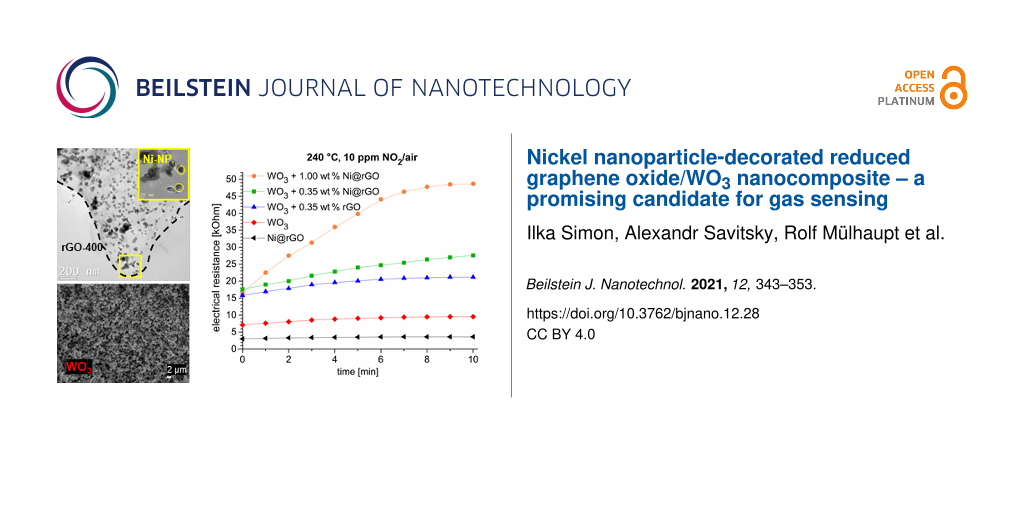
At 240 °C the electrical resistance of the 0.35 wt % Ni@rGO/WO3 sample in a gas–air environment containing 10 ppm NO2 increased 1.6-fold (from 17.6 to 27.6 kΩ, Figure 6 left).
![[2190-4286-12-28-6]](/bjnano/content/figures/2190-4286-12-28-6.png?scale=2.0&max-width=1024&background=FFFFFF)
Figure 6: Time dependence of the sensor resistance values (left) and sensor response (right) of 1.00 wt % Ni@rGO + WO3 (orange), 0.35 wt % Ni@rGO + WO3 (green), 0.35 wt % rGO + WO3 (blue), WO3 (red), and Ni@rGO (black) samples under exposure to a gas mixture containing 10 ppm NO2 in air.
Figure 6: Time dependence of the sensor resistance values (left) and sensor response (right) of 1.00 wt % Ni@...
Figure 6 (right) shows a sensor response curve for a sample that is a composite layer of Ni@rGO in the conductive polymer poly(3,4-ethylenedioxythiophene):poly(styrenesulfonate) (PEDOT:PSS). This layer is applied to a corundum substrate. In the case of NO2, the sensor response (Rgas/Rair) is, respectively, 2.9 for 1.00 wt % Ni@rGO + WO3, 1.9 for 0.35 wt % Ni@rGO + WO3, 1.6 for 0.35 wt % rGO + WO3, 1.4 for WO3, and 1.2 for Ni@rGO. Thus, the addition of Ni@rGO to WO3 enables the increase of the sensor response to NO2 and acetone vapor.
In contrast to sensors in which the sensing element consists only of rGO, sensors based on semiconductor oxide compositions, for example, WO3 with rGO, have a higher response. In the case of pure rGO, the restoration of the original parameters of the sensors may not be observed at all [8]. In addition, oxide-based composites are mechanically more durable and manufacturing sensors based on them seems to be more economically feasible due to the low content of graphene in the sensing element (up to several percent).
At present, there is no generally accepted mechanism of gas sensitivity of semiconductor oxide compositions with graphene. The reasons for the increase in the response and decrease in the operating temperature of metal oxides combined with non-oxidized graphene are synergetic effects between graphene and metal oxides as a result of chemical bonds between graphene and metal oxide. In the case of reduced graphene oxide (semiconductor), various reasons are considered, such as the appearance of p–n junctions that shift the Fermi level of the oxide. There is evidence of effective charge transfer between graphene and nanospheres through chemical bonds. Emergence of conducting channels from graphene layers is also pointed out, which increase the efficiency of charge carrier transfer in composites [8].
Based on the known literature data and the results obtained, it is possible to provide potential reasons for an enhancement of the sensitivity in the case under consideration. When Ni@rGO/WO3 sensors are exposed to NO2, with NO2, which is a strong oxidizing gas accepts electrons from WO3. As a result, NO2 transforms into NO2− on the surface of WO3. This process leads to accumulation of holes and an increase in sensor sensitivity. In addition, the rGO/WO3 contact also plays an important role in charge transfer processes and leads to the enhancement in the gas sensing performance due to the synergistic effect between rGO (p-type) WO3 (n-type) [29]. In [37,53], the formation of C–O–W bonds at the interphase boundaries was observed, when studying a rGO/WO3 composite using XPS and Raman spectroscopy. Such bonds can play an important role also in our case with regard to charge transfer. It has been established that adsorption of NO2 molecules will cause upward band bending by capturing free electrons from the conduction band and shift the Fermi level of WO3 away from the conduction band toward the valence band. Processes on the WO3 surface make it possible for the work function of WO3 to lower to a point close to that of rGO [37]. The latter facilitates transfer of electrons at the rGO/WO3 interface. The continuous capture of electrons by chemisorption of NO2 gases at the surface of WO3 facilitates the charge transfer from rGO to WO3. At the expense of C–O–W bonds, hole transfer from WO3 to rGO will occur. Thus, it has been shown that C–O–W bonds are responsible for enhancing the charge carrier transfer rate [54]. In addition, graphene sheets in the composite create a hierarchical nanostructure and facilitate the diffusion of NO2 molecules, increasing the contacts and enhancing the chemisorption of the gas. rGO has large specific area and more active sites.
Gas sensors of n-type semiconductors based on oxides exhibit resistance changes induced by chemisorption of oxygen adions (O− and O2−) that interact with reducing gases [55,56] such as acetone. A free electron appears in the conduction band of the semiconductor after the interaction of the chemisorbed oxygen adions and the target gas [57]. When acetone adsorbs on the surface of such a sensor material, preadsorbed oxygen adions are released according to the reaction [58]:
![[Graphic 1]](/bjnano/content/inline/2190-4286-12-28-i1.svg?max-width=637&scale=1.18182)
The same is true for CO [57]:
![[Graphic 2]](/bjnano/content/inline/2190-4286-12-28-i2.svg?max-width=637&scale=1.18182)
As a result, electrons that were trapped in the oxygen adions return back to the conduction band of WO3. Thus, the resistance of WO3 decreases upon exposure to these gases. An increase in the sensitivity to acetone of the entire composition 0.35 wt % Ni@rGO/WO3 may be associated with further electronic interaction between WO3 particles (n-type) and Ni@rGO (p-type). In this case, the transfer of electrons from WO3 to rGO leads to the formation of spatially separated regions of positive and negative charges (possibly, a p–n junction is formed). It was shown [59] that electrons that were transferred from the n-type semiconductor and stored in the rGO sheets are withdrawn upon exposure to gas, thereby restoring the hole concentration and p-type conductivity of rGO. This is made possible by the energy band alignment between the semiconductor and rGO, the electron acceptor functionalization of the analyzed gas, and the p-type conductivity of the rGO. Thus, the electron-depleted WO3 surface is more sensitive to the adsorption of acetone molecules and the transition of electrons from the adsorbed gas to the WO3 conduction band.
When considering the possible mechanism of the influence of nickel on the sensory properties of the Ni/rGO/WO3 composite, in addition to selective catalytic activity, it is also possible to refer to the existing explanation for the interaction of clusters of metal particles with a semiconductor. In accordance with the literature data, the role of nickel in increasing the sensory sensitivity is most likely associated with the spillover effect [60,61]. When interacting with a gas atom, the barrier height at the Ni/rGO interface decreases due to this effect (the possibility of electron transfer from nickel particles to rGO and WO3), which leads to a greater decrease in the resistance of the composite. In our case, these processes enhance the diffusion of charges at the WO3/rGO interface, but the role of nickel particles remains to be further clarified.
Magnetic measurements
In order to investigate if nickel oxidation had occurred in the Ni@rGO composite during the heat treatment in the study of sensory properties (250 °C), the following model experiment was performed. The original Ni@rGO composite was annealed at a temperature of 250 °C for 2 h. In the following, its magnetic properties, namely the Curie temperature was determined from the temperature dependences of magnetization and magnetic susceptibility.
The results of the magnetic analysis (Figure 7a) indicate that the magnetic phase in the Ni@rGO composite is pure nickel. The Curie temperature of the composite (Tc = 630 K, Figure 7, left) and the reference value for pure nickel [62] coincide (Figure S3, Supporting Information File 1). Moreover, the fraction of the magnetic phase in the Ni@rGO composite, as shown by magnetization measurements, is 7.8 wt %. The same amount of nickel is present in the original Ni@rGO composite without heat treatment.
![[2190-4286-12-28-7]](/bjnano/content/figures/2190-4286-12-28-7.png?scale=2.0&max-width=1024&background=FFFFFF)
Figure 7: Left: magnetization as a function of temperature for the Ni@rGO composite in argon atmosphere. Right: magnetic susceptibility as a function of temperature for nickel in argon atmosphere.
Figure 7: Left: magnetization as a function of temperature for the Ni@rGO composite in argon atmosphere. Righ...
The temperature dependence of the magnetization was determined during several heating–cooling cycles. It was noted that with an increase in the number of cycles, the Сurie temperature of the sample increased from 345 to 357 °C. Most likely, the increase in the Curie temperature is associated with an increase in the size of the nickel particles as a result of their sintering in agglomerates with an increase in the degree of crystallinity. The maximum temperature during cycling reached 450 °C. It can also be assumed that a sintering of nickel nanoparticles (approximately 25 nm in size), which are located in the partly formed agglomerates in the initial composite, is possible (Figure 2, right).
The increase in the Curie temperature with the size of nanoparticles is known [63,64]. It is explained by a decrease in the fraction of the nickel particle surface layer with a noncollinear spin configuration, which causes the formation of a surface spin canting due to thermal fluctuation of magnetic moments. Figure 7 shows the temperature dependence of the magnetization obtained in the course of the last measurement cycle at which, for nickel particles, ferromagnetic rather than superparamagnetic behavior is manifested. Hence, the results of measurements of the magnetic susceptibility and magnetization indicate the presence of only a metallic nickel phase in the Ni@rGO composite after heat treatment in air.
Сonclusion
Ni@rGO nanocomposites were found to be promising materials that enable the preparation of WO3 gas and vapor sensor elements with improved sensory response. The addition of a very small amount of Ni@rGO (0.35 wt %) to WO3 increases the gas response regarding NO2 traces in air significantly compared to the WO3 element without the addition of metal and graphene oxide. Low concentrations of acetone (3500 ppm) were better detected by the Ni@rGO/WO3 composite than the higher concentration of 35,000 ppm. For CO gas, the response time and the recovery time were Tres ≈ 7 min and Trec ≈ 2 min, respectively. The facile preparation of nickel nanoparticles supported on reduced graphene oxide paves the way for their application as dopant in other metal oxide gas sensors.
Experimental
Due to the sensitivity of the precursor substances towards moisture and oxidation, all experiments were carried out in a purified argon (grade 99.998 vol %) or nitrogen (grade 99.996 vol %) atmosphere by using standard Schlenk techniques. Samples were prepared and stored in a MBraun Glovebox. Solvents (acetonitrile, n-hexane, and methylene chloride) were dried by using a MBraun solvent purification system or distilled (1-methylimidazole and 1-chlorobutane) and stored over 4 Å molecular sieves in a nitrogen atmosphere. Final water contents measured by coulometric Karl Fischer titration (ECH/ANALYTIK JENA AQUA 40.00) did not exceed 10 ppm.
Bis(1,5-cyclooctadiene)nickel(0) (Ni(COD)2) was purchased from ABCR, stored at −4 °C and used without further purification. The ionic liquid [BMIm][NTf2] was synthesized according to literature by reacting 1-methylimidazole with 1-chlorobutane to yield first [BMIm][Cl], which was further reacted with LiNTf2 to give [BMIm][NTf2] [65,66]. The IL was dried in a turbo molecular pump vacuum (10−7 mbar) at 80 °C for three days. Characterization was carried out by 1H and 13C NMR. Quantitative anion exchange and IL purity of 99.9% was assessed by ion chromatography (Dionex ICS-1100, with IonPac® AS22, 4 × 250 mm column). The water content, measured by coulometric Karl Fischer titration, was below 10 ppm. rGO was synthesized in a two-step oxidation and thermal reduction process using natural graphite (type KFL 99.5 from AMG Mining AG, former Kropfmühl AG, Passau, Germany) as starting material. Graphite was oxidized according to [67]. Reduction of the graphite oxide was performed at 400 °C. Before using rGO in the nanoparticle synthesis, it was dried at 100 °C using a turbo molecular pump at 5 × 10⁻⁷ mbar for several days.
Preparation of Ni@rGO in ionic liquid
Nickel nanoparticles on rGO (Ni@rGO) were prepared in septum-sealed 10 mL microwave vessels (CEM GmbH, Germany) in a CEM Discover microwave under argon atmosphere. Ni(COD)2 (49.2 mg, 0.178 mmol) and rGO (10 mg) were suspended for 2 h in the dried and deoxygenated IL (2 g [BMIm][NTf2]) before microwave decomposition (230 °C, 10 min, 50 W) to obtain a dispersion of 0.5 wt % of Ni nanoparticles on rGO in ionic liquid.
Preparation of WO3 nanopowder
Tungsten oxide nanopowder was prepared according to [52] using the sol–gel method. A 1.23 mol/L aqueous solution of sodium tungstate dihydrate (Na2WO3⋅2H2O) was added into a 12 mol/L aqueous solution of nitric acid under constant rapid stirring. The prepared sol of tungstic acid was washed in distilled water using multiple centrifugation steps. After drying until the xerogel was formed, the WO3 nanopowder was calcined at 600 °C for 2 h.
Ni@rGO mixing of WO3 xerogel
The Ni@rGO admixing of WO3 samples was done by preparing a physical mixture of the WO3 xerogel and Ni@rGO. At a pressure of 150 kPa, tablets were pressed from the powder (diameter 10 mm, thickness 2.5 mm, weight 0.75 g), which were sintered in air at 450 °C (4 h).
Characterization
Powder X-ray diffraction, P-XRD data were measured at ambient temperature on a Bruker D2 Phaser using a flat sample holder and Cu Kα radiation (λ = 1.54182 Å, 35 kV). Samples had been precipitated with acetonitrile from the nanoparticle/ionic liquid dispersion and washed several times with acetonitrile. P-XRD patterns were recorded for 1 h (2θ = 5–100°).
Atomic absorption spectroscopy, AAS for metal analysis was performed on a PerkinElmer PinAAcle 900T, equipped with a flame furnace. Flame-AAS with an air/acetylene flame was used for the determination of the nickel content. Samples were digested in hot aqua regia two times (30 mL). The residues were re-dissolved in aqua regia, filtered and brought with water to a total volume of 10 mL. For the nickel measurements the samples were diluted 1:100.
Transmission electron microscopy, TEM was performed with a FEI Tecnai G2 F20 electron microscope [68] operated at 200 kV accelerating voltage or FEI Titan 80-300 TEM operated at 300 kV accelerating voltage [69]. Conventional TEM images were recorded with a Gatan UltraScan 1000P detector. TEM samples were prepared by drop casting the with acetonitrile diluted material on 200 µm carbon-coated copper grids, followed by washing the grid several times with acetonitrile to remove the excess ionic liquid. The size distribution was determined manually or with the aid of the Gatan Digital Micrograph software from at least 50 individual particles.
Gas sensing properties of the sensor elements were characterized using a custom-designed flow-type sensing measurement system inside a corundum chamber with precisely controlled temperature and atmosphere. Calibrated according to STB ISO 9001-2009, a CO/N2 mixture was received from Joint Stock Company "Kryon”. Liquid acetone was classified as “chemically pure” (purissimum). The NO2 gas was obtained by dissolving Cu in nitric acid (“chemically pure” grade). The CO/air mixture was measured in flow mode. NO2 and acetone were measured in a static mode. Here, a given amount of gas was introduced into a sealed chamber with a volume of 120 cm3. Electrical resistance of samples WO3, rGO/WO3, 0.35 wt % Ni@rGO/WO3 in the range of 20–240 °С was measured by the two-probe method in a corundum cell using an Agilent 34401 digital multimeter. The cell was placed in a tube furnace with a temperature regulator. To enhance electrical conductivity and to improve contact Ag electrodes were deposited on parallel sides of the pellets. The measurement procedure was carried out for NO2 and acetone in a stationary regime in a precisely controlled atmosphere (10 ppm NO2 and 3500 ppm acetone in air) according to the method proposed in [70]. The sensing element was placed into a preheated and thermostabilized chamber. Then, calibrated testing gas mixtures were injected into the chamber and measurements were carried out at the indicated temperature. Sensitivity to CO was measured in a dynamic regime using the CO/N2 gas mixture in flow mode. The CO/N2 mixture was fed at a rate of 2 L/h for aperiod of 10 min.
We note that it was not possible to set a repeated exposure to analyte gas and Trec in a stationary mode for technical reasons. In the stationary regime, the flanges of the measuring cell have rubber plugs through which the required amount of analyte is injected from a microdispenser with a needle. To determine parameters such as Trec and Tres in this stationary regime the operation of purging the cell with air would be necessary. For this, the cell flanges need to be replaced with other flanges. The temperature at which the measurements were carried out in the stationary mode excludes quick manipulations of these flanges. Even at room temperature, it takes 1 to 2 min to partially disassemble the chamber and replace the flanges with plugs with flanges with air purge pipes. Therefore, it was practically impossible to measure the relaxation time in a heated cell. Even at room temperature, at best, the measurement procedure will be incorrect, since the possible recovery time is comparable to the time of manipulations with the cell components.
Magnetic measurements were carried out by using the ponderomotive method with automatized installation for measuring magnetic characteristics and for the determination of magnetic impurities in substances by nondestructive testing with a precision to 0.01%. The measurement error for the specific magnetization of the measured samples is equal to ±0.005 A·m2/kg, for the magnetic susceptibility of samples with known mass it is equal to ±1 × 10–11 m3/kg.
Supporting Information
| Supporting Information File 1: Comparison with other gas sensors as well as the sensor response figures for CO and acetone. | ||
| Format: PDF | Size: 429.1 KB | Download |
Acknowledgements
We thank Dr. Juri Barthel from the Ernst Ruska-Centre (Forschungszentrum Jülich GmbH, Jülich, Germany) for technical support.
Funding
Authors are thankful to the Deutsche Forschungsgemeinschaft (DFG) for financial support within the priority project SPP 1708 “Material Synthesis Near Room Temperature” through grant Ja466/31-1, Ja466/31-2. We thank the Ernst Ruska-Centre (Forschungszentrum Jülich GmbH, Jülich, Germany) for access to the TEM facility under project number ER-C D-066 and in the core-facilities program through grant MA 1280/40-1. We are thankful to the Belarusian Republican Foundation for Fundamental Research for financial support (BRFFR).
References
-
Mane, A. T.; Kulkarni, S. B.; Navale, S. T.; Ghanwat, A. A.; Shinde, N. M.; Kim, J.; Patil, V. B. Ceram. Int. 2014, 40, 16495–16502. doi:10.1016/j.ceramint.2014.08.001
Return to citation in text: [1] -
Tian, W.; Liu, X.; Yu, W. Appl. Sci. 2018, 8, 1118–1138. doi:10.3390/app8071118
Return to citation in text: [1] -
Meng, F.-L.; Guo, Z.; Huang, X.-J. TrAC, Trends Anal. Chem. 2015, 68, 37–47. doi:10.1016/j.trac.2015.02.008
Return to citation in text: [1] -
Varghese, S. S.; Lonkar, S.; Singh, K. K.; Swaminathan, S.; Abdala, A. Sens. Actuators, B 2015, 218, 160–183. doi:10.1016/j.snb.2015.04.062
Return to citation in text: [1] [2] -
Basu, S.; Bhattacharyya, P. Sens. Actuators, B 2012, 173, 1–21. doi:10.1016/j.snb.2012.07.092
Return to citation in text: [1] -
Nunes, D.; Pimentel, A.; Gonçalves, A.; Pereira, S.; Branquinho, R.; Barquinha, P.; Fortunato, E.; Martins, R. Semicond. Sci. Technol. 2019, 34, 043001. doi:10.1088/1361-6641/ab011e
Return to citation in text: [1] [2] [3] -
Wetchakun, K.; Samerjai, T.; Tamaekong, N.; Liewhiran, C.; Siriwong, C.; Kruefu, V.; Wisitsoraat, A.; Tuantranont, A.; Phanichphant, S. Sens. Actuators, B 2011, 160, 580–591. doi:10.1016/j.snb.2011.08.032
Return to citation in text: [1] [2] -
Sun, D.; Luo, Y.; Debliquy, M.; Zhang, C. Beilstein J. Nanotechnol. 2018, 9, 2832–2844. doi:10.3762/bjnano.9.264
Return to citation in text: [1] [2] [3] [4] [5] -
Jeevitha, G.; Abhinayaa, R.; Mangalaraj, D.; Ponpandian, N.; Meena, P.; Mounasamy, V.; Madanagurusamy, S. Nanoscale Adv. 2019, 1, 1799–1811. doi:10.1039/c9na00048h
Return to citation in text: [1] -
Long, H.; Zeng, W.; Zhang, H. J. Mater. Sci.: Mater. Electron. 2015, 26, 4698–4707. doi:10.1007/s10854-015-2896-4
Return to citation in text: [1] -
Xia, Y.; Li, R.; Chen, R.; Wang, J.; Xiang, L. Sensors 2018, 18, 1456–1477. doi:10.3390/s18051456
Return to citation in text: [1] -
Mattinen, M.; Wree, J.-L.; Stegmann, N.; Ciftyurek, E.; Achhab, M. E.; King, P. J.; Mizohata, K.; Räisänen, J.; Schierbaum, K. D.; Devi, A.; Ritala, M.; Leskelä, M. Chem. Mater. 2018, 30, 8690–8701. doi:10.1021/acs.chemmater.8b04129
Return to citation in text: [1] -
D’Anna, F.; Grilli, M. L.; Petrucci, R.; Feroci, M. Metals (Basel, Switz.) 2020, 10, 475. doi:10.3390/met10040475
Return to citation in text: [1] -
Kukkola, J.; Mäklin, J.; Halonen, N.; Kyllönen, T.; Tóth, G.; Szabó, M.; Shchukarev, A.; Mikkola, J.-P.; Jantunen, H.; Kordás, K. Sens. Actuators, B 2011, 153, 293–300. doi:10.1016/j.snb.2010.10.043
Return to citation in text: [1] -
Vasilopoulou, M.; Palilis, L. C.; Georgiadou, D. G.; Douvas, A. M.; Argitis, P.; Kennou, S.; Sygellou, L.; Papadimitropoulos, G.; Kostis, I.; Stathopoulos, N. A.; Davazoglou, D. Adv. Funct. Mater. 2011, 21, 1489–1497. doi:10.1002/adfm.201002171
Return to citation in text: [1] [2] -
Li, J.; Liu, X.; Cui, J.; Sun, J. ACS Appl. Mater. Interfaces 2015, 7, 10108–10114. doi:10.1021/am508121p
Return to citation in text: [1] -
Gillet, M.; Aguir, K.; Lemire, C.; Gillet, E.; Schierbaum, K. Thin Solid Films 2004, 467, 239–246. doi:10.1016/j.tsf.2004.04.018
Return to citation in text: [1] -
Gu, H.; Wang, Z.; Hu, Y. Sensors 2012, 12, 5517–5550. doi:10.3390/s120505517
Return to citation in text: [1] [2] -
Esfandiar, A.; Irajizad, A.; Akhavan, O.; Ghasemi, S.; Gholami, M. R. Int. J. Hydrogen Energy 2014, 39, 8169–8179. doi:10.1016/j.ijhydene.2014.03.117
Return to citation in text: [1] [2] -
Ramkumar, S.; Rajarajan, G. Appl. Phys. A: Mater. Sci. Process. 2017, 123, 401. doi:10.1007/s00339-017-0983-5
Return to citation in text: [1] -
Van Tong, P.; Hoa, N. D.; Van Duy, N.; Le, D. T. T.; Van Hieu, N. Sens. Actuators, B 2016, 223, 453–460. doi:10.1016/j.snb.2015.09.108
Return to citation in text: [1] -
Ji, H.; Zeng, W.; Li, Y. Nanoscale 2019, 11, 22664–22684. doi:10.1039/c9nr07699a
Return to citation in text: [1] -
Eranna, G.; Joshi, B. C.; Runthala, D. P.; Gupta, R. P. Crit. Rev. Solid State Mater. Sci. 2004, 29, 111–188. doi:10.1080/10408430490888977
Return to citation in text: [1] -
Woo, H.-S.; Kwak, C.-H.; Chung, J.-H.; Lee, J.-H. Sens. Actuators, B 2015, 216, 358–366. doi:10.1016/j.snb.2015.04.035
Return to citation in text: [1] -
Xiao, X.; Zhou, X.; Ma, J.; Zhu, Y.; Cheng, X.; Luo, W.; Deng, Y. ACS Appl. Mater. Interfaces 2019, 11, 26268–26276. doi:10.1021/acsami.9b08128
Return to citation in text: [1] -
Wang, T.; Huang, D.; Yang, Z.; Xu, S.; He, G.; Li, X.; Hu, N.; Yin, G.; He, D.; Zhang, L. Nano-Micro Lett. 2016, 8, 95–119. doi:10.1007/s40820-015-0073-1
Return to citation in text: [1] [2] -
Mao, S.; Lu, G.; Yu, K.; Bo, Z.; Chen, J. Adv. Mater. (Weinheim, Ger.) 2010, 22, 3521–3526. doi:10.1002/adma.201000520
Return to citation in text: [1] -
Li, Q.; Liu, W.; Cao, G.; Li, X.; Wang, X. Appl. Phys. Lett. 2016, 108, 221604–221607. doi:10.1063/1.4952619
Return to citation in text: [1] -
Su, P.-G.; Peng, S.-L. Talanta 2015, 132, 398–405. doi:10.1016/j.talanta.2014.09.034
Return to citation in text: [1] [2] -
Yin, P. T.; Shah, S.; Chhowalla, M.; Lee, K.-B. Chem. Rev. 2015, 115, 2483–2531. doi:10.1021/cr500537t
Return to citation in text: [1] -
Mirzaei, A.; Kim, S. S.; Kim, H. W. J. Hazard. Mater. 2018, 357, 314–331. doi:10.1016/j.jhazmat.2018.06.015
Return to citation in text: [1] -
Zhang, J.; Zeng, D.; Wang, H.; Qin, Z.; Pang, A.; Xie, C. Mater. Lett. 2017, 204, 27–30. doi:10.1016/j.matlet.2017.06.008
Return to citation in text: [1] -
Mahajan, S.; Jagtap, S. Appl. Mater. Today 2020, 18, 100483–100512. doi:10.1016/j.apmt.2019.100483
Return to citation in text: [1] -
Bhati, V. S.; Ranwa, S.; Rajamani, S.; Kumari, K.; Raliya, R.; Biswas, P.; Kumar, M. ACS Appl. Mater. Interfaces 2018, 10, 11116–11124. doi:10.1021/acsami.7b17877
Return to citation in text: [1] [2] -
Wang, T.; Hao, J.; Zheng, S.; Sun, Q.; Zhang, D.; Wang, Y. Nano Res. 2018, 11, 791–803. doi:10.1007/s12274-017-1688-y
Return to citation in text: [1] -
Le Hoa, T.; Tien, H. N.; van Luan, H.; Chung, J. S.; Hur, S. H. Sens. Actuators, B 2013, 185, 701–705. doi:10.1016/j.snb.2013.05.050
Return to citation in text: [1] -
Jie, X.; Zeng, D.; Zhang, J.; Xu, K.; Wu, J.; Zhu, B.; Xie, C. Sens. Actuators, B 2015, 220, 201–209. doi:10.1016/j.snb.2015.05.047
Return to citation in text: [1] [2] [3] -
Zhang, J.; Wu, J.; Wang, X.; Zeng, D.; Xie, C. Sens. Actuators, B 2017, 243, 1010–1019. doi:10.1016/j.snb.2016.12.062
Return to citation in text: [1] -
Piloto, C.; Shafiei, M.; Khan, H.; Gupta, B.; Tesfamichael, T.; Motta, N. Appl. Surf. Sci. 2018, 434, 126–133. doi:10.1016/j.apsusc.2017.10.152
Return to citation in text: [1] -
Singkammo, S.; Wisitsoraat, A.; Sriprachuabwong, C.; Tuantranont, A.; Phanichphant, S.; Liewhiran, C. ACS Appl. Mater. Interfaces 2015, 7, 3077–3092. doi:10.1021/acsami.5b00161
Return to citation in text: [1] -
Ghosal, S.; Bhattacharyya, P. CSI Trans. ICT 2020, 8, 117–122. doi:10.1007/s40012-020-00299-z
Return to citation in text: [1] -
Chen, L.; Huang, L.; Lin, Y.; Sai, L.; Chang, Q.; Shi, W.; Chen, Q. Sens. Actuators, B 2018, 255, 1482–1490. doi:10.1016/j.snb.2017.08.158
Return to citation in text: [1] -
Wang, Z.; Zhang, Y.; Liu, S.; Zhang, T. Sens. Actuators, B 2016, 222, 893–903. doi:10.1016/j.snb.2015.09.027
Return to citation in text: [1] -
Davar, F.; Fereshteh, Z.; Salavati-Niasari, M. J. Alloys Compd. 2009, 476, 797–801. doi:10.1016/j.jallcom.2008.09.121
Return to citation in text: [1] -
LaGrow, A. P.; Ingham, B.; Toney, M. F.; Tilley, R. D. J. Phys. Chem. C 2013, 117, 16709–16718. doi:10.1021/jp405314g
Return to citation in text: [1] -
Wegner, S.; Rutz, C.; Schütte, K.; Barthel, J.; Bushmelev, A.; Schmidt, A.; Dilchert, K.; Fischer, R. A.; Janiak, C. Chem. – Eur. J. 2017, 23, 6330–6340. doi:10.1002/chem.201605251
Return to citation in text: [1] [2] -
Chaban, V. V.; Fileti, E. E. RSC Adv. 2015, 5, 81229–81234. doi:10.1039/c5ra16857k
Return to citation in text: [1] -
Marquardt, D.; Vollmer, C.; Thomann, R.; Steurer, P.; Mülhaupt, R.; Redel, E.; Janiak, C. Carbon 2011, 49, 1326–1332. doi:10.1016/j.carbon.2010.09.066
Return to citation in text: [1] -
Schmitz, A.; Schütte, K.; Ilievski, V.; Barthel, J.; Burk, L.; Mülhaupt, R.; Yue, J.; Smarsly, B.; Janiak, C. Beilstein J. Nanotechnol. 2017, 8, 2474–2483. doi:10.3762/bjnano.8.247
Return to citation in text: [1] [2] -
Srivastava, S.; Jain, K.; Singh, V. N.; Singh, S.; Vijayan, N.; Dilawar, N.; Gupta, G.; Senguttuvan, T. D. Nanotechnology 2012, 23, 205501. doi:10.1088/0957-4484/23/20/205501
Return to citation in text: [1] -
Qu, W.; Bao, H.; Zhang, L.; Chen, G. Chem. – Eur. J. 2012, 18, 15746–15752. doi:10.1002/chem.201202913
Return to citation in text: [1] -
Haiduk, Y. S.; Khort, A. A.; Lapchuk, N. M.; Savitsky, A. A. J. Solid State Chem. 2019, 273, 25–31. doi:10.1016/j.jssc.2019.02.023
Return to citation in text: [1] [2] -
Akhavan, O.; Choobtashani, M.; Ghaderi, E. J. Phys. Chem. C 2012, 116, 9653–9659. doi:10.1021/jp301707m
Return to citation in text: [1] -
Guo, J.; Li, Y.; Zhu, S.; Chen, Z.; Liu, Q.; Zhang, D.; Moon, W.-J.; Song, D.-M. RSC Adv. 2012, 2, 1356–1363. doi:10.1039/c1ra00621e
Return to citation in text: [1] -
Morrison, S. R. Sens. Actuators 1987, 12, 425–440. doi:10.1016/0250-6874(87)80061-6
Return to citation in text: [1] -
Heiland, G. Sens. Actuators 1981, 2, 343–361. doi:10.1016/0250-6874(81)80055-8
Return to citation in text: [1] -
Kumar, A.; Kumar, R.; Singh, R.; Prasad, B.; Kumar, D.; Kumar, M. Arabian J. Sci. Eng. 2021, 46, 617–630. doi:10.1007/s13369-020-04630-3
Return to citation in text: [1] [2] -
Qin, L.; Xu, J.; Dong, X.; Pan, Q.; Cheng, Z.; Xiang, Q.; Li, F. Nanotechnology 2008, 19, 185705. doi:10.1088/0957-4484/19/18/185705
Return to citation in text: [1] -
Choi, S.-J.; Jang, B.-H.; Lee, S.-J.; Min, B. K.; Rothschild, A.; Kim, I.-D. ACS Appl. Mater. Interfaces 2014, 6, 2588–2597. doi:10.1021/am405088q
Return to citation in text: [1] -
Sholehah, A.; Faroz, D. F.; Huda, N.; Utari, L.; Septiani, N. L. W.; Yuliarto, B. Chemosensors 2019, 8, 2. doi:10.3390/chemosensors8010002
Return to citation in text: [1] -
Hübner, M.; Koziej, D.; Grunwaldt, J.-D.; Weimar, U.; Barsan, N. Phys. Chem. Chem. Phys. 2012, 14, 13249–13254. doi:10.1039/c2cp41349c
Return to citation in text: [1] -
Ashcroft, N. W.; Mermin, N. D. Solid state physics (Repr); Brooks/Cole Thomson Learning: South Melbourne, 2012.
Return to citation in text: [1] -
He, X.; Zhong, W.; Au, C.-T.; Du, Y. Nanoscale Res. Lett. 2013, 8, 446. doi:10.1186/1556-276x-8-446
Return to citation in text: [1] -
Cao, L.-f.; Xie, D.; Guo, M.-x.; Park, H. S.; Fujita, T. Trans. Nonferrous Met. Soc. China 2007, 17, 1451–1455. doi:10.1016/s1003-6326(07)60293-3
Return to citation in text: [1] -
Bonhôte, P.; Dias, A.-P.; Papageorgiou, N.; Kalyanasundaram, K.; Grätzel, M. Inorg. Chem. 1996, 35, 1168–1178. doi:10.1021/ic951325x
Return to citation in text: [1] -
Burrell, A. K.; Sesto, R. E. D.; Baker, S. N.; McCleskey, T. M.; Baker, G. A. Green Chem. 2007, 9, 449–454. doi:10.1039/b615950h
Return to citation in text: [1] -
Hummers, W. S., Jr.; Offeman, R. E. J. Am. Chem. Soc. 1958, 80, 1339. doi:10.1021/ja01539a017
Return to citation in text: [1] -
Luysberg, M.; Heggen, M.; Tillmann, K. J. Large-Scale Res. Facil. 2016, 2, A77. doi:10.17815/jlsrf-2-138
Return to citation in text: [1] -
Thust, A.; Barthel, J.; Tillmann, K. J. Large-Scale Res. Facil. 2016, 2, A41. doi:10.17815/jlsrf-2-66
Return to citation in text: [1] -
Krechmar, S.; Bezpalchenko, V.; Mishekin, A. Zavod. Lab., Diagn. Mater. 2008, 75, 21–22.
Return to citation in text: [1]
| 30. | Yin, P. T.; Shah, S.; Chhowalla, M.; Lee, K.-B. Chem. Rev. 2015, 115, 2483–2531. doi:10.1021/cr500537t |
| 31. | Mirzaei, A.; Kim, S. S.; Kim, H. W. J. Hazard. Mater. 2018, 357, 314–331. doi:10.1016/j.jhazmat.2018.06.015 |
| 69. | Thust, A.; Barthel, J.; Tillmann, K. J. Large-Scale Res. Facil. 2016, 2, A41. doi:10.17815/jlsrf-2-66 |
| 32. | Zhang, J.; Zeng, D.; Wang, H.; Qin, Z.; Pang, A.; Xie, C. Mater. Lett. 2017, 204, 27–30. doi:10.1016/j.matlet.2017.06.008 |
| 70. | Krechmar, S.; Bezpalchenko, V.; Mishekin, A. Zavod. Lab., Diagn. Mater. 2008, 75, 21–22. |
| 52. | Haiduk, Y. S.; Khort, A. A.; Lapchuk, N. M.; Savitsky, A. A. J. Solid State Chem. 2019, 273, 25–31. doi:10.1016/j.jssc.2019.02.023 |
| 68. | Luysberg, M.; Heggen, M.; Tillmann, K. J. Large-Scale Res. Facil. 2016, 2, A77. doi:10.17815/jlsrf-2-138 |
| 67. | Hummers, W. S., Jr.; Offeman, R. E. J. Am. Chem. Soc. 1958, 80, 1339. doi:10.1021/ja01539a017 |
| 39. | Piloto, C.; Shafiei, M.; Khan, H.; Gupta, B.; Tesfamichael, T.; Motta, N. Appl. Surf. Sci. 2018, 434, 126–133. doi:10.1016/j.apsusc.2017.10.152 |
| 40. | Singkammo, S.; Wisitsoraat, A.; Sriprachuabwong, C.; Tuantranont, A.; Phanichphant, S.; Liewhiran, C. ACS Appl. Mater. Interfaces 2015, 7, 3077–3092. doi:10.1021/acsami.5b00161 |
| 8. | Sun, D.; Luo, Y.; Debliquy, M.; Zhang, C. Beilstein J. Nanotechnol. 2018, 9, 2832–2844. doi:10.3762/bjnano.9.264 |
| 38. | Zhang, J.; Wu, J.; Wang, X.; Zeng, D.; Xie, C. Sens. Actuators, B 2017, 243, 1010–1019. doi:10.1016/j.snb.2016.12.062 |
| 36. | Le Hoa, T.; Tien, H. N.; van Luan, H.; Chung, J. S.; Hur, S. H. Sens. Actuators, B 2013, 185, 701–705. doi:10.1016/j.snb.2013.05.050 |
| 37. | Jie, X.; Zeng, D.; Zhang, J.; Xu, K.; Wu, J.; Zhu, B.; Xie, C. Sens. Actuators, B 2015, 220, 201–209. doi:10.1016/j.snb.2015.05.047 |
| 33. | Mahajan, S.; Jagtap, S. Appl. Mater. Today 2020, 18, 100483–100512. doi:10.1016/j.apmt.2019.100483 |
| 34. | Bhati, V. S.; Ranwa, S.; Rajamani, S.; Kumari, K.; Raliya, R.; Biswas, P.; Kumar, M. ACS Appl. Mater. Interfaces 2018, 10, 11116–11124. doi:10.1021/acsami.7b17877 |
| 35. | Wang, T.; Hao, J.; Zheng, S.; Sun, Q.; Zhang, D.; Wang, Y. Nano Res. 2018, 11, 791–803. doi:10.1007/s12274-017-1688-y |
| 34. | Bhati, V. S.; Ranwa, S.; Rajamani, S.; Kumari, K.; Raliya, R.; Biswas, P.; Kumar, M. ACS Appl. Mater. Interfaces 2018, 10, 11116–11124. doi:10.1021/acsami.7b17877 |
| 15. | Vasilopoulou, M.; Palilis, L. C.; Georgiadou, D. G.; Douvas, A. M.; Argitis, P.; Kennou, S.; Sygellou, L.; Papadimitropoulos, G.; Kostis, I.; Stathopoulos, N. A.; Davazoglou, D. Adv. Funct. Mater. 2011, 21, 1489–1497. doi:10.1002/adfm.201002171 |
| 41. | Ghosal, S.; Bhattacharyya, P. CSI Trans. ICT 2020, 8, 117–122. doi:10.1007/s40012-020-00299-z |
| 19. | Esfandiar, A.; Irajizad, A.; Akhavan, O.; Ghasemi, S.; Gholami, M. R. Int. J. Hydrogen Energy 2014, 39, 8169–8179. doi:10.1016/j.ijhydene.2014.03.117 |
| 48. | Marquardt, D.; Vollmer, C.; Thomann, R.; Steurer, P.; Mülhaupt, R.; Redel, E.; Janiak, C. Carbon 2011, 49, 1326–1332. doi:10.1016/j.carbon.2010.09.066 |
| 49. | Schmitz, A.; Schütte, K.; Ilievski, V.; Barthel, J.; Burk, L.; Mülhaupt, R.; Yue, J.; Smarsly, B.; Janiak, C. Beilstein J. Nanotechnol. 2017, 8, 2474–2483. doi:10.3762/bjnano.8.247 |
| 50. | Srivastava, S.; Jain, K.; Singh, V. N.; Singh, S.; Vijayan, N.; Dilawar, N.; Gupta, G.; Senguttuvan, T. D. Nanotechnology 2012, 23, 205501. doi:10.1088/0957-4484/23/20/205501 |
| 46. | Wegner, S.; Rutz, C.; Schütte, K.; Barthel, J.; Bushmelev, A.; Schmidt, A.; Dilchert, K.; Fischer, R. A.; Janiak, C. Chem. – Eur. J. 2017, 23, 6330–6340. doi:10.1002/chem.201605251 |
| 47. | Chaban, V. V.; Fileti, E. E. RSC Adv. 2015, 5, 81229–81234. doi:10.1039/c5ra16857k |
| 44. | Davar, F.; Fereshteh, Z.; Salavati-Niasari, M. J. Alloys Compd. 2009, 476, 797–801. doi:10.1016/j.jallcom.2008.09.121 |
| 45. | LaGrow, A. P.; Ingham, B.; Toney, M. F.; Tilley, R. D. J. Phys. Chem. C 2013, 117, 16709–16718. doi:10.1021/jp405314g |
| 42. | Chen, L.; Huang, L.; Lin, Y.; Sai, L.; Chang, Q.; Shi, W.; Chen, Q. Sens. Actuators, B 2018, 255, 1482–1490. doi:10.1016/j.snb.2017.08.158 |
| 43. | Wang, Z.; Zhang, Y.; Liu, S.; Zhang, T. Sens. Actuators, B 2016, 222, 893–903. doi:10.1016/j.snb.2015.09.027 |
| 51. | Qu, W.; Bao, H.; Zhang, L.; Chen, G. Chem. – Eur. J. 2012, 18, 15746–15752. doi:10.1002/chem.201202913 |
| 49. | Schmitz, A.; Schütte, K.; Ilievski, V.; Barthel, J.; Burk, L.; Mülhaupt, R.; Yue, J.; Smarsly, B.; Janiak, C. Beilstein J. Nanotechnol. 2017, 8, 2474–2483. doi:10.3762/bjnano.8.247 |
| 46. | Wegner, S.; Rutz, C.; Schütte, K.; Barthel, J.; Bushmelev, A.; Schmidt, A.; Dilchert, K.; Fischer, R. A.; Janiak, C. Chem. – Eur. J. 2017, 23, 6330–6340. doi:10.1002/chem.201605251 |
| 1. | Mane, A. T.; Kulkarni, S. B.; Navale, S. T.; Ghanwat, A. A.; Shinde, N. M.; Kim, J.; Patil, V. B. Ceram. Int. 2014, 40, 16495–16502. doi:10.1016/j.ceramint.2014.08.001 |
| 5. | Basu, S.; Bhattacharyya, P. Sens. Actuators, B 2012, 173, 1–21. doi:10.1016/j.snb.2012.07.092 |
| 16. | Li, J.; Liu, X.; Cui, J.; Sun, J. ACS Appl. Mater. Interfaces 2015, 7, 10108–10114. doi:10.1021/am508121p |
| 37. | Jie, X.; Zeng, D.; Zhang, J.; Xu, K.; Wu, J.; Zhu, B.; Xie, C. Sens. Actuators, B 2015, 220, 201–209. doi:10.1016/j.snb.2015.05.047 |
| 4. | Varghese, S. S.; Lonkar, S.; Singh, K. K.; Swaminathan, S.; Abdala, A. Sens. Actuators, B 2015, 218, 160–183. doi:10.1016/j.snb.2015.04.062 |
| 17. | Gillet, M.; Aguir, K.; Lemire, C.; Gillet, E.; Schierbaum, K. Thin Solid Films 2004, 467, 239–246. doi:10.1016/j.tsf.2004.04.018 |
| 3. | Meng, F.-L.; Guo, Z.; Huang, X.-J. TrAC, Trends Anal. Chem. 2015, 68, 37–47. doi:10.1016/j.trac.2015.02.008 |
| 12. | Mattinen, M.; Wree, J.-L.; Stegmann, N.; Ciftyurek, E.; Achhab, M. E.; King, P. J.; Mizohata, K.; Räisänen, J.; Schierbaum, K. D.; Devi, A.; Ritala, M.; Leskelä, M. Chem. Mater. 2018, 30, 8690–8701. doi:10.1021/acs.chemmater.8b04129 |
| 13. | D’Anna, F.; Grilli, M. L.; Petrucci, R.; Feroci, M. Metals (Basel, Switz.) 2020, 10, 475. doi:10.3390/met10040475 |
| 29. | Su, P.-G.; Peng, S.-L. Talanta 2015, 132, 398–405. doi:10.1016/j.talanta.2014.09.034 |
| 2. | Tian, W.; Liu, X.; Yu, W. Appl. Sci. 2018, 8, 1118–1138. doi:10.3390/app8071118 |
| 14. | Kukkola, J.; Mäklin, J.; Halonen, N.; Kyllönen, T.; Tóth, G.; Szabó, M.; Shchukarev, A.; Mikkola, J.-P.; Jantunen, H.; Kordás, K. Sens. Actuators, B 2011, 153, 293–300. doi:10.1016/j.snb.2010.10.043 |
| 15. | Vasilopoulou, M.; Palilis, L. C.; Georgiadou, D. G.; Douvas, A. M.; Argitis, P.; Kennou, S.; Sygellou, L.; Papadimitropoulos, G.; Kostis, I.; Stathopoulos, N. A.; Davazoglou, D. Adv. Funct. Mater. 2011, 21, 1489–1497. doi:10.1002/adfm.201002171 |
| 37. | Jie, X.; Zeng, D.; Zhang, J.; Xu, K.; Wu, J.; Zhu, B.; Xie, C. Sens. Actuators, B 2015, 220, 201–209. doi:10.1016/j.snb.2015.05.047 |
| 53. | Akhavan, O.; Choobtashani, M.; Ghaderi, E. J. Phys. Chem. C 2012, 116, 9653–9659. doi:10.1021/jp301707m |
| 6. | Nunes, D.; Pimentel, A.; Gonçalves, A.; Pereira, S.; Branquinho, R.; Barquinha, P.; Fortunato, E.; Martins, R. Semicond. Sci. Technol. 2019, 34, 043001. doi:10.1088/1361-6641/ab011e |
| 11. | Xia, Y.; Li, R.; Chen, R.; Wang, J.; Xiang, L. Sensors 2018, 18, 1456–1477. doi:10.3390/s18051456 |
| 8. | Sun, D.; Luo, Y.; Debliquy, M.; Zhang, C. Beilstein J. Nanotechnol. 2018, 9, 2832–2844. doi:10.3762/bjnano.9.264 |
| 10. | Long, H.; Zeng, W.; Zhang, H. J. Mater. Sci.: Mater. Electron. 2015, 26, 4698–4707. doi:10.1007/s10854-015-2896-4 |
| 4. | Varghese, S. S.; Lonkar, S.; Singh, K. K.; Swaminathan, S.; Abdala, A. Sens. Actuators, B 2015, 218, 160–183. doi:10.1016/j.snb.2015.04.062 |
| 8. | Sun, D.; Luo, Y.; Debliquy, M.; Zhang, C. Beilstein J. Nanotechnol. 2018, 9, 2832–2844. doi:10.3762/bjnano.9.264 |
| 8. | Sun, D.; Luo, Y.; Debliquy, M.; Zhang, C. Beilstein J. Nanotechnol. 2018, 9, 2832–2844. doi:10.3762/bjnano.9.264 |
| 9. | Jeevitha, G.; Abhinayaa, R.; Mangalaraj, D.; Ponpandian, N.; Meena, P.; Mounasamy, V.; Madanagurusamy, S. Nanoscale Adv. 2019, 1, 1799–1811. doi:10.1039/c9na00048h |
| 52. | Haiduk, Y. S.; Khort, A. A.; Lapchuk, N. M.; Savitsky, A. A. J. Solid State Chem. 2019, 273, 25–31. doi:10.1016/j.jssc.2019.02.023 |
| 6. | Nunes, D.; Pimentel, A.; Gonçalves, A.; Pereira, S.; Branquinho, R.; Barquinha, P.; Fortunato, E.; Martins, R. Semicond. Sci. Technol. 2019, 34, 043001. doi:10.1088/1361-6641/ab011e |
| 7. | Wetchakun, K.; Samerjai, T.; Tamaekong, N.; Liewhiran, C.; Siriwong, C.; Kruefu, V.; Wisitsoraat, A.; Tuantranont, A.; Phanichphant, S. Sens. Actuators, B 2011, 160, 580–591. doi:10.1016/j.snb.2011.08.032 |
| 8. | Sun, D.; Luo, Y.; Debliquy, M.; Zhang, C. Beilstein J. Nanotechnol. 2018, 9, 2832–2844. doi:10.3762/bjnano.9.264 |
| 7. | Wetchakun, K.; Samerjai, T.; Tamaekong, N.; Liewhiran, C.; Siriwong, C.; Kruefu, V.; Wisitsoraat, A.; Tuantranont, A.; Phanichphant, S. Sens. Actuators, B 2011, 160, 580–591. doi:10.1016/j.snb.2011.08.032 |
| 21. | Van Tong, P.; Hoa, N. D.; Van Duy, N.; Le, D. T. T.; Van Hieu, N. Sens. Actuators, B 2016, 223, 453–460. doi:10.1016/j.snb.2015.09.108 |
| 18. | Gu, H.; Wang, Z.; Hu, Y. Sensors 2012, 12, 5517–5550. doi:10.3390/s120505517 |
| 19. | Esfandiar, A.; Irajizad, A.; Akhavan, O.; Ghasemi, S.; Gholami, M. R. Int. J. Hydrogen Energy 2014, 39, 8169–8179. doi:10.1016/j.ijhydene.2014.03.117 |
| 20. | Ramkumar, S.; Rajarajan, G. Appl. Phys. A: Mater. Sci. Process. 2017, 123, 401. doi:10.1007/s00339-017-0983-5 |
| 57. | Kumar, A.; Kumar, R.; Singh, R.; Prasad, B.; Kumar, D.; Kumar, M. Arabian J. Sci. Eng. 2021, 46, 617–630. doi:10.1007/s13369-020-04630-3 |
| 58. | Qin, L.; Xu, J.; Dong, X.; Pan, Q.; Cheng, Z.; Xiang, Q.; Li, F. Nanotechnology 2008, 19, 185705. doi:10.1088/0957-4484/19/18/185705 |
| 54. | Guo, J.; Li, Y.; Zhu, S.; Chen, Z.; Liu, Q.; Zhang, D.; Moon, W.-J.; Song, D.-M. RSC Adv. 2012, 2, 1356–1363. doi:10.1039/c1ra00621e |
| 55. | Morrison, S. R. Sens. Actuators 1987, 12, 425–440. doi:10.1016/0250-6874(87)80061-6 |
| 56. | Heiland, G. Sens. Actuators 1981, 2, 343–361. doi:10.1016/0250-6874(81)80055-8 |
| 29. | Su, P.-G.; Peng, S.-L. Talanta 2015, 132, 398–405. doi:10.1016/j.talanta.2014.09.034 |
| 26. | Wang, T.; Huang, D.; Yang, Z.; Xu, S.; He, G.; Li, X.; Hu, N.; Yin, G.; He, D.; Zhang, L. Nano-Micro Lett. 2016, 8, 95–119. doi:10.1007/s40820-015-0073-1 |
| 26. | Wang, T.; Huang, D.; Yang, Z.; Xu, S.; He, G.; Li, X.; Hu, N.; Yin, G.; He, D.; Zhang, L. Nano-Micro Lett. 2016, 8, 95–119. doi:10.1007/s40820-015-0073-1 |
| 27. | Mao, S.; Lu, G.; Yu, K.; Bo, Z.; Chen, J. Adv. Mater. (Weinheim, Ger.) 2010, 22, 3521–3526. doi:10.1002/adma.201000520 |
| 63. | He, X.; Zhong, W.; Au, C.-T.; Du, Y. Nanoscale Res. Lett. 2013, 8, 446. doi:10.1186/1556-276x-8-446 |
| 64. | Cao, L.-f.; Xie, D.; Guo, M.-x.; Park, H. S.; Fujita, T. Trans. Nonferrous Met. Soc. China 2007, 17, 1451–1455. doi:10.1016/s1003-6326(07)60293-3 |
| 28. | Li, Q.; Liu, W.; Cao, G.; Li, X.; Wang, X. Appl. Phys. Lett. 2016, 108, 221604–221607. doi:10.1063/1.4952619 |
| 65. | Bonhôte, P.; Dias, A.-P.; Papageorgiou, N.; Kalyanasundaram, K.; Grätzel, M. Inorg. Chem. 1996, 35, 1168–1178. doi:10.1021/ic951325x |
| 66. | Burrell, A. K.; Sesto, R. E. D.; Baker, S. N.; McCleskey, T. M.; Baker, G. A. Green Chem. 2007, 9, 449–454. doi:10.1039/b615950h |
| 24. | Woo, H.-S.; Kwak, C.-H.; Chung, J.-H.; Lee, J.-H. Sens. Actuators, B 2015, 216, 358–366. doi:10.1016/j.snb.2015.04.035 |
| 60. | Sholehah, A.; Faroz, D. F.; Huda, N.; Utari, L.; Septiani, N. L. W.; Yuliarto, B. Chemosensors 2019, 8, 2. doi:10.3390/chemosensors8010002 |
| 61. | Hübner, M.; Koziej, D.; Grunwaldt, J.-D.; Weimar, U.; Barsan, N. Phys. Chem. Chem. Phys. 2012, 14, 13249–13254. doi:10.1039/c2cp41349c |
| 25. | Xiao, X.; Zhou, X.; Ma, J.; Zhu, Y.; Cheng, X.; Luo, W.; Deng, Y. ACS Appl. Mater. Interfaces 2019, 11, 26268–26276. doi:10.1021/acsami.9b08128 |
| 62. | Ashcroft, N. W.; Mermin, N. D. Solid state physics (Repr); Brooks/Cole Thomson Learning: South Melbourne, 2012. |
| 6. | Nunes, D.; Pimentel, A.; Gonçalves, A.; Pereira, S.; Branquinho, R.; Barquinha, P.; Fortunato, E.; Martins, R. Semicond. Sci. Technol. 2019, 34, 043001. doi:10.1088/1361-6641/ab011e |
| 18. | Gu, H.; Wang, Z.; Hu, Y. Sensors 2012, 12, 5517–5550. doi:10.3390/s120505517 |
| 57. | Kumar, A.; Kumar, R.; Singh, R.; Prasad, B.; Kumar, D.; Kumar, M. Arabian J. Sci. Eng. 2021, 46, 617–630. doi:10.1007/s13369-020-04630-3 |
| 22. | Ji, H.; Zeng, W.; Li, Y. Nanoscale 2019, 11, 22664–22684. doi:10.1039/c9nr07699a |
| 23. | Eranna, G.; Joshi, B. C.; Runthala, D. P.; Gupta, R. P. Crit. Rev. Solid State Mater. Sci. 2004, 29, 111–188. doi:10.1080/10408430490888977 |
| 59. | Choi, S.-J.; Jang, B.-H.; Lee, S.-J.; Min, B. K.; Rothschild, A.; Kim, I.-D. ACS Appl. Mater. Interfaces 2014, 6, 2588–2597. doi:10.1021/am405088q |
© 2021 Simon et al.; licensee Beilstein-Institut.
This is an Open Access article under the terms of the Creative Commons Attribution License (https://creativecommons.org/licenses/by/4.0). Please note that the reuse, redistribution and reproduction in particular requires that the author(s) and source are credited and that individual graphics may be subject to special legal provisions.
The license is subject to the Beilstein Journal of Nanotechnology terms and conditions: (https://www.beilstein-journals.org/bjnano/terms)