Abstract
We provide a computational study of a change in the morphology of a growing thin film during condensation caused by electromigration effects. It will be shown, that separated circular adsorbate islands, realized in an isotropic system, become elongated in the direction of the applied electrical field. We discuss the dependence of the critical value of the strength of the applied electrical field, responsible for the formation of percolating adsorbate islands, on main control parameters. This study provides insight into details of electromigration effects during the self-organization of adatoms into percolating adsorbate islands during condensation from the gaseous phase. We will show that the elongated morphology of adsorbate islands remains stable if the electric field is turned off.
Introduction
The processes of surface pattern formation at elevated temperatures are the result of the self-organization of adsorbed atoms. They are usually governed by kinetic factors, that is, the rates of processes realized on the growing surface. One of the interesting phenomena influencing the formation of surface morphology at high temperatures is electromigration, which occurs when an electric current is applied to the substrate [1,2]. Electromigration (EM) is the movement of atoms caused by an electric current. It occurs due to the scattering of conduction electrons on atoms that move in a solid due to diffusion processes. The electron wind force, which arises during the transmission of the momentum by the conduction electrons, pushes the ions in the direction of the electron flow. As a result, the diffusion processes in the material become anisotropic and directed. This results in the exchange of atoms and the neighboring vacancies in the direction of electron flow leading to an accumulation of atoms at the anode and vacancies at the cathode [1,2].
Current trends in computer technology, namely, reducing the size of integrated circuits, increasing their power, and increasing the density of elements, have led to an increase in current density and, consequently, to a greater manifestation of EM. It is recognized as one of the main problems in the reliability of polar connections in microelectronics. The most common failure of electronics devices is the rupture of the electrical circuit caused by pores induced by the growth of intermetallic compounds between the solder and the metal contact of the integrated circuit (flip-chip technology) [3-7].
The vast majority of research on EM began in the 1970s. Such studies were mostly conducted experimentally. It was shown that the influence of the electric current applied to the substrate leads to efficient surface heating and, as a consequence, the induced spatially directed drift of adatoms begins to play a significant role in the formation of surface structures during deposition [8-11]. Reorganization of the step structure of the adsorbate islands was observed on silicon substrates [12,13]. Strong effects of EM were manifested in the processes of evolution of vanadium surface morphology [14], and in the epitaxial growth of semiconductor heterostructures [15]. It was found that at low deposition temperatures the growth of surface structures occurs according to the Stransky–Krastanov growth regime [16-19], whereas at elevated temperatures such processes are associated with the solid dissolution of the layers of precipitated material [20,21]. Surface EM [22,23] is widely used in the study of thin solid films, for example, for the formation of nanocontacts [24,25], the direction of movement of monoatomic steps and islands on the surface of crystals [22,23,26], the formation of faces on the surface of crystals and crystalline surfaces [27]. Studies of the effects induced by surface EM in thin monocomponent monocrystalline films include the formation of surface steps [28-31], faceting of the surface [32-37], elimination of instability of surface morphology caused by stress and wetting of the substrate [38-41], the evolution of contact irregularities in switches of microelectromechanical systems [42], control of surface roughness [43] and morphology of islands or nanowires [26,44-47], as well as control of adsorbate transfer to graphene [48]. Thus, the effects of EM induced by the presence of a potential difference on opposite sides of the substrate can significantly affect the dynamics of the evolution of surface morphology at elevated temperatures. This effect can lead to a change in the morphology of the surface compared to the isotropic case of deposition without the presence of an external field.
Mathematical and numerical modeling of nanostructured thin film growth processes allows one to analyze in detail the dynamics of this process, to establish the influence of basic factors (pressure inside the chamber, deposition temperature, energy characteristics, and external influence) on the morphology of the growing surface and type and size of surface structures. One of the most common approaches for mathematical modeling of these processes is based on the reaction–diffusion models [49-61]. This approach generally allows one to make certain recommendations for adjusting the technological conditions for growing thin films with specified physical and chemical properties.
In this article we perform a computational study of a change in the morphology of a growing thin film during condensation induced by electromigration effects and show that separated circular adsorbate islands realized in the isotropic system become elongated in the direction of the applied electrical field. In order to construct the isotropic model of the adsorptive gas–condensate system we will proceed in a manner similar to our previous works [50,59,62-64]. The novelty of the present work lies in the introduction of the anisotropic surface current of adsorbate induced by the applied electrical field and in the determination of its influence on the morphology of the growing thin film.
The paper is organized in the following way. In the section “Model” we derive the one-layer model of reaction–diffusion type for the spatio-temporal evolution of adsorbate concentration on the substrate. After that, we discuss the results of numerical simulations. The main conclusions are collected in the last section.
Model
In order to describe the evolution of the adsorbate concentration on the first growing layer of the multilayer system during condensation from the gaseous phase, let us consider a model with only one type of particles. On the mesoscopic level of description it is convenient to divide the surface of the substrate into cells with a linear size ![[Graphic 1]](/bjnano/content/inline/2190-4286-12-55-i8.svg?max-width=637&scale=1.18182) and consider the local concentration x of adsorbate in a cell as the ratio between the number of adsorbed particles (adatoms) in the cell and the total number of places for adsorption (nodes) in each cell. In this case, the concentration of adsorbate in each cell is x(r,t) ∈ [0,1], where t is the time variable and r is the spatial coordinate. The spatio-temporal evolution of the adsorbate concentration field on the first growing layer is given by the equation of the reaction–diffusion type in the following form:
and consider the local concentration x of adsorbate in a cell as the ratio between the number of adsorbed particles (adatoms) in the cell and the total number of places for adsorption (nodes) in each cell. In this case, the concentration of adsorbate in each cell is x(r,t) ∈ [0,1], where t is the time variable and r is the spatial coordinate. The spatio-temporal evolution of the adsorbate concentration field on the first growing layer is given by the equation of the reaction–diffusion type in the following form:
![[2190-4286-12-55-i1]](/bjnano/content/inline/2190-4286-12-55-i1.svg?max-width=590&scale=1.18182)
where R(x) is responsible for the reaction component, describing quasichemical reactions (birth–death processes), J is the surface flow of the adsorbate on the substrate associated with mass transfer; ∇ ≡ ∂/∂r. For simplicity, we assume, that there are no cross-effects in mass transfer, and that Fick’s or Fourier’s laws adequately describe mass transport. The last term in Equation 1 represents a stochastic source, which in the simplest case is chosen as white zero-mean delta-correlated Gaussian noise: ⟨ξ(r,t)⟩ = 0, ⟨ξ(r,t)ξ(r’,t’)⟩ = σ2δ(r− r’)(t − t’); σ2 is the intensity of fluctuations. This source takes into account the effects of redistribution of adatoms at the microscopic level, describing the system at the mesoscopic level.
Reaction term
During condensation processes atoms from the gaseous phase attach to the substrate and become adatoms. The adsorption rate ka = ![[Graphic 2]](/bjnano/content/inline/2190-4286-12-55-i9.svg?max-width=637&scale=1.18182) p exp(−Eads/T) is defined by the pressure of the gaseous phase p, activation energy for adsorption Eads, and the frequency factor
p exp(−Eads/T) is defined by the pressure of the gaseous phase p, activation energy for adsorption Eads, and the frequency factor ![[Graphic 3]](/bjnano/content/inline/2190-4286-12-55-i10.svg?max-width=637&scale=1.18182) ; T is the temperature measured in units of energy (eV). Adatoms can desorb back into a gaseous phase with the rate kd0 = exp(−Edes/T); Edes is the activation energy for desorption. The desorption rate kd0 defines the average lifetime of the adatom on the layer τd in the common way: τd = [kd0]−1. By considering adatoms as interacting mobile particles, the desorption rate is corrected by taking into account the effects of the interaction of adatoms with the potential U(r). In this case, the desorption rate of the interacting particles takes the general form kd = kd0exp(U/T). It was shown previously, that the system with adsorption and desorption reactions only is stable to any spatial instability [53-58]. The transient patterns realized during system evolution will disappear at large time scales leading to the homogeneous distribution of the coverage field [59]. In order to stabilize these transient patterns the reaction component R(x) can be generalized by introducing the term responsible for the non-equilibrium reactions describing associative desorption, or formation of stable complexes [53-60,65]. In a real situation, atoms from the gaseous phase can be adsorbed not only on the substrate but also on the adatoms of the first layer leading to a growth of multilayer adsorbate islands due to pairwise attractive interaction between adatoms. In such a case the reaction term R(x) should take into account the term ft responsible for the transitions of adatoms between neighboring layers, representing vertical diffusion. These transitions require free sites on the target layer. For the adsorbate concentration on the first growing layer for ft one gets: ft = k↓y(1 − x) − k↑x(1 − y), where y(r,t) is the adsorbate concentration on the second layer; k↑,↓ are the rates of bottom-up motion and vice versa, respectively. Next we assume, that the rates of vertical motion of adatoms are equivalent, k↑ = k↓, giving ft = k↕(y − x). By using the approach proposed in [62,63] one can express the adsorbate concentration on the second layer through the one on the first layer in the following form: y = (
; T is the temperature measured in units of energy (eV). Adatoms can desorb back into a gaseous phase with the rate kd0 = exp(−Edes/T); Edes is the activation energy for desorption. The desorption rate kd0 defines the average lifetime of the adatom on the layer τd in the common way: τd = [kd0]−1. By considering adatoms as interacting mobile particles, the desorption rate is corrected by taking into account the effects of the interaction of adatoms with the potential U(r). In this case, the desorption rate of the interacting particles takes the general form kd = kd0exp(U/T). It was shown previously, that the system with adsorption and desorption reactions only is stable to any spatial instability [53-58]. The transient patterns realized during system evolution will disappear at large time scales leading to the homogeneous distribution of the coverage field [59]. In order to stabilize these transient patterns the reaction component R(x) can be generalized by introducing the term responsible for the non-equilibrium reactions describing associative desorption, or formation of stable complexes [53-60,65]. In a real situation, atoms from the gaseous phase can be adsorbed not only on the substrate but also on the adatoms of the first layer leading to a growth of multilayer adsorbate islands due to pairwise attractive interaction between adatoms. In such a case the reaction term R(x) should take into account the term ft responsible for the transitions of adatoms between neighboring layers, representing vertical diffusion. These transitions require free sites on the target layer. For the adsorbate concentration on the first growing layer for ft one gets: ft = k↓y(1 − x) − k↑x(1 − y), where y(r,t) is the adsorbate concentration on the second layer; k↑,↓ are the rates of bottom-up motion and vice versa, respectively. Next we assume, that the rates of vertical motion of adatoms are equivalent, k↑ = k↓, giving ft = k↕(y − x). By using the approach proposed in [62,63] one can express the adsorbate concentration on the second layer through the one on the first layer in the following form: y = (![[Graphic 4]](/bjnano/content/inline/2190-4286-12-55-i11.svg?max-width=637&scale=1.18182) − β/2)2, where β is defined as a ratio between the terrace width of the multilayer pyramidal adsorbate islands and the linear size of the system.
− β/2)2, where β is defined as a ratio between the terrace width of the multilayer pyramidal adsorbate islands and the linear size of the system.
Lateral flux
The lateral adsorbate flow on the first layer includes both free surface diffusion J0, defined according to Fick’s law J0 = −D↔∇x with a lateral diffusion coefficient D↔, and a diffusion component Jint defined by the interaction potential of the adsorbate U(r) as follows: Jint = (D↔/T)μ(x)∇U, where the kinetic coefficient μ(x) = x(1 − x) determines that this diffusion is possible only on sites free of adsorbate. The interaction potential U(r) can be defined in the framework of the self-consistent approximation through the binary attraction potential for two adatoms u(r) separated by the distance |r|, in the form U(r) = ![[Graphic 5]](/bjnano/content/inline/2190-4286-12-55-i12.svg?max-width=637&scale=1.18182) Assuming that the binary potential u(r) has a symmetrical shape, that is,
Assuming that the binary potential u(r) has a symmetrical shape, that is, ![[Graphic 6]](/bjnano/content/inline/2190-4286-12-55-i13.svg?max-width=637&scale=1.18182) m = 1, …, ∞, we choose for it a Gaussian in the standard form:
m = 1, …, ∞, we choose for it a Gaussian in the standard form:
![[2190-4286-12-55-i2]](/bjnano/content/inline/2190-4286-12-55-i2.svg?max-width=590&scale=1.18182)
Here ![[Graphic 7]](/bjnano/content/inline/2190-4286-12-55-i14.svg?max-width=637&scale=1.18182) and r0 are the interaction energy of the adsorbate and the interaction radius, respectively. By assuming that the concentration of adsorbate x does not crucially change within the interaction radius r0, we can use an expansion:
and r0 are the interaction energy of the adsorbate and the interaction radius, respectively. By assuming that the concentration of adsorbate x does not crucially change within the interaction radius r0, we can use an expansion:
![[2190-4286-12-55-i3]](/bjnano/content/inline/2190-4286-12-55-i3.svg?max-width=590&scale=1.18182)
By substituting Equation 2 into Equation 3 with the condition ![[Graphic 8]](/bjnano/content/inline/2190-4286-12-55-i15.svg?max-width=637&scale=1.18182) → 0 at m > 2, the interaction potential of the adsorbate U(r) becomes the following form:
→ 0 at m > 2, the interaction potential of the adsorbate U(r) becomes the following form: ![[Graphic 9]](/bjnano/content/inline/2190-4286-12-55-i16.svg?max-width=637&scale=1.18182) This self-consistent approach was widely used not only in the study of the formation of nanoscale structures of adsorbate by condensation [49-63] and epitaxy [66-68], but also in the study of the formation of nanoscale clusters of point defects in solids exposed to irradiating sources [69-73].
This self-consistent approach was widely used not only in the study of the formation of nanoscale structures of adsorbate by condensation [49-63] and epitaxy [66-68], but also in the study of the formation of nanoscale clusters of point defects in solids exposed to irradiating sources [69-73].
Electromigration effects
The main purpose of this work is to study the effect of electromigration on the dynamics of surface growth during deposition, its morphology, and statistical properties. The electric field applied to a substrate with a direction parallel to the substrate results in a change in the internal local electric field leading to a directed force Fel = eZE. The strength |E| = −Φ/L is determined by the potential difference Φ and the linear size of the substrate L (distance between anode and cathode); e is the electron charge. The direction of the force Fel is defined by the effective valence Z, which is negative for most metals. Thus, the adsorbed atoms move in the opposite direction to the electric field. In the general case if the electric field is applied across the substrate, then the electrical conductance will vary as the thickness of the system will vary along the direction of the applied electric field for a multilayer thick absorbate islands on a substrate system. There will be current crowding at the base of the islands and the electric field needs to be computed by solving the appropriate electrostatic boundary value problem [74]. In the present study we aimed to analyze a change in the morphology of the thin film on a substrate (first growing layer), assuming that upper layers will repeat the morphology of the first one. In this connection, we simplify our model by neglecting effects realized in multilayer thick absorbate islands on a substrate. In order to take into account the effects of electromigration we assume that the surface diffusion of adatoms on the substrate is accompanied by the directional motion of adatoms in one of the directions induced by an electric field: ±kem∇xx(r), where it is taken into account that the electric field is directed along the direction x, and the sign ± is determined by the relative position of the cathode and anode. The rate of directed motion kem is proportional to the strength E of the electric field. A schematic view of the model is shown in Figure 1.
![[2190-4286-12-55-1]](/bjnano/content/figures/2190-4286-12-55-1.png?scale=2.0&max-width=1024&background=FFFFFF)
Figure 1: A schematic view of the two-layers model. Effects of upper layers are ignored in the model.
Figure 1: A schematic view of the two-layers model. Effects of upper layers are ignored in the model.
Dimensionless system
Next, it is more convenient to move to dimensionless constants α = ka/kd0, k∥ = k↕/kd0, Dem = kem/kd0 by scaling time in units of lifetime of adatoms τd and the spatial coordinate in units of diffusion length ![[Graphic 10]](/bjnano/content/inline/2190-4286-12-55-i17.svg?max-width=637&scale=1.18182) The spatio-temporal evolution of adsorbate concentration on the first growing layer during condensation is described by the following reaction–diffusion system:
The spatio-temporal evolution of adsorbate concentration on the first growing layer during condensation is described by the following reaction–diffusion system:
![[2190-4286-12-55-i4]](/bjnano/content/inline/2190-4286-12-55-i4.svg?max-width=590&scale=1.18182)
where the reaction term R(x) has the form
![[2190-4286-12-55-i5]](/bjnano/content/inline/2190-4286-12-55-i5.svg?max-width=590&scale=1.18182)
and the total diffusion flux Jtot reads
![[2190-4286-12-55-i6]](/bjnano/content/inline/2190-4286-12-55-i6.svg?max-width=590&scale=1.18182)
In the reaction part we take into account that adsorption is possible on free sites on the current layer and requires free sites on the next layer (first term in Equation 5), and that desorption requires free sites on the next layer (second term in Equation 5). In Equation 5 and Equation 6 we use ε = ![[Graphic 11]](/bjnano/content/inline/2190-4286-12-55-i18.svg?max-width=637&scale=1.18182) /T and introduce the spatial scale ρ ≡ r0/LD. The estimation for the interaction radius r0 and diffusion length gives r0 ≈ 10−9 m and LD ≈ 10−7 m [55,56]. Hence, for the system under consideration one has r0 ≪ LD. Therefore, without loss of generality, next, we use the limit ρ4 → 0 in Equation 6. In further study we fix β = 0.1 and σ2 = 0.01.
/T and introduce the spatial scale ρ ≡ r0/LD. The estimation for the interaction radius r0 and diffusion length gives r0 ≈ 10−9 m and LD ≈ 10−7 m [55,56]. Hence, for the system under consideration one has r0 ≪ LD. Therefore, without loss of generality, next, we use the limit ρ4 → 0 in Equation 6. In further study we fix β = 0.1 and σ2 = 0.01.
Results and Discussion
Stability analysis
In order to determine an influence of the electromigration effects characterized by the electrical field strength Dem onto surface morphology, first, we will define the ranges of system parameters in which the surface patterns, realized on a surface during deposition, will be stable. To this end we exploit standard linear stability analysis in order to characterize the stability of the stationary homogeneous state xst against inhomogeneous perturbations. In this approach the state xst is defined from the relation ∂tx = ∇x = 0, giving R(xst) = 0. The deviation δx from the stationary state δx = x − xst can be found in a standard form: δx ∝ eλ(k)teikr, where k is the wave number and λ(k) is the stability exponent. In order to linearize the reaction term R(x) we expand it in the vicinity of xst up to a term of the first order for δx, which gives ![[Graphic 12]](/bjnano/content/inline/2190-4286-12-55-i19.svg?max-width=637&scale=1.18182) . In such a case, from Equation 4 for the deviation δx we get the expression for the stability exponent λ(k) in the form:
. In such a case, from Equation 4 for the deviation δx we get the expression for the stability exponent λ(k) in the form:
![[2190-4286-12-55-i7]](/bjnano/content/inline/2190-4286-12-55-i7.svg?max-width=590&scale=1.18182)
where the notation ![[Graphic 13]](/bjnano/content/inline/2190-4286-12-55-i20.svg?max-width=637&scale=1.18182) is used and the reduced wave number κ = kLD is introduced. By analyzing the dependence of the stability exponent λ(κ) on the control parameters, namely, adsorption rate α, interaction strength ε, and the rate of vertical motion of adatoms k∥, one can define domains of main system parameters, in which pattern formation is possible. In particular, for the case λ(κ) ≤ 0
is used and the reduced wave number κ = kLD is introduced. By analyzing the dependence of the stability exponent λ(κ) on the control parameters, namely, adsorption rate α, interaction strength ε, and the rate of vertical motion of adatoms k∥, one can define domains of main system parameters, in which pattern formation is possible. In particular, for the case λ(κ) ≤ 0 ![[Graphic 14]](/bjnano/content/inline/2190-4286-12-55-i21.svg?max-width=637&scale=1.18182) κ any spatial instability that can be realized at the initial stages of the system evolution disappears at long time scales leading to a homogeneous distribution of the field x(r). For the considered problem this means that the adsorbate will cover the substrate homogeneously and no stationary patterns are possible. For a special choice of control parameters one can get λ(κ) > 0 at κ ∈ [κ1,κ2] with κ1,2 ≠ 0. In this case the spatial modulations will result in a stationary spatial configuration of the field x(r) with high- and low-density states, leading to pattern formation. For the system under consideration these conditions are responsible for the formation of separated adsorbate clusters (nanodots on the substrate) or separated holes in the adsorbate matrix. This approach was previously used in problems of pattern formation in different types of reaction–diffusion systems (see, for example, [75-77]).
κ any spatial instability that can be realized at the initial stages of the system evolution disappears at long time scales leading to a homogeneous distribution of the field x(r). For the considered problem this means that the adsorbate will cover the substrate homogeneously and no stationary patterns are possible. For a special choice of control parameters one can get λ(κ) > 0 at κ ∈ [κ1,κ2] with κ1,2 ≠ 0. In this case the spatial modulations will result in a stationary spatial configuration of the field x(r) with high- and low-density states, leading to pattern formation. For the system under consideration these conditions are responsible for the formation of separated adsorbate clusters (nanodots on the substrate) or separated holes in the adsorbate matrix. This approach was previously used in problems of pattern formation in different types of reaction–diffusion systems (see, for example, [75-77]).
By varying the adsorption rate α and the rate of adatom transference between layers k∥ we have obtained a stability diagram, shown in Figure 2 for different values of the interaction strength ε. Here, outside the cusp bounded by solid or dash lines, the adsorbate will homogeneously cover the substrate and no surface patterns will realize. Inside the bounded domain during deposition spatial instabilities will promote pattern formation processes, that is, separated adsorbate structures on a substrate or separated holes inside the adsorbate matrix. It follows that in the case k∥ → 0 (no mass transfer between layers) or small α adsorption/desorption processes can not induce pattern formation. For a fixed value k∥ = ![[Graphic 15]](/bjnano/content/inline/2190-4286-12-55-i22.svg?max-width=637&scale=1.18182) an increase of α leads to ordering processes at α ≥ αc. At a fixed value of the adsorption coefficient α = α0 adsorbates will self-organize into surface structures if the rate of transference reactions k∥ exceeds the critical value
an increase of α leads to ordering processes at α ≥ αc. At a fixed value of the adsorption coefficient α = α0 adsorbates will self-organize into surface structures if the rate of transference reactions k∥ exceeds the critical value ![[Graphic 16]](/bjnano/content/inline/2190-4286-12-55-i23.svg?max-width=637&scale=1.18182) . It is seen from Figure 2 that an increase in the values of the interaction strength ε extends the domain of α and k∥ in which patterning is possible.
. It is seen from Figure 2 that an increase in the values of the interaction strength ε extends the domain of α and k∥ in which patterning is possible.
![[2190-4286-12-55-2]](/bjnano/content/figures/2190-4286-12-55-2.png?scale=2.0&max-width=1024&background=FFFFFF)
Figure 2: Stability diagram k∥(α) at different values of the interaction strength ε.
Figure 2: Stability diagram k∥(α) at different values of the interaction strength ε.
Numerical simulations
In order to perform numerical simulations of the process of pattern formation during deposition we will proceed in a manner closely related to [63,64]. We will solve numerically Equation 4 on a two-dimensional hexagonal grid of the linear size L = N![[Graphic 17]](/bjnano/content/inline/2190-4286-12-55-i24.svg?max-width=637&scale=1.18182) with N = 512;
with N = 512; ![[Graphic 18]](/bjnano/content/inline/2190-4286-12-55-i25.svg?max-width=637&scale=1.18182) = 0.5 is the spatial integration step; Δt = 10−4 is the time step. By using a relation LD/r0 = 40 for the linear size of the computational grid L we get L = 25.6LD. As initial conditions for the coverage field we use x(r,0) = 0, assuming that the substrate is free of adatoms; the boundary conditions are periodic. In all simulations we put ε = 4.0. Let us discuss the dynamics of pattern formation inside the cusp, shown in Figure 3. Here, in Figure 3a we present temporal evolution of both the mean adsorbate concentration on the substrate ⟨x⟩ (top panel) and the dispersion ⟨(δx)2⟩ (bottom panel). The dispersion ⟨(δx)2⟩ = ⟨x2⟩ − ⟨x⟩2 is an order parameter for pattern formation. If ⟨(δx)2⟩ ≃ 0 then the field x(r) is homogeneously distributed and no patterns are possible. The growing dynamics ⟨(δx)2⟩(t) indicates ordering of the field x(r) with formation of dense (x → 1) and diluted (x → 0) phases. In the case ⟨(δx)2⟩(t) = const > 0 the spatial configuration becomes stable meaning formation of stationary surface patterns. In Figure 3b we show snapshots of the system evolution for two different cases, that is, close to the left border of the domain of pattern formation at α = 0.06 and k∥ = 0.1 (top panel) and close to the right border of the domain of pattern formation at α = 0.09 and k∥ = 0.04 (bottom panel). Here the adsorbate concentration on the substrate is shown in the gray scale from black for x = 0 to white for x = 1.
= 0.5 is the spatial integration step; Δt = 10−4 is the time step. By using a relation LD/r0 = 40 for the linear size of the computational grid L we get L = 25.6LD. As initial conditions for the coverage field we use x(r,0) = 0, assuming that the substrate is free of adatoms; the boundary conditions are periodic. In all simulations we put ε = 4.0. Let us discuss the dynamics of pattern formation inside the cusp, shown in Figure 3. Here, in Figure 3a we present temporal evolution of both the mean adsorbate concentration on the substrate ⟨x⟩ (top panel) and the dispersion ⟨(δx)2⟩ (bottom panel). The dispersion ⟨(δx)2⟩ = ⟨x2⟩ − ⟨x⟩2 is an order parameter for pattern formation. If ⟨(δx)2⟩ ≃ 0 then the field x(r) is homogeneously distributed and no patterns are possible. The growing dynamics ⟨(δx)2⟩(t) indicates ordering of the field x(r) with formation of dense (x → 1) and diluted (x → 0) phases. In the case ⟨(δx)2⟩(t) = const > 0 the spatial configuration becomes stable meaning formation of stationary surface patterns. In Figure 3b we show snapshots of the system evolution for two different cases, that is, close to the left border of the domain of pattern formation at α = 0.06 and k∥ = 0.1 (top panel) and close to the right border of the domain of pattern formation at α = 0.09 and k∥ = 0.04 (bottom panel). Here the adsorbate concentration on the substrate is shown in the gray scale from black for x = 0 to white for x = 1.
![[2190-4286-12-55-3]](/bjnano/content/figures/2190-4286-12-55-3.png?scale=2.0&max-width=1024&background=FFFFFF)
Figure 3: Evolution of the mean adsorbate concentration ⟨x⟩ (top panel in Figure 3a) and the dispersion ⟨(δx)2⟩ (bottom panel in Figure 3a). Figure 3b shows snapshots of the system evolution for two different cases, that is, close to left border of the domain of pattern formation at α = 0.06 and k∥ = 0.1 (top panel) and close to right border of the domain of pattern formation at α = 0.09, k∥ = 0.04 (bottom panel). The adsorbate concentration on the substrate is shown in the gray scale from black for x = 0 to white for x = 1.
Figure 3: Evolution of the mean adsorbate concentration ⟨x⟩ (top panel in Figure 3a) and the dispersion ⟨(δx)2⟩ (botto...
From Figure 3a it follows that during the initial stages of the condensation process the mean adsorbate concentration ⟨x⟩ increases, and after the transient regime it attains a constant value, which depends on the system parameters (see top panel in Figure 3a). The dispersion ⟨(δx)2⟩ takes values close to zero at the initial stage meaning a quasihomogeneous distribution of adsorbate on the substrate (see the bottom panel in Figure 3a and the first snapshots in Figure 3b). After the incubation period dispersion starts to grow fast, leading to the formation of small adsorbate islands on a substrate (see the second snapshots in Figure 3b). These islands diffuse and interact. At large time scales the dispersion attains a constant non-zero value and the surface layer is characterized by stationary surface patterns, that is, separated adsorbate islands on the substrate (top panel in Figure 3b) or separated holes inside the adsorbate matrix (bottom panel in Figure 3b). It follows, that a variation in the adsorption rate α and/or the rate of the transference reactions k∥ can lead to different morphology of the surface layer.
In Figure 4 we show the stability diagram at ε = 4 and the dependence αm(k∥), which was obtained in the framework of numerical simulations for which percolating clusters of adsorbate are realized, by squares and the dashed line. Insets correspond to typical patterns in different domains of the stability diagram. Hence, an increase in an adsorption rate from the critical value αc(ε,β) leads to morphological transformation from separated adsorbate islands on the substrate towards separated holes inside the adsorbate matrix at α = αm. An increase in the rate of adatoms transference between layers, k∥, acts oppositely.
![[2190-4286-12-55-4]](/bjnano/content/figures/2190-4286-12-55-4.png?scale=2.0&max-width=1024&background=FFFFFF)
Figure 4: Stability diagram k∥(α) at ε = 4 and typical patterns in different domains: separated adsorbate islands for α = 0.06 (up inset) and k∥ = 0.1 and separated holes in adsorbate matrix for α = 0.09, k∥ = 0.04 (bottom inset).
Figure 4: Stability diagram k∥(α) at ε = 4 and typical patterns in different domains: separated adsorbate isl...
In Figure 5 we show dependencies of the total amount of adsorbate clusters Ntot and number of percolating clusters Nperc on the adsorption coefficient α at k∥ = 0.1. It follows, that starting from α = αc the total amount of adsorbate islands Ntot decreases with adsorption coefficient α to Ntot = 1 (see empty squares in Figure 5). At α < αm there are no percolating islands of adsorbate (Nperc = 0); at α ≥ αm one has Nperc = 1 independent on α (see filled squares in Figure 5).
![[2190-4286-12-55-5]](/bjnano/content/figures/2190-4286-12-55-5.png?scale=2.0&max-width=1024&background=FFFFFF)
Figure 5: Dependencies of the total amount of adsorbate clusters Ntot and number of percolating clusters Nperc on the adsorption coefficient α at k∥ = 0.1 and Dem = 0.
Figure 5: Dependencies of the total amount of adsorbate clusters Ntot and number of percolating clusters Nperc...
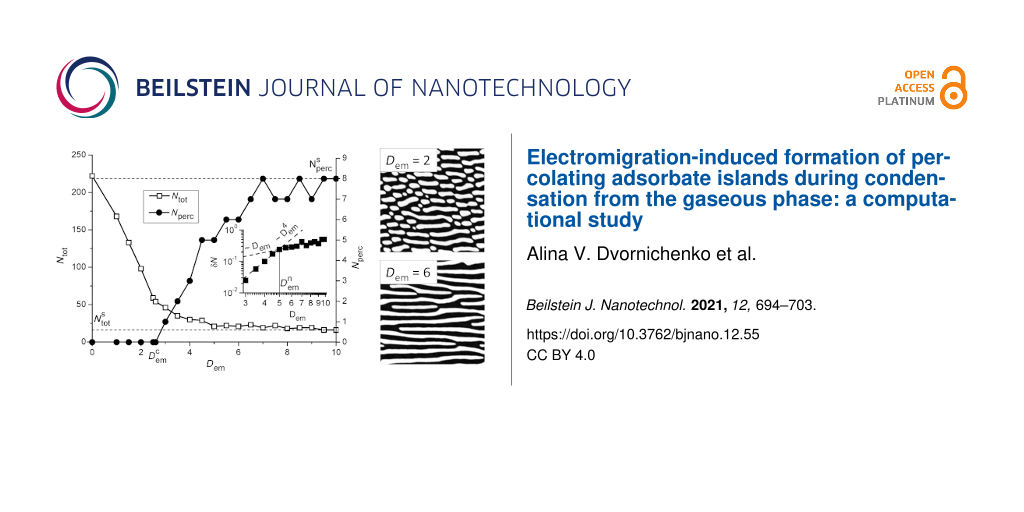
Next, we will discuss the influence of the electromigration effects on a change in surface morphology. To that end we fix α = 0.06 and k∥ = 0.1, at which in an isotropic system separated adsorbate islands are formed (see top snapshot in Figure 4). Typical snapshots of the quasistationary surface patterns (at t = 500) for different values of the electrical field strength Dem are shown in Figure 6a. It follows, that the applied electrical field with small strength provides the formation of elongated patterns in the field direction (see the snapshot at Dem = 2). An increase in the strength of the electric field Dem results in the formation of percolating adsorbate clusters and their number increases with Dem (compare snapshots at Dem = 4, 6 and 8 in Figure 6a). Temporal evolution of the mean adsorbate concentration ⟨x⟩ and dispersion ⟨(δx)2⟩ shown in Figure 6b indicates that patterns in Figure 6a are stationary ones. Moreover, it is seen that the electrical strength does not affect crucially both mean adsorbate concentration values and dispersion.
![[2190-4286-12-55-6]](/bjnano/content/figures/2190-4286-12-55-6.png?scale=2.0&max-width=1024&background=FFFFFF)
Figure 6: Typical snapshots of the quasistationary surface patterns for different values of the electrical field strength Dem at k∥ = 0.1 and α = 0.06 (a) and evolution of the mean adsorbate concentration ⟨x⟩ and the dispersion ⟨(δx)2⟩ (b).
Figure 6: Typical snapshots of the quasistationary surface patterns for different values of the electrical fi...
In Figure 7 we show the dependencies of the total amount of adsorbate clusters Ntot (empty squares) and number of percolating clusters Nperc (filled circles) on the electrical field strength Dem. It is seen, that Ntot decreases with growing Dem and at elevated values of the electric field strength Ntot attains the value ![[Graphic 19]](/bjnano/content/inline/2190-4286-12-55-i26.svg?max-width=637&scale=1.18182) > 1. If Dem becomes larger, at some critical value
> 1. If Dem becomes larger, at some critical value ![[Graphic 20]](/bjnano/content/inline/2190-4286-12-55-i27.svg?max-width=637&scale=1.18182) (α,k∥,ε,β) the number of percolating clusters Nperc starts to increase from zero and attains the value
(α,k∥,ε,β) the number of percolating clusters Nperc starts to increase from zero and attains the value ![[Graphic 21]](/bjnano/content/inline/2190-4286-12-55-i28.svg?max-width=637&scale=1.18182) . One can expect that at large Dem one will get
. One can expect that at large Dem one will get ![[Graphic 22]](/bjnano/content/inline/2190-4286-12-55-i29.svg?max-width=637&scale=1.18182) , when all adsorbate islands formed on the substrate will connect the opposite sides of the substrate. In the inset in Figure 7 we show the dependence of the ratio δN = Nperc/Ntot on the electrical field strength Dem on a log–log scale. It follows, that in the interval Dem ∈ (
, when all adsorbate islands formed on the substrate will connect the opposite sides of the substrate. In the inset in Figure 7 we show the dependence of the ratio δN = Nperc/Ntot on the electrical field strength Dem on a log–log scale. It follows, that in the interval Dem ∈ (![[Graphic 23]](/bjnano/content/inline/2190-4286-12-55-i30.svg?max-width=637&scale=1.18182) ) one gets the rapid growth of the dependence δN(Dem) with the asymptote
) one gets the rapid growth of the dependence δN(Dem) with the asymptote ![[Graphic 24]](/bjnano/content/inline/2190-4286-12-55-i31.svg?max-width=637&scale=1.18182) . This dynamics is realized due to separated elongated adsorbate clusters formed at Dem <
. This dynamics is realized due to separated elongated adsorbate clusters formed at Dem < ![[Graphic 25]](/bjnano/content/inline/2190-4286-12-55-i32.svg?max-width=637&scale=1.18182) starting to combine into percolating clusters (see snapshots at Dem = 2 and Dem = 4 in Figure 6). At elevated Dem >
starting to combine into percolating clusters (see snapshots at Dem = 2 and Dem = 4 in Figure 6). At elevated Dem > ![[Graphic 26]](/bjnano/content/inline/2190-4286-12-55-i33.svg?max-width=637&scale=1.18182) one gets a slow growth of the number of percolating adsorbate clusters (see filled circles in Figure 7) and asymptotic growth to δN ∝ Dem occurs.
one gets a slow growth of the number of percolating adsorbate clusters (see filled circles in Figure 7) and asymptotic growth to δN ∝ Dem occurs.
![[2190-4286-12-55-7]](/bjnano/content/figures/2190-4286-12-55-7.png?scale=2.0&max-width=1024&background=FFFFFF)
Figure 7: Dependencies of the total amount of adsorbate clusters Ntot and number of percolating clusters Nperc on the electrical field strength Dem at k∥ = 0.1 and α = 0.06. The inset shows a dependence of the ratio δN = Nperc/Ntot on the electrical field strength Dem.
Figure 7: Dependencies of the total amount of adsorbate clusters Ntot and number of percolating clusters Nperc...
Next, let us discuss the dependence of the critical value of the electric field strength ![[Graphic 27]](/bjnano/content/inline/2190-4286-12-55-i34.svg?max-width=637&scale=1.18182) , at which the percolating clusters of adsorbate begin to organize during deposition, on the adsorption coefficient α and the rate of the transference of adatoms between neighboring layers k∥. The corresponding dependencies
, at which the percolating clusters of adsorbate begin to organize during deposition, on the adsorption coefficient α and the rate of the transference of adatoms between neighboring layers k∥. The corresponding dependencies ![[Graphic 28]](/bjnano/content/inline/2190-4286-12-55-i35.svg?max-width=637&scale=1.18182) (α) at different k∥ are shown in Figure 8.
(α) at different k∥ are shown in Figure 8.
![[2190-4286-12-55-8]](/bjnano/content/figures/2190-4286-12-55-8.png?scale=2.0&max-width=1024&background=FFFFFF)
Figure 8:
Dependence of the critical value of the electrical field strength ![[Graphic 29]](/bjnano/content/inline/2190-4286-12-55-i36.svg?max-width=637&scale=1.18182) on the adsorption coefficient α at different values of the vertical diffusion coefficient k∥.
on the adsorption coefficient α at different values of the vertical diffusion coefficient k∥.
Figure 8:
Dependence of the critical value of the electrical field strength on the adsorption coefficient α ...
Let us initially discuss results for the case k∥ = 0.1, shown by filled squares in Figure 8. It follows that with an increase in the adsorption coefficient α from αc to αm (see Figure 4) the critical value of the strength of the applied electric field falls down to zero from the fixed value ![[Graphic 30]](/bjnano/content/inline/2190-4286-12-55-i37.svg?max-width=637&scale=1.18182) (k∥,ε,β). Hence, an increase in adsorption coefficient requires a smaller value of the strength of the applied electric field for the formation of percolating adsorbate clusters, which are realized above the dependence
(k∥,ε,β). Hence, an increase in adsorption coefficient requires a smaller value of the strength of the applied electric field for the formation of percolating adsorbate clusters, which are realized above the dependence ![[Graphic 31]](/bjnano/content/inline/2190-4286-12-55-i38.svg?max-width=637&scale=1.18182) (α). It seems natural that an increase in α leads to a growth in the concentration of adsorbate on the substrate. In such a case the separated islands in an isotropic system become large and closely located. Therefore, at elevated α < αm even a small strength of the applied electric force can induce the formation of percolating clusters.
(α). It seems natural that an increase in α leads to a growth in the concentration of adsorbate on the substrate. In such a case the separated islands in an isotropic system become large and closely located. Therefore, at elevated α < αm even a small strength of the applied electric force can induce the formation of percolating clusters.
An increase in the rate of adatoms transference between layers k∥ provides a decrease in adsorbate concentration on a substrate, and, as a result, requires elevated values of the strength of the applied electric force for the formation of percolating adsorbate clusters (see filled circles in Figure 8 at k∥ = 0.2). Obtained numerical data shown by filled symbols are fitted well by the exponential function exp(−α/α0) with the scaling parameter α0(k∥) (solid curves).
Finally, let us discuss an important question from the applied physics perspective about the stability of the elongated morphology of the adsorbate islands when the electric field is turned off. To this end we fix k∥ = 0.1 and α = 0.06 and as initial conditions for the coverage field x(r) use the configuration obtained at Dem = 6 for t = 500 (see the corresponding snapshot in Figure 6a). Next, we solve the Equation 4 with the same values of the control parameters at Dem = 0. The obtained results are shown in Figure 9. From Figure 9a it follows, that after the electric field is turned off the morphology of the surface patterns (formed with applied electric field) does not change. The temporal dependencies of both the mean adsorbate concentration ⟨x⟩ and the dispersion ⟨(δx)2⟩ (shown in Figure 9b with the applied electric field at t < 500 and without electric field at t > 500) illustrate that after the electric field is turned off both quantities dot not change in time. In the inset in the bottom panel in Figure 9b we show the power spectral density function f(κ) for the initial (t = 500), intermediate (t = 750) and final (t = 1000) stages rescaled by the maximal value fmax for the case t = 500. It follows, that the position of the peak of f(κ) does not change meaning that the period of spatial modulations of the coverage field x(r) remains constant. Hence, the elongated morphology of adsorbate islands remains stable if the electric field is turned off.
![[2190-4286-12-55-9]](/bjnano/content/figures/2190-4286-12-55-9.png?scale=2.0&max-width=1024&background=FFFFFF)
Figure 9: (a) Typical snapshots of the system evolution after the electric field is turned off at k∥ = 0.1, α = 0.06. The first snapshot corresponds to the case Dem = 6. (b) Evolution of the mean adsorbate concentration ⟨x⟩ (top panel) and the dispersion ⟨(δx)2⟩ (bottom panel). The inset in Figure 9b shows the power spectral density function for the different times of deposition after the electric field is turned off.
Figure 9: (a) Typical snapshots of the system evolution after the electric field is turned off at k∥ = 0.1, α...
Estimations
In order to test the parameter space used in our numerical simulations to offer a guidance for designing the corresponding experiments to observe patterns like the ones predicted by simulations we use the data from [78] for the system Ge on SiO2 at T = 773 K: activation energy for desorption Ed ≃ 0.44 eV and activation energy for diffusion ED ≃ 0.24 eV. By exploiting the formula for the diffusion length LD = ![[Graphic 32]](/bjnano/content/inline/2190-4286-12-55-i39.svg?max-width=637&scale=1.18182) with the lattice constant a = 5.6 × 10⁻¹⁰ for Ge we get LD = a2exp((Ed − ED)/T) ≃ 50 nm. With the used relation L = 40LD, the mean linear size (diameter) of circular stationary adsorbate islands in the isotropic case with Dem = 0, shown in the top panel in Figure 3b, and the transverse size of elongated structures at Dem ≠ 0, shown in Figure 6a, are about 2LD ≃ 100 nm. This is in good agreement with the experimental results discussed in [15,78].
with the lattice constant a = 5.6 × 10⁻¹⁰ for Ge we get LD = a2exp((Ed − ED)/T) ≃ 50 nm. With the used relation L = 40LD, the mean linear size (diameter) of circular stationary adsorbate islands in the isotropic case with Dem = 0, shown in the top panel in Figure 3b, and the transverse size of elongated structures at Dem ≠ 0, shown in Figure 6a, are about 2LD ≃ 100 nm. This is in good agreement with the experimental results discussed in [15,78].
Conclusion
In this article we have studied the effects of electromigration on the morphology of growing thin films during condensation from the gaseous phase in the framework of numerical simulations. It is shown that an increase in the strength of the electrical field applied to the substrate results in the formation of elongated adsorbate islands in the direction of the electric field. If the field strength exceeds a critical value depending on the control parameters, then the adsorbate self-organizes into percolating islands on the substrate. We have shown that the critical value of the strength of the applied electrical field falls exponentially with the adsorption coefficient. An increase in the rate of adsorbate transfer between neighboring layers requires larger values of the electrical field strength for the formation of percolating islands on a substrate. It is shown that the elongated morphology of adsorbate islands remains stable if the electric field is turned off.
The general results obtained within this work can be used to predict the morphology of nanostructured thin films formed during condensation from the gaseous phase. The dimensionless control parameters of the model can be rescaled with the help of experimental data for any kind of system adsorbate/substrate to adjust the technological conditions for the growth of the nanostructured thin films with specified morphology and statistical characteristics.
References
-
Black, J. R. IEEE Trans. Electron Devices 1969, 16, 338. doi:10.1109/t-ed.1969.16754
Return to citation in text: [1] [2] -
Ho, P. S.; Kwok, T. Rep. Prog. Phys. 1989, 52, 301. doi:10.1088/0034-4885/52/3/002
Return to citation in text: [1] [2] -
Tu, K. N. J. Appl. Phys. 2003, 94, 5451. doi:10.1063/1.1611263
Return to citation in text: [1] -
Choi, W. J.; Yeh, E. C. C.; Tu, K. N. J. Appl. Phys. 2003, 94, 5665. doi:10.1063/1.1616993
Return to citation in text: [1] -
Chiang, K. N.; Lee, C. C.; Lee, C. C.; Chen, K. M. Appl. Phys. Lett. 2006, 88, 072102. doi:10.1063/1.2173710
Return to citation in text: [1] -
Chen, C.; Tong, H. M.; Tu, K. N. Annu. Rev. Mater. Res. 2010, 40, 531. doi:10.1146/annurev.matsci.38.060407.130253
Return to citation in text: [1] -
Tian, T.; Chen, K.; MacDowell, A. A.; Parkinson, D.; Lai, Y.-S.; Tu, K. N. Scr. Mater. 2011, 65, 646. doi:10.1016/j.scriptamat.2011.07.002
Return to citation in text: [1] -
Homma, Y.; Mcclelland, R. J.; Hibino, H. Jpn. J. Appl. Phys., Part 2 1990, 29, L2254. doi:10.1143/jjap.29.l2254
Return to citation in text: [1] -
Williams, E. D.; Fu, E.; Yang, Y.-N.; Kandel, D.; Weeks, J. D. Surf. Sci. 1995, 336, L746. doi:10.1016/0039-6028(95)00551-x
Return to citation in text: [1] -
Gibbons, B. J.; Noffsinger, J.; Pelz, J. P. Surf. Sci. 2005, 575, L51. doi:10.1016/j.susc.2004.11.020
Return to citation in text: [1] -
Lin, S.-k.; Liu, Y.-c.; Chiu, S.-J.; Liu, Y.-T.; Lee, H.-Y. Sci. Rep. 2017, 7, 3082. doi:10.1038/s41598-017-03324-5
Return to citation in text: [1] -
Leroy, F.; Karashanova, D.; Dufay, M.; Debierre, J.-M.; Frisch, T.; Métois, J.-J.; Müller, P. Surf. Sci. 2009, 603, 507. doi:10.1016/j.susc.2008.12.016
Return to citation in text: [1] -
Usov, V.; Coileain, C. O.; Shvets, I. V. Phys. Rev. B 2010, 82, 153301. doi:10.1103/physrevb.82.153301
Return to citation in text: [1] -
Toktarbaiuly, O.; Usov, V.; Ó Coileáin, C.; Siewierska, K.; Krasnikov, S.; Norton, E.; Bozhko, S. I.; Semenov, V. N.; Chaika, A. N.; Murphy, B. E.; Lübben, O.; Krzyżewski, F.; Załuska-Kotur, M. A.; Krasteva, A.; Popova, H.; Tonchev, V.; Shvets, I. V. Phys. Rev. B 2018, 97, 035436. doi:10.1103/physrevb.97.035436
Return to citation in text: [1] -
Shklyaev, A. A.; Latyshev, A. V. Appl. Surf. Sci. 2019, 465, 10. doi:10.1016/j.apsusc.2018.09.119
Return to citation in text: [1] [2] -
Voigtländer, B. Surf. Sci. Rep. 2001, 43, 127. doi:10.1016/s0167-5729(01)00012-7
Return to citation in text: [1] -
Shklyaev, A. A.; Ichikawa, M. Phys.-Usp. 2008, 51, 133. doi:10.1070/pu2008v051n02abeh006344
Return to citation in text: [1] -
Shklyaev, A. A.; Romanyuk, K. N.; Kosolobov, S. S. Surf. Sci. 2014, 625, 50. doi:10.1016/j.susc.2014.03.013
Return to citation in text: [1] -
Teys, S. A. Appl. Surf. Sci. 2017, 392, 1017. doi:10.1016/j.apsusc.2016.09.124
Return to citation in text: [1] -
MacLeod, J. M.; Lipton-Duffin, J. A.; Lanke, U.; Urquhart, S. G.; Rosei, F. Appl. Phys. Lett. 2009, 94, 103109. doi:10.1063/1.3093674
Return to citation in text: [1] -
Shklyaev, A.; Bolotov, L.; Poborchii, V.; Tada, T. J. Appl. Phys. 2015, 117, 205303. doi:10.1063/1.4921596
Return to citation in text: [1] -
Yongsunthon, R.; Tao, C.; Rous, P.; Williams, E. D. Surface Electromigration and Current Crowding. In Nanophenomena at Surfaces; Michailov, M., Ed.; Springer Series in Surface Sciences, Vol. 47; Springer-Verlag: Berlin Heidelberg, 2011; pp 113–143. doi:10.1007/978-3-642-16510-8_5
Return to citation in text: [1] [2] -
Tao, C.; Cullen, W. G.; Williams, E. D. Science 2010, 328, 736. doi:10.1126/science.1186648
Return to citation in text: [1] [2] -
Los Santos Valladares, L. D.; Leon Felix, L.; Bustamante Dominguez, A.; Mitrelias, T.; Sfigakis, F.; Khondaker, S. I.; Barnes, C. H. W.; Majima, Y. Nanotechnology 2010, 21, 445304. doi:10.1088/0957-4484/21/44/445304
Return to citation in text: [1] -
Gardinowski, G.; Schmeidel, J.; Pfnür, H.; Block, T.; Tegenkamp, C. Appl. Phys. Lett. 2006, 89, 063120. doi:10.1063/1.2336650
Return to citation in text: [1] -
Curiotto, S.; Müller, P.; El-Barraj, A.; Cheynis, F.; Pierre-Louis, O.; Leroy, F. Appl. Surf. Sci. 2019, 469, 463. doi:10.1016/j.apsusc.2018.11.049
Return to citation in text: [1] [2] -
Zhao, J.; Yu, R.; Dai, S.; Zhu, J. Surf. Sci. 2014, 625, 10. doi:10.1016/j.susc.2014.02.018
Return to citation in text: [1] -
Stoyanov, S. Surf. Sci. 1997, 370, 345. doi:10.1016/s0039-6028(96)00966-1
Return to citation in text: [1] -
Dufay, M.; Debierre, J.-M.; Frisch, T. Phys. Rev. B 2007, 75, 045413. doi:10.1103/physrevb.75.045413
Return to citation in text: [1] -
Chang, J.; Pierre-Louis, O.; Misbah, C. Phys. Rev. Lett. 2006, 96, 195901. doi:10.1103/physrevlett.96.195901
Return to citation in text: [1] -
Pierre-Louis, O. Phys. Rev. Lett. 2006, 96, 135901. doi:10.1103/physrevlett.96.135901
Return to citation in text: [1] -
Krug, J.; Dobbs, H. T. Phys. Rev. Lett. 1994, 73, 1947. doi:10.1103/physrevlett.73.1947
Return to citation in text: [1] -
Schimschak, M.; Krug, J. Phys. Rev. Lett. 1997, 78, 278. doi:10.1103/physrevlett.78.278
Return to citation in text: [1] -
Du, D.; Srolovitz, D. Appl. Phys. Lett. 2004, 85, 4917. doi:10.1063/1.1826233
Return to citation in text: [1] -
Barakat, F.; Martens, K.; Pierre-Louis, O. Phys. Rev. Lett. 2012, 109, 056101. doi:10.1103/physrevlett.109.056101
Return to citation in text: [1] -
Quah, J.; Margetis, D. Multiscale Model. Simul. 2010, 8, 667. doi:10.1137/090760635
Return to citation in text: [1] -
Leroy, F.; Müller, P.; Métois, J. J.; Pierre-Louis, O. Phys. Rev. B 2007, 76, 045402. doi:10.1103/physrevb.76.045402
Return to citation in text: [1] -
Chiu, C.-H.; Huang, Z.; Poh, C. T. Phys. Rev. B 2006, 73, 193409. doi:10.1103/physrevb.73.193409
Return to citation in text: [1] -
Maroudas, D. Surf. Sci. Rep. 2011, 66, 299. doi:10.1016/j.surfrep.2011.05.001
Return to citation in text: [1] -
Tomar, V.; Gungor, M. R.; Maroudas, D. Phys. Rev. Lett. 2008, 100, 036106. doi:10.1103/physrevlett.100.036106
Return to citation in text: [1] -
Khenner, M. C. R. Phys. 2013, 14, 607. doi:10.1016/j.crhy.2013.06.009
Return to citation in text: [1] -
Kim, J. H.; Srolovitz, D. J.; Cha, P.-R.; Yoon, J.-K. J. Appl. Phys. 2006, 100, 054502. doi:10.1063/1.2336488
Return to citation in text: [1] -
Du, L.; Maroudas, D. J. Appl. Phys. 2018, 124, 125302. doi:10.1063/1.5047405
Return to citation in text: [1] -
Kuhn, P.; Krug, J.; Hausser, F.; Voigt, A. Phys. Rev. Lett. 2005, 94, 166105. doi:10.1103/physrevlett.94.166105
Return to citation in text: [1] -
Dasgupta, D.; Maroudas, D. Appl. Phys. Lett. 2013, 103, 181602. doi:10.1063/1.4827304
Return to citation in text: [1] -
Dasgupta, D.; Kumar, A.; Maroudas, D. Surf. Sci. 2018, 669, 25. doi:10.1016/j.susc.2017.10.027
Return to citation in text: [1] -
Kumar, A.; Dasgupta, D.; Dimitrakopoulos, C.; Maroudas, D. Appl. Phys. Lett. 2016, 108, 193109. doi:10.1063/1.4949333
Return to citation in text: [1] -
Solenov, D.; Velizhanin, K. A. Phys. Rev. Lett. 2012, 109, 095504. doi:10.1103/physrevlett.109.095504
Return to citation in text: [1] -
Casal, S. B.; Wio, H. S.; Mangioni, S. Phys. A (Amsterdam, Neth.) 2002, 311, 443. doi:10.1016/s0378-4371(02)00828-2
Return to citation in text: [1] [2] -
Kharchenko, V. O.; Kharchenko, D. O. Phys. Rev. E 2012, 86, 041143. doi:10.1103/physreve.86.041143
Return to citation in text: [1] [2] [3] -
Mangioni, S. E.; Wio, H. S. Phys. Rev. E 2005, 71, 056203. doi:10.1103/physreve.71.056203
Return to citation in text: [1] [2] -
Mangioni, S. E. Phys. A (Amsterdam, Neth.) 2010, 389, 1799. doi:10.1016/j.physa.2010.01.011
Return to citation in text: [1] [2] -
Mikhailov, A.; Ertl, G. Chem. Phys. Lett. 1995, 238, 104. doi:10.1016/0009-2614(95)00386-x
Return to citation in text: [1] [2] [3] [4] -
Battogtokh, D.; Hildebrand, M.; Krischer, K.; Mikhailov, A. S. Phys. Rep. 1997, 288, 435. doi:10.1016/s0370-1573(97)00036-7
Return to citation in text: [1] [2] [3] [4] -
Hildebrand, M.; Mikhailov, A. S.; Ertl, G. Phys. Rev. Lett. 1998, 81, 2602. doi:10.1103/physrevlett.81.2602
Return to citation in text: [1] [2] [3] [4] [5] -
Hildebrand, M.; Mikhailov, A. S.; Ertl, G. Phys. Rev. E 1998, 58, 5483. doi:10.1103/physreve.58.5483
Return to citation in text: [1] [2] [3] [4] [5] -
Walgraef, D. Phys. E (Amsterdam, Neth.) 2003, 18, 393. doi:10.1016/s1386-9477(02)01104-9
Return to citation in text: [1] [2] [3] [4] -
Walgraef, D. Int. J. Quantum Chem. 2004, 98, 248. doi:10.1002/qua.10877
Return to citation in text: [1] [2] [3] [4] -
Kharchenko, V. O.; Kharchenko, D. O.; Kokhan, S. V.; Vernyhora, I. V.; Yanovsky, V. V. Phys. Scr. 2012, 86, 055401. doi:10.1088/0031-8949/86/05/055401
Return to citation in text: [1] [2] [3] [4] [5] -
Kharchenko, V. O.; Kharchenko, D. O.; Dvornichenko, A. V. Surf. Sci. 2014, 630, 158. doi:10.1016/j.susc.2014.08.008
Return to citation in text: [1] [2] [3] -
Walgraef, D. Phys. E (Amsterdam, Neth.) 2002, 15, 33. doi:10.1016/s1386-9477(01)00492-1
Return to citation in text: [1] [2] -
Kharchenko, V. O.; Dvornichenko, A. V.; Borysiuk, V. N. Eur. Phys. J. B 2018, 91, 93. doi:10.1140/epjb/e2018-80730-8
Return to citation in text: [1] [2] [3] -
Kharchenko, V. O.; Dvornichenko, A. V.; Zhylenko, T. I. Appl. Nanosci. 2020, 10, 2535. doi:10.1007/s13204-019-01091-5
Return to citation in text: [1] [2] [3] [4] -
Dvornichenko, A. V.; Kharchenko, V. O. Phys. Lett. A 2020, 384, 126329. doi:10.1016/j.physleta.2020.126329
Return to citation in text: [1] [2] -
Kharchenko, V. O.; Kharchenko, D. O.; Dvornichenko, A. V. Phys. A (Amsterdam, Neth.) 2016, 444, 689. doi:10.1016/j.physa.2015.10.056
Return to citation in text: [1] -
Kharchenko, D. O.; Kharchenko, V. O.; Lysenko, I. O. Phys. Scr. 2011, 83, 045802. doi:10.1088/0031-8949/83/04/045802
Return to citation in text: [1] -
Kharchenko, D. O.; Kharchenko, V. O.; Zhylenko, T.; Dvornichenko, A. V. Eur. Phys. J. B 2013, 86, 175. doi:10.1140/epjb/e2013-31053-1
Return to citation in text: [1] -
Kharchenko, V. O.; Kharchenko, D. O.; Dvornichenko, A. V. Eur. Phys. J. B 2015, 88, 3. doi:10.1140/epjb/e2014-50327-6
Return to citation in text: [1] -
Kharchenko, V. O.; Kharchenko, D. O. Eur. Phys. J. B 2012, 85, 383. doi:10.1140/epjb/e2012-30522-3
Return to citation in text: [1] -
Kharchenko, V. O.; Kharchenko, D. O. Condens. Matter Phys. 2013, 16, 33001. doi:10.5488/cmp.16.33001
Return to citation in text: [1] -
Kharchenko, D. O.; Kharchenko, V. O.; Bashtova, A. I. Radiat. Eff. Defects Solids 2014, 169, 418. doi:10.1080/10420150.2014.905577
Return to citation in text: [1] -
Kharchenko, V. O.; Kharchenko, D. O. Phys. Rev. E 2014, 89, 042133. doi:10.1103/physreve.89.042133
Return to citation in text: [1] -
Kharchenko, D. O.; Kharchenko, V. O.; Bashtova, A. I. Ukr. J. Phys. 2013, 58, 993. doi:10.15407/ujpe58.10.0993
Return to citation in text: [1] -
Sfyris, G. I.; Gungor, M. R.; Maroudas, D. Appl. Phys. Lett. 2010, 96, 231911. doi:10.1063/1.3447371
Return to citation in text: [1] -
Zauderer, E. Partial Differential Equations of Applied Mathematics; John Wiley & Sons, Inc.: Hoboken, NJ, U.S.A., 2006. doi:10.1002/9781118033302
Return to citation in text: [1] -
Grindrod, P. The Theory and Applications of Reaction-Diffusion Equations; Oxford University Press, 1996.
Return to citation in text: [1] -
Hundsdorfer, W.; Verwer, J. Numerical Solution of Time-Dependent Advection-Diffusion-Reaction Equations; Springer Series in Computational Mathematics; Springer Berlin: Berlin, Germany, 2003. doi:10.1007/978-3-662-09017-6
Return to citation in text: [1] -
Leonhardt, D.; Han, S. M. Surf. Sci. 2009, 603, 2624. doi:10.1016/j.susc.2009.06.015
Return to citation in text: [1] [2]
| 66. | Kharchenko, D. O.; Kharchenko, V. O.; Lysenko, I. O. Phys. Scr. 2011, 83, 045802. doi:10.1088/0031-8949/83/04/045802 |
| 67. | Kharchenko, D. O.; Kharchenko, V. O.; Zhylenko, T.; Dvornichenko, A. V. Eur. Phys. J. B 2013, 86, 175. doi:10.1140/epjb/e2013-31053-1 |
| 68. | Kharchenko, V. O.; Kharchenko, D. O.; Dvornichenko, A. V. Eur. Phys. J. B 2015, 88, 3. doi:10.1140/epjb/e2014-50327-6 |
| 69. | Kharchenko, V. O.; Kharchenko, D. O. Eur. Phys. J. B 2012, 85, 383. doi:10.1140/epjb/e2012-30522-3 |
| 70. | Kharchenko, V. O.; Kharchenko, D. O. Condens. Matter Phys. 2013, 16, 33001. doi:10.5488/cmp.16.33001 |
| 71. | Kharchenko, D. O.; Kharchenko, V. O.; Bashtova, A. I. Radiat. Eff. Defects Solids 2014, 169, 418. doi:10.1080/10420150.2014.905577 |
| 72. | Kharchenko, V. O.; Kharchenko, D. O. Phys. Rev. E 2014, 89, 042133. doi:10.1103/physreve.89.042133 |
| 73. | Kharchenko, D. O.; Kharchenko, V. O.; Bashtova, A. I. Ukr. J. Phys. 2013, 58, 993. doi:10.15407/ujpe58.10.0993 |
| 74. | Sfyris, G. I.; Gungor, M. R.; Maroudas, D. Appl. Phys. Lett. 2010, 96, 231911. doi:10.1063/1.3447371 |
| 1. | Black, J. R. IEEE Trans. Electron Devices 1969, 16, 338. doi:10.1109/t-ed.1969.16754 |
| 2. | Ho, P. S.; Kwok, T. Rep. Prog. Phys. 1989, 52, 301. doi:10.1088/0034-4885/52/3/002 |
| 12. | Leroy, F.; Karashanova, D.; Dufay, M.; Debierre, J.-M.; Frisch, T.; Métois, J.-J.; Müller, P. Surf. Sci. 2009, 603, 507. doi:10.1016/j.susc.2008.12.016 |
| 13. | Usov, V.; Coileain, C. O.; Shvets, I. V. Phys. Rev. B 2010, 82, 153301. doi:10.1103/physrevb.82.153301 |
| 32. | Krug, J.; Dobbs, H. T. Phys. Rev. Lett. 1994, 73, 1947. doi:10.1103/physrevlett.73.1947 |
| 33. | Schimschak, M.; Krug, J. Phys. Rev. Lett. 1997, 78, 278. doi:10.1103/physrevlett.78.278 |
| 34. | Du, D.; Srolovitz, D. Appl. Phys. Lett. 2004, 85, 4917. doi:10.1063/1.1826233 |
| 35. | Barakat, F.; Martens, K.; Pierre-Louis, O. Phys. Rev. Lett. 2012, 109, 056101. doi:10.1103/physrevlett.109.056101 |
| 36. | Quah, J.; Margetis, D. Multiscale Model. Simul. 2010, 8, 667. doi:10.1137/090760635 |
| 37. | Leroy, F.; Müller, P.; Métois, J. J.; Pierre-Louis, O. Phys. Rev. B 2007, 76, 045402. doi:10.1103/physrevb.76.045402 |
| 8. | Homma, Y.; Mcclelland, R. J.; Hibino, H. Jpn. J. Appl. Phys., Part 2 1990, 29, L2254. doi:10.1143/jjap.29.l2254 |
| 9. | Williams, E. D.; Fu, E.; Yang, Y.-N.; Kandel, D.; Weeks, J. D. Surf. Sci. 1995, 336, L746. doi:10.1016/0039-6028(95)00551-x |
| 10. | Gibbons, B. J.; Noffsinger, J.; Pelz, J. P. Surf. Sci. 2005, 575, L51. doi:10.1016/j.susc.2004.11.020 |
| 11. | Lin, S.-k.; Liu, Y.-c.; Chiu, S.-J.; Liu, Y.-T.; Lee, H.-Y. Sci. Rep. 2017, 7, 3082. doi:10.1038/s41598-017-03324-5 |
| 38. | Chiu, C.-H.; Huang, Z.; Poh, C. T. Phys. Rev. B 2006, 73, 193409. doi:10.1103/physrevb.73.193409 |
| 39. | Maroudas, D. Surf. Sci. Rep. 2011, 66, 299. doi:10.1016/j.surfrep.2011.05.001 |
| 40. | Tomar, V.; Gungor, M. R.; Maroudas, D. Phys. Rev. Lett. 2008, 100, 036106. doi:10.1103/physrevlett.100.036106 |
| 41. | Khenner, M. C. R. Phys. 2013, 14, 607. doi:10.1016/j.crhy.2013.06.009 |
| 3. | Tu, K. N. J. Appl. Phys. 2003, 94, 5451. doi:10.1063/1.1611263 |
| 4. | Choi, W. J.; Yeh, E. C. C.; Tu, K. N. J. Appl. Phys. 2003, 94, 5665. doi:10.1063/1.1616993 |
| 5. | Chiang, K. N.; Lee, C. C.; Lee, C. C.; Chen, K. M. Appl. Phys. Lett. 2006, 88, 072102. doi:10.1063/1.2173710 |
| 6. | Chen, C.; Tong, H. M.; Tu, K. N. Annu. Rev. Mater. Res. 2010, 40, 531. doi:10.1146/annurev.matsci.38.060407.130253 |
| 7. | Tian, T.; Chen, K.; MacDowell, A. A.; Parkinson, D.; Lai, Y.-S.; Tu, K. N. Scr. Mater. 2011, 65, 646. doi:10.1016/j.scriptamat.2011.07.002 |
| 27. | Zhao, J.; Yu, R.; Dai, S.; Zhu, J. Surf. Sci. 2014, 625, 10. doi:10.1016/j.susc.2014.02.018 |
| 15. | Shklyaev, A. A.; Latyshev, A. V. Appl. Surf. Sci. 2019, 465, 10. doi:10.1016/j.apsusc.2018.09.119 |
| 78. | Leonhardt, D.; Han, S. M. Surf. Sci. 2009, 603, 2624. doi:10.1016/j.susc.2009.06.015 |
| 1. | Black, J. R. IEEE Trans. Electron Devices 1969, 16, 338. doi:10.1109/t-ed.1969.16754 |
| 2. | Ho, P. S.; Kwok, T. Rep. Prog. Phys. 1989, 52, 301. doi:10.1088/0034-4885/52/3/002 |
| 28. | Stoyanov, S. Surf. Sci. 1997, 370, 345. doi:10.1016/s0039-6028(96)00966-1 |
| 29. | Dufay, M.; Debierre, J.-M.; Frisch, T. Phys. Rev. B 2007, 75, 045413. doi:10.1103/physrevb.75.045413 |
| 30. | Chang, J.; Pierre-Louis, O.; Misbah, C. Phys. Rev. Lett. 2006, 96, 195901. doi:10.1103/physrevlett.96.195901 |
| 31. | Pierre-Louis, O. Phys. Rev. Lett. 2006, 96, 135901. doi:10.1103/physrevlett.96.135901 |
| 20. | MacLeod, J. M.; Lipton-Duffin, J. A.; Lanke, U.; Urquhart, S. G.; Rosei, F. Appl. Phys. Lett. 2009, 94, 103109. doi:10.1063/1.3093674 |
| 21. | Shklyaev, A.; Bolotov, L.; Poborchii, V.; Tada, T. J. Appl. Phys. 2015, 117, 205303. doi:10.1063/1.4921596 |
| 24. | Los Santos Valladares, L. D.; Leon Felix, L.; Bustamante Dominguez, A.; Mitrelias, T.; Sfigakis, F.; Khondaker, S. I.; Barnes, C. H. W.; Majima, Y. Nanotechnology 2010, 21, 445304. doi:10.1088/0957-4484/21/44/445304 |
| 25. | Gardinowski, G.; Schmeidel, J.; Pfnür, H.; Block, T.; Tegenkamp, C. Appl. Phys. Lett. 2006, 89, 063120. doi:10.1063/1.2336650 |
| 63. | Kharchenko, V. O.; Dvornichenko, A. V.; Zhylenko, T. I. Appl. Nanosci. 2020, 10, 2535. doi:10.1007/s13204-019-01091-5 |
| 64. | Dvornichenko, A. V.; Kharchenko, V. O. Phys. Lett. A 2020, 384, 126329. doi:10.1016/j.physleta.2020.126329 |
| 16. | Voigtländer, B. Surf. Sci. Rep. 2001, 43, 127. doi:10.1016/s0167-5729(01)00012-7 |
| 17. | Shklyaev, A. A.; Ichikawa, M. Phys.-Usp. 2008, 51, 133. doi:10.1070/pu2008v051n02abeh006344 |
| 18. | Shklyaev, A. A.; Romanyuk, K. N.; Kosolobov, S. S. Surf. Sci. 2014, 625, 50. doi:10.1016/j.susc.2014.03.013 |
| 19. | Teys, S. A. Appl. Surf. Sci. 2017, 392, 1017. doi:10.1016/j.apsusc.2016.09.124 |
| 22. | Yongsunthon, R.; Tao, C.; Rous, P.; Williams, E. D. Surface Electromigration and Current Crowding. In Nanophenomena at Surfaces; Michailov, M., Ed.; Springer Series in Surface Sciences, Vol. 47; Springer-Verlag: Berlin Heidelberg, 2011; pp 113–143. doi:10.1007/978-3-642-16510-8_5 |
| 23. | Tao, C.; Cullen, W. G.; Williams, E. D. Science 2010, 328, 736. doi:10.1126/science.1186648 |
| 26. | Curiotto, S.; Müller, P.; El-Barraj, A.; Cheynis, F.; Pierre-Louis, O.; Leroy, F. Appl. Surf. Sci. 2019, 469, 463. doi:10.1016/j.apsusc.2018.11.049 |
| 78. | Leonhardt, D.; Han, S. M. Surf. Sci. 2009, 603, 2624. doi:10.1016/j.susc.2009.06.015 |
| 15. | Shklyaev, A. A.; Latyshev, A. V. Appl. Surf. Sci. 2019, 465, 10. doi:10.1016/j.apsusc.2018.09.119 |
| 55. | Hildebrand, M.; Mikhailov, A. S.; Ertl, G. Phys. Rev. Lett. 1998, 81, 2602. doi:10.1103/physrevlett.81.2602 |
| 56. | Hildebrand, M.; Mikhailov, A. S.; Ertl, G. Phys. Rev. E 1998, 58, 5483. doi:10.1103/physreve.58.5483 |
| 14. | Toktarbaiuly, O.; Usov, V.; Ó Coileáin, C.; Siewierska, K.; Krasnikov, S.; Norton, E.; Bozhko, S. I.; Semenov, V. N.; Chaika, A. N.; Murphy, B. E.; Lübben, O.; Krzyżewski, F.; Załuska-Kotur, M. A.; Krasteva, A.; Popova, H.; Tonchev, V.; Shvets, I. V. Phys. Rev. B 2018, 97, 035436. doi:10.1103/physrevb.97.035436 |
| 22. | Yongsunthon, R.; Tao, C.; Rous, P.; Williams, E. D. Surface Electromigration and Current Crowding. In Nanophenomena at Surfaces; Michailov, M., Ed.; Springer Series in Surface Sciences, Vol. 47; Springer-Verlag: Berlin Heidelberg, 2011; pp 113–143. doi:10.1007/978-3-642-16510-8_5 |
| 23. | Tao, C.; Cullen, W. G.; Williams, E. D. Science 2010, 328, 736. doi:10.1126/science.1186648 |
| 75. | Zauderer, E. Partial Differential Equations of Applied Mathematics; John Wiley & Sons, Inc.: Hoboken, NJ, U.S.A., 2006. doi:10.1002/9781118033302 |
| 76. | Grindrod, P. The Theory and Applications of Reaction-Diffusion Equations; Oxford University Press, 1996. |
| 77. | Hundsdorfer, W.; Verwer, J. Numerical Solution of Time-Dependent Advection-Diffusion-Reaction Equations; Springer Series in Computational Mathematics; Springer Berlin: Berlin, Germany, 2003. doi:10.1007/978-3-662-09017-6 |
| 26. | Curiotto, S.; Müller, P.; El-Barraj, A.; Cheynis, F.; Pierre-Louis, O.; Leroy, F. Appl. Surf. Sci. 2019, 469, 463. doi:10.1016/j.apsusc.2018.11.049 |
| 44. | Kuhn, P.; Krug, J.; Hausser, F.; Voigt, A. Phys. Rev. Lett. 2005, 94, 166105. doi:10.1103/physrevlett.94.166105 |
| 45. | Dasgupta, D.; Maroudas, D. Appl. Phys. Lett. 2013, 103, 181602. doi:10.1063/1.4827304 |
| 46. | Dasgupta, D.; Kumar, A.; Maroudas, D. Surf. Sci. 2018, 669, 25. doi:10.1016/j.susc.2017.10.027 |
| 47. | Kumar, A.; Dasgupta, D.; Dimitrakopoulos, C.; Maroudas, D. Appl. Phys. Lett. 2016, 108, 193109. doi:10.1063/1.4949333 |
| 42. | Kim, J. H.; Srolovitz, D. J.; Cha, P.-R.; Yoon, J.-K. J. Appl. Phys. 2006, 100, 054502. doi:10.1063/1.2336488 |
| 62. | Kharchenko, V. O.; Dvornichenko, A. V.; Borysiuk, V. N. Eur. Phys. J. B 2018, 91, 93. doi:10.1140/epjb/e2018-80730-8 |
| 63. | Kharchenko, V. O.; Dvornichenko, A. V.; Zhylenko, T. I. Appl. Nanosci. 2020, 10, 2535. doi:10.1007/s13204-019-01091-5 |
| 49. | Casal, S. B.; Wio, H. S.; Mangioni, S. Phys. A (Amsterdam, Neth.) 2002, 311, 443. doi:10.1016/s0378-4371(02)00828-2 |
| 50. | Kharchenko, V. O.; Kharchenko, D. O. Phys. Rev. E 2012, 86, 041143. doi:10.1103/physreve.86.041143 |
| 51. | Mangioni, S. E.; Wio, H. S. Phys. Rev. E 2005, 71, 056203. doi:10.1103/physreve.71.056203 |
| 52. | Mangioni, S. E. Phys. A (Amsterdam, Neth.) 2010, 389, 1799. doi:10.1016/j.physa.2010.01.011 |
| 53. | Mikhailov, A.; Ertl, G. Chem. Phys. Lett. 1995, 238, 104. doi:10.1016/0009-2614(95)00386-x |
| 54. | Battogtokh, D.; Hildebrand, M.; Krischer, K.; Mikhailov, A. S. Phys. Rep. 1997, 288, 435. doi:10.1016/s0370-1573(97)00036-7 |
| 55. | Hildebrand, M.; Mikhailov, A. S.; Ertl, G. Phys. Rev. Lett. 1998, 81, 2602. doi:10.1103/physrevlett.81.2602 |
| 56. | Hildebrand, M.; Mikhailov, A. S.; Ertl, G. Phys. Rev. E 1998, 58, 5483. doi:10.1103/physreve.58.5483 |
| 57. | Walgraef, D. Phys. E (Amsterdam, Neth.) 2003, 18, 393. doi:10.1016/s1386-9477(02)01104-9 |
| 58. | Walgraef, D. Int. J. Quantum Chem. 2004, 98, 248. doi:10.1002/qua.10877 |
| 59. | Kharchenko, V. O.; Kharchenko, D. O.; Kokhan, S. V.; Vernyhora, I. V.; Yanovsky, V. V. Phys. Scr. 2012, 86, 055401. doi:10.1088/0031-8949/86/05/055401 |
| 60. | Kharchenko, V. O.; Kharchenko, D. O.; Dvornichenko, A. V. Surf. Sci. 2014, 630, 158. doi:10.1016/j.susc.2014.08.008 |
| 61. | Walgraef, D. Phys. E (Amsterdam, Neth.) 2002, 15, 33. doi:10.1016/s1386-9477(01)00492-1 |
| 62. | Kharchenko, V. O.; Dvornichenko, A. V.; Borysiuk, V. N. Eur. Phys. J. B 2018, 91, 93. doi:10.1140/epjb/e2018-80730-8 |
| 63. | Kharchenko, V. O.; Dvornichenko, A. V.; Zhylenko, T. I. Appl. Nanosci. 2020, 10, 2535. doi:10.1007/s13204-019-01091-5 |
| 59. | Kharchenko, V. O.; Kharchenko, D. O.; Kokhan, S. V.; Vernyhora, I. V.; Yanovsky, V. V. Phys. Scr. 2012, 86, 055401. doi:10.1088/0031-8949/86/05/055401 |
| 53. | Mikhailov, A.; Ertl, G. Chem. Phys. Lett. 1995, 238, 104. doi:10.1016/0009-2614(95)00386-x |
| 54. | Battogtokh, D.; Hildebrand, M.; Krischer, K.; Mikhailov, A. S. Phys. Rep. 1997, 288, 435. doi:10.1016/s0370-1573(97)00036-7 |
| 55. | Hildebrand, M.; Mikhailov, A. S.; Ertl, G. Phys. Rev. Lett. 1998, 81, 2602. doi:10.1103/physrevlett.81.2602 |
| 56. | Hildebrand, M.; Mikhailov, A. S.; Ertl, G. Phys. Rev. E 1998, 58, 5483. doi:10.1103/physreve.58.5483 |
| 57. | Walgraef, D. Phys. E (Amsterdam, Neth.) 2003, 18, 393. doi:10.1016/s1386-9477(02)01104-9 |
| 58. | Walgraef, D. Int. J. Quantum Chem. 2004, 98, 248. doi:10.1002/qua.10877 |
| 59. | Kharchenko, V. O.; Kharchenko, D. O.; Kokhan, S. V.; Vernyhora, I. V.; Yanovsky, V. V. Phys. Scr. 2012, 86, 055401. doi:10.1088/0031-8949/86/05/055401 |
| 60. | Kharchenko, V. O.; Kharchenko, D. O.; Dvornichenko, A. V. Surf. Sci. 2014, 630, 158. doi:10.1016/j.susc.2014.08.008 |
| 65. | Kharchenko, V. O.; Kharchenko, D. O.; Dvornichenko, A. V. Phys. A (Amsterdam, Neth.) 2016, 444, 689. doi:10.1016/j.physa.2015.10.056 |
| 50. | Kharchenko, V. O.; Kharchenko, D. O. Phys. Rev. E 2012, 86, 041143. doi:10.1103/physreve.86.041143 |
| 59. | Kharchenko, V. O.; Kharchenko, D. O.; Kokhan, S. V.; Vernyhora, I. V.; Yanovsky, V. V. Phys. Scr. 2012, 86, 055401. doi:10.1088/0031-8949/86/05/055401 |
| 62. | Kharchenko, V. O.; Dvornichenko, A. V.; Borysiuk, V. N. Eur. Phys. J. B 2018, 91, 93. doi:10.1140/epjb/e2018-80730-8 |
| 63. | Kharchenko, V. O.; Dvornichenko, A. V.; Zhylenko, T. I. Appl. Nanosci. 2020, 10, 2535. doi:10.1007/s13204-019-01091-5 |
| 64. | Dvornichenko, A. V.; Kharchenko, V. O. Phys. Lett. A 2020, 384, 126329. doi:10.1016/j.physleta.2020.126329 |
| 53. | Mikhailov, A.; Ertl, G. Chem. Phys. Lett. 1995, 238, 104. doi:10.1016/0009-2614(95)00386-x |
| 54. | Battogtokh, D.; Hildebrand, M.; Krischer, K.; Mikhailov, A. S. Phys. Rep. 1997, 288, 435. doi:10.1016/s0370-1573(97)00036-7 |
| 55. | Hildebrand, M.; Mikhailov, A. S.; Ertl, G. Phys. Rev. Lett. 1998, 81, 2602. doi:10.1103/physrevlett.81.2602 |
| 56. | Hildebrand, M.; Mikhailov, A. S.; Ertl, G. Phys. Rev. E 1998, 58, 5483. doi:10.1103/physreve.58.5483 |
| 57. | Walgraef, D. Phys. E (Amsterdam, Neth.) 2003, 18, 393. doi:10.1016/s1386-9477(02)01104-9 |
| 58. | Walgraef, D. Int. J. Quantum Chem. 2004, 98, 248. doi:10.1002/qua.10877 |
| 48. | Solenov, D.; Velizhanin, K. A. Phys. Rev. Lett. 2012, 109, 095504. doi:10.1103/physrevlett.109.095504 |
| 49. | Casal, S. B.; Wio, H. S.; Mangioni, S. Phys. A (Amsterdam, Neth.) 2002, 311, 443. doi:10.1016/s0378-4371(02)00828-2 |
| 50. | Kharchenko, V. O.; Kharchenko, D. O. Phys. Rev. E 2012, 86, 041143. doi:10.1103/physreve.86.041143 |
| 51. | Mangioni, S. E.; Wio, H. S. Phys. Rev. E 2005, 71, 056203. doi:10.1103/physreve.71.056203 |
| 52. | Mangioni, S. E. Phys. A (Amsterdam, Neth.) 2010, 389, 1799. doi:10.1016/j.physa.2010.01.011 |
| 53. | Mikhailov, A.; Ertl, G. Chem. Phys. Lett. 1995, 238, 104. doi:10.1016/0009-2614(95)00386-x |
| 54. | Battogtokh, D.; Hildebrand, M.; Krischer, K.; Mikhailov, A. S. Phys. Rep. 1997, 288, 435. doi:10.1016/s0370-1573(97)00036-7 |
| 55. | Hildebrand, M.; Mikhailov, A. S.; Ertl, G. Phys. Rev. Lett. 1998, 81, 2602. doi:10.1103/physrevlett.81.2602 |
| 56. | Hildebrand, M.; Mikhailov, A. S.; Ertl, G. Phys. Rev. E 1998, 58, 5483. doi:10.1103/physreve.58.5483 |
| 57. | Walgraef, D. Phys. E (Amsterdam, Neth.) 2003, 18, 393. doi:10.1016/s1386-9477(02)01104-9 |
| 58. | Walgraef, D. Int. J. Quantum Chem. 2004, 98, 248. doi:10.1002/qua.10877 |
| 59. | Kharchenko, V. O.; Kharchenko, D. O.; Kokhan, S. V.; Vernyhora, I. V.; Yanovsky, V. V. Phys. Scr. 2012, 86, 055401. doi:10.1088/0031-8949/86/05/055401 |
| 60. | Kharchenko, V. O.; Kharchenko, D. O.; Dvornichenko, A. V. Surf. Sci. 2014, 630, 158. doi:10.1016/j.susc.2014.08.008 |
| 61. | Walgraef, D. Phys. E (Amsterdam, Neth.) 2002, 15, 33. doi:10.1016/s1386-9477(01)00492-1 |
© 2021 Dvornichenko et al.; licensee Beilstein-Institut.
This is an Open Access article under the terms of the Creative Commons Attribution License (https://creativecommons.org/licenses/by/4.0). Please note that the reuse, redistribution and reproduction in particular requires that the author(s) and source are credited and that individual graphics may be subject to special legal provisions.
The license is subject to the Beilstein Journal of Nanotechnology terms and conditions: (https://www.beilstein-journals.org/bjnano/terms)