Guest Editor: V. V. Pham Beilstein J. Nanotechnol.2022,13, 528–537.https://doi.org/10.3762/bjnano.13.44 Received 22 Mar 2022,
Accepted 01 Jun 2022,
Published 17 Jun 2022
Non-platinum electrodes for photoelectric devices are challenging and attractive to the scientific community. A thin film of molybdenum disulfide (MoS2) was prepared on substrates coated with fluorine-doped tin oxide (FTO) to substitute the platinum counter electrode (CE) for dye-sensitized solar cells (DSSCs). Herein, we synthesized layered and honeycomb-like MoS2 thin films via the cyclic voltammetry (CV) route. Thickness and morphology of the MoS2 thin films were controlled via the concentration of precursor solution. The obtained results showed that MoS2 thin films formed at a low precursor concentration had a layered morphology while a honeycomb-like MoS2 thin film was formed at a high precursor concentration. Both types of MoS2 thin film were composed of 1T and 2H structures and exhibited excellent electrocatalytic activity for the I3–/I− redox couple. DSSCs assembled using these MoS2 CEs showed a maximal power conversion efficiency of 7.33%. The short-circuit value reached 16.3 mA·cm−2, which was higher than that of a conventional Pt/FTO CE (15.3 mA·cm−2). This work reports for the first time the possibility to obtain a honeycomb-like MoS2 thin film morphology by the CV method and investigates the effect of film structure on the electrocatalytic activity and photovoltaic performance of CEs for DSSC application.
Since Grätzel’s first report in 1991, dye-sensitized solar cells (DSSCs) have been the subject of much research due to the easy fabrication process and respectable efficiency [1]. This promising third generation of solar cells contains a dye-adsorbed TiO2 photoanode, an iodide/triiodide electrolyte, and a platinum-based cathode, also known as the counter electrode (CE). However, the high cost of platinum has prevented the real-world application of DSSCs, which has led researchers to explore efficient cathode materials for DSSCs beyond platinum. To date, Pt replacement materials are divided into three categories, namely carbonaceous materials [2-5], conductive polymers [5], and transition metal compounds [6-8]. Transition metal compounds are considered a potential approach due to the high activity and acceptable price. Molybdenum disulfide (MoS2) has recently gained a lot of attention due to its layered structure, cost efficiency, and superior catalytic activity [9-16]. MoS2 exhibits layered structures with three types of crystal phase, that is, trigonal (1T), hexagonal (2H), and rhombohedral (3R). Considering electrocatalytic applications, the 1T metallic phase exhibits a higher catalytic activity than the 2H and 3R semiconductor phases [11,17]. Moreover, it is well known that the electrocatalytic activity of MoS2 strongly depends on the number of catalytically active sites located at the edge planes [1,18,19]. These unsaturated Mo and S edges of MoS2 enable the generation of the I3–/I– redox couple, making it a potential CE for DSSCs. So far, MoS2-based CEs for DSSCs have been fabricated and investigated using various techniques such as chemical bath deposition [1], sputtering [2], hydrothermal synthesis [10-13], wet chemistry [14], thermal reduction [15], and electrodeposition (ED) [20]. Among these methods, ED shows many advances thank to its simplicity and rapidity. Additionally, it allows for the direct deposition of MoS2 thin films from liquid precursors onto various conducting substrates with easily controlled thickness and morphology.
Several reports have already been published that describe the control of structure and morphology of electrodeposited MoS2 to maximize its catalytic activity. Li et al. reported the synthesis of MoS2/graphene composite films on FTO, which were directly used as CE for DSSCs without further thermal treatment. The power conversion efficiency (PCE) of the DSSCs was 8.01%, which was comparable to that of a Pt CE (8.21%) [21]. Quy et al. prepared MoS2/FTO. The resulting DSSCs showed a PCE of 7.16%, similar to that of a Pt/FTO CE (7.48%). The MoS2 film was amorphous and contained agglomerated clusters of nanoparticles [22]. Recently, Gurulakshmi et al. reported on DSSCs using a flexible CE fabricated by electrodeposition of a MoS2 thin film onto a conductive FTO/PET substrate. The PCE of this flexible DSSCs reached 4.84%. The MoS2 film was composed of sheets with a length of about 6 µm and a thickness of about 500 nm [23]. Another report by Chang et al. mentioned the change in morphology of MoS2 from sphere-like shapes with large grain size to a uniform thin layer when changing the ED technique from potentiostatic (PS) mode to potential-reversal (PR) mode. This resulted in an improvement in PCE from 6.89% to 8.77% [24]. In general, above studies still have limits such as depositing MoS2 on graphene or carbon dots, instead of directly developing the FTO substrate. In addition, the effect of thickness and morphology of MoS2/FTO on the performance of DSSCs was not examined in these studies.
In this work, thin films of MoS2 with two different shapes (layered and honeycomb-like) were deposited on FTO substrates from an aqueous precursor solution containing (NH4)6Mo7O24·4H2O and Na2S by cyclic voltammetry (CV). Morphology and thickness of the MoS2 thin films were controlled by adjusting the concentration of the precursor solution. The electrochemical catalytic activity of the MoS2 thin films was investigated regarding the I3–/I–redox couple. The as-prepared MoS2 thin films were directly used as CE for DSSCs. The structure and morphology of the MoS2 thin films and their corresponding DSSC performance have been carefully evaluated. Furthermore, the effect of MoS2 film thickness on the performance of DSSCs has also been discussed. It should be noted that this is the first report dealing with the fabrication of MoS2 honeycomb-like thin films for DSSC application.
Results and Discussion
Electrodeposition of MoS2 thin films
Electrodeposition of MoS2 thin films was carried out from precursor solutions containing a mixture of (NH4)6Mo7O24 and Na2S in KCl electrolyte solution. To study the redox behavior of the solution, the CV curves for each component and the mixture solutions were recorded in the potential range from −1.5 V to 1.0 V (Figure 1). The blank KCl electrolyte exhibits a straight line around zero current, while the precursor solutions show redox peaks associated with the oxidation/reduction of the precursor ions on the surface of the FTO electrode. In detail, the CV recorded in Na2S solution shows a broad anodic peak around −0.50 V due to the oxidation of S2− ions [25,26]. The CV curve of (NH4)6Mo7O24 solution exhibited two redox couple peaks at −0.34 V/−0.76 V and −0.77 V/−1.34 V attributed to the redox reactions of Mo7O246− and MoO42− ions, respectively [27]. The presence of MoO42− ions is due to the equilibrium in Equation 3, which occurs in acidic solution of (NH4)6Mo7O24 (the pH here is about 4.3). The CV recorded in the mixture solution showed two oxidation peaks at −0.20 V and −0.50 V attributed to the oxidation of Mo7O246− and S2− ions, respectively. Moreover, a new reduction peak appeared around −1.20 V related to the reduction of MoS42− to form MoS2 as described in Equation 5. This CV behavior is similar to that of (NH4)2MoS4 reported by Falola and co-workers [28]. The formation of MoS42− ions in the mixture solution is detailed in Equations 1–4 [27-30]:
(1)(2)(3)(4)(5)
It should be noted that (NH4)2MoS4 is poorly soluble in water. Hence, the in situ synthesis of MoS42− from (NH4)6Mo7O24 (high solubility) and Na2S in acidic media (adjusted to pH 6) is very favorable to the preparation of MoS42− precursor solution. In this work, the optimal concentration ratio of (NH4)2Mo7O24 (mM) to Na2S (g/L) was found to be 1:6 (data not shown).
Figure 1:
CV curves recorded in the solutions of (a) 0.1 M KCl, (b) 30 g/L Na2S, (c) 5 mM (NH4)6Mo7O24, and (d) a mixture of 30 g/L Na2S and 5 mM (NH4)6Mo7O24 in 0.1 M KCl, pH 6, using an FTO electrode, at scan rate of 100 mV·s−1.
Figure 1:
CV curves recorded in the solutions of (a) 0.1 M KCl, (b) 30 g/L Na2S, (c) 5 mM (NH4)6Mo7O24, and (...
It can be seen from the CV curve of the mixture solution that the reduction of MoS42− occurred beginning at a potential of −0.80 V. Electrodeposition of MoS2 at high overpotential leads to the formation of thick films [28]. To obtain thin films, we limited the deposition potential range of MoS2 to a range between −1.0 V and 1.0 V and studied the effect of the concentration of the precursor solution on the morphology and the electrocatalytic activity of the MoS2 thin films. The CVs (10 cycles) for the MoS2 electrodeposition from solution 2.5 (see Experimental section for the denomination of the sample solutions) are shown in Figure 2a. The comparison of the tenth cycle of the CV recorded in different concentrations of precursor solution (solution 1.25, 2.5, and 5.0) is shown in Figure 2b. The presence of the redox couple peak at −0.2/−0.75 V can be attributed to the redox reactions of Mo7O246− ions (the anodic peak is slightly shifted towards the anodic potential compared to that of the (NH4)2Mo7O24 solution, see the insert in Figure 2a). The current density of the CV curves increases with the increase of precursor solution concentration. This allows one to predict that the thickness of MoS2 film will be increased in the order: solution 1.25 < solution 2.5 < solution 5.0.
Figure 2:
(a) CVs recorded during electrodeposition of MoS2 from solution 1.25; (b) comparison of the tenth cycle of CVs recorded in solutions 1.25, 2.5, and 5.0; a scan rate of 100 mV·s−1 was used.
Figure 2:
(a) CVs recorded during electrodeposition of MoS2 from solution 1.25; (b) comparison of the tenth c...
Morphology and thickness of MoS2 films prepared on the FTO substrate were analyzed by FE-SEM. The MoS2 films formed from solutions 1.25 and 2.5 exhibited thin-layered structures, which exposed edge sites (Figure 3a–c). The same structure had been found in the reports of Falola and Lin [24,28]. However, the film thickness of MoS2 in these reports was thick compared to our results. Interestingly, the formation of MoS2 film from solution 5.0 showed a homogenous honeycomb-like structure (Figure 3e). The surface of the film consists of honeycomb grids with a diameter of around 50 nm (see Figure 3e, insert). The roughness of the films was further studied by AFM. The film with the honeycomb-like structure showed the highest average roughness (Sa) and root mean square roughness (Sq) of 24.179 and 30.443 nm, respectively (see Supporting Information File 1, Figure S1 and Table S1). To the best of our knowledge, this is the first report on this type of MoS2 film synthesized by CV. The potential range of the CV and the concentration of the precursor solution strongly affect the thickness and morphology of the MoS2 films. The thickness of MoS2 films was estimated from cross-sectional FE-SEM images. The formation of MoS2 from solutions 2.5 and 5.0 yielded thicknesses of about 50 nm and 500 nm, respectively (Figure 3d,f).
Figure 3:
FE-SEM images (top view and cross-sectional view) of (a) FTO and (b–f) MoS2 deposited on FTO from different precursor solution concentrations: (b) solution 1.25, (c ,d) solution 2.5, and (e, f) solution 5.0.
Figure 3:
FE-SEM images (top view and cross-sectional view) of (a) FTO and (b–f) MoS2 deposited on FTO from d...
The phase structure of the electrodeposited MoS2 thin films was identified by XRD and Raman analyses. The XRD pattern and the Raman spectrum of the MoS2 thin film deposited from solution 5.0 are presented in Figure 4. The XRD pattern of the MoS2/FTO samples shows only the peaks of the FTO substrate because the MoS2 thin film is amorphous or too thin (Figure 4a) [22-24]. Thus, the electrodeposited thin film was further characterized by Raman spectroscopy. The Raman spectrum of the MoS2/FTO sample showed the characteristic peaks of the 2H and 1T phases of MoS2 (Figure 4b). The appearance of the J1, J2, and J3 peaks around 150, 226, and 326 cm−1 confirmed the presence of the 1T metallic phase. Whereas the two Raman vibration modes, E2g (in plane) and A1g (out of plane), observed at 376 and 403 cm−1, respectively, are attributed to the 2H semiconductor phase [31-33]. The three first-order Raman modes, A1g, E2g, and E1g (288 cm–1), are attributed to vibrational modes of the S–Mo–S layer. Other well-known multiphonon bands, namely A1g-LA (188 cm−1), LA (355 cm−1), 2LA (455 cm−1), and 2E1g (553 cm−1) have also been observed [34-36]. The 1T phase exhibits a higher electroactivity than the 2H phase. Also, the 1T phase tends to transform into the 2H phase at high temperatures (Figure 4b) [1,17,36]. Therefore, the freshly prepared MoS2/FTO electrodes (without heat treatment) were used to examine the electrocatalytic activity towards the I3−/I− redox couple as well as directly used as CEs for DSSCs.
Figure 4:
(a) XRD patterns and (b) Raman spectra of the FTO substrate and a thin film of MoS2 electrodeposited from solution 5.0.
Figure 4:
(a) XRD patterns and (b) Raman spectra of the FTO substrate and a thin film of MoS2 electrodeposite...
The electrocatalytic activity of MoS2 CEs towards the I3−/I− redox couple was investigated and compared to that of a Pt CE. As can be seen in Figure 5, there are two redox pairs (Ox1/Red1) and (Ox2/Red2). These redox peaks were well defined as the oxidation and reduction of iodide and triiodide (3I− − 2e− → I3− (Ox1), I3− + 2e− → 3I− (Red1) and 2I3− − 2e− → 3I2 (Ox2), 3I2 + 2e− → 2I3− (Red2) [6-9].
Figure 5:
CV curves of MoS2 CEs prepared with different concentrations of reaction precursors compared to that of Pt CE, recorded in ACN solution of 10 mM I2, 20 mM KI, and 0.1 M LiClO4; a scan rate of 100 mV·s−1 was used.
Figure 5:
CV curves of MoS2 CEs prepared with different concentrations of reaction precursors compared to tha...
Since the reduction of I3− to I− on the CE plays a vital role in the regeneration of the oxidized dye molecules on the photoanode of the DSSCs, the electrocatalytic behavior of MoS2 CEs was further evaluated regarding the first redox couple (Ox1/Red1). Various parameters including anode/cathode peak potentials (EpOx1, EpRed1), peak-to-peak voltage separation (Epp), and anode/cathode peak current densities (JOx1, JRed1) were calculated and presented in Table 1. The Epp value for MoS2 CEs was slightly larger than that of Pt CE confirming their excellent electrocatalytic activity. The JRed1 values of MoS2 CEs decreased in the order: MoS2-1.25 ≈ Pt > MoS2-2.5 > MoS2-5.0 (see Table 1). This demonstrated that increasing the concentration of the precursor solution resulted in the increase in the thickness of the MoS2 film and, thus, reduced the electrocatalytic activity.
Table 1:
Electrochemical parameters from CV measurements of MoS2 and Pt CEs.
CE
EpOx1 (V)
EpRed1 (V)
Epp (V)
JOx1 (mA·cm−2)
JRed1 (mA·cm−2)
Pt
0.195
−0.355
0.550
4.450
−6.059
MoS2-1.25
0.208
−0.432
0.640
4.476
−5.965
MoS2-2.5
0.208
−0.373
0.581
4.257
−5.511
MoS2-5.0
0.226
−0.415
0.641
3.695
−5.057
Further study of the electrocatalytic behavior of the MoS2 CEs was carried out by using the EIS technique under dark conditions using full cells assembled from different MoS2/FTO CEs or a Pt/FTO CE. The Nyquist plots for these cells exhibited two semicircles as presented in Figure 6. The first semicircle in the high-frequency region is associated with the reduction of I3− at the cathode (CE/electrolyte), while the second one in the low-frequency region is attributed to electron transport in the TiO2 film in the back reaction at the TiO2/electrolyte interface (TiO2/dye/electrolyte). EIS data were fitted using an equivalent-circuit model including the series resistances of electrolyte and FTO substrate (Rs) and the charge-transfer resistances on the CE/electrolyte and TiO2/dye/electrolyte interfaces (Rct1 and Rct2) associated with the corresponding constant phase elements (CPE1 and CPE2) as described in Figure 6 (Figure 6, insert).
Figure 6:
Nyquist plots of DSSCs using different MoS2/FTO and Pt/FTO CEs, the inset shows the equivalent circuit model.
Figure 6:
Nyquist plots of DSSCs using different MoS2/FTO and Pt/FTO CEs, the inset shows the equivalent circ...
The fit values for Rs and Rct1 reflect the catalytic behavior of CEs in DSSCs and are presented in Table 2. The Rs value for MoS2 CE-based DSSCs slightly increased with the thickness of the films and is comparable to that of Pt CE-based DSSCs. This is due to the high conductivity of the metallic 1T phase of MoS2 and is in good agreement with Raman analysis. Under dark conditions, the Rct1 value for MoS2 CE-based DSSCs (from 52.6 to 78.5 Ω·cm2) was found to be significantly higher than that of Pt CE-based DSSCs (3.6 Ω·cm2), indicating slower charge transfer kinetics at the MoS2/electrolyte interface compared to the Pt/electrolyte interface. The high peak current density value for I3− reduction from CV analysis obtained for MoS2-based CEs was therefore attributed to the high number of catalytically active sites located on the edge planes of the MoS2 films.
Table 2:
Photovoltaic parameters and EIS data of the DSSCs based on different MoS2 CEs and a Pt CE.
CE
Jsc (mA·cm−2)
Voc (V)
FF
η (%)
Rs (Ω·cm2)
Rct1 (Ω·cm2)
τ (ms)
Pt
15.30
0.75
0.75
8.66
16.1
3.60
23
MoS2-1.25
16.30
0.69
0.66
7.33
14.8
52.6
30
MoS2-2.5
14.85
0.68
0.63
6.39
16.6
65.8
31
MoS2-5.0
14.90
0.67
0.53
5.31
17.5
78.5
40
DSSC performance
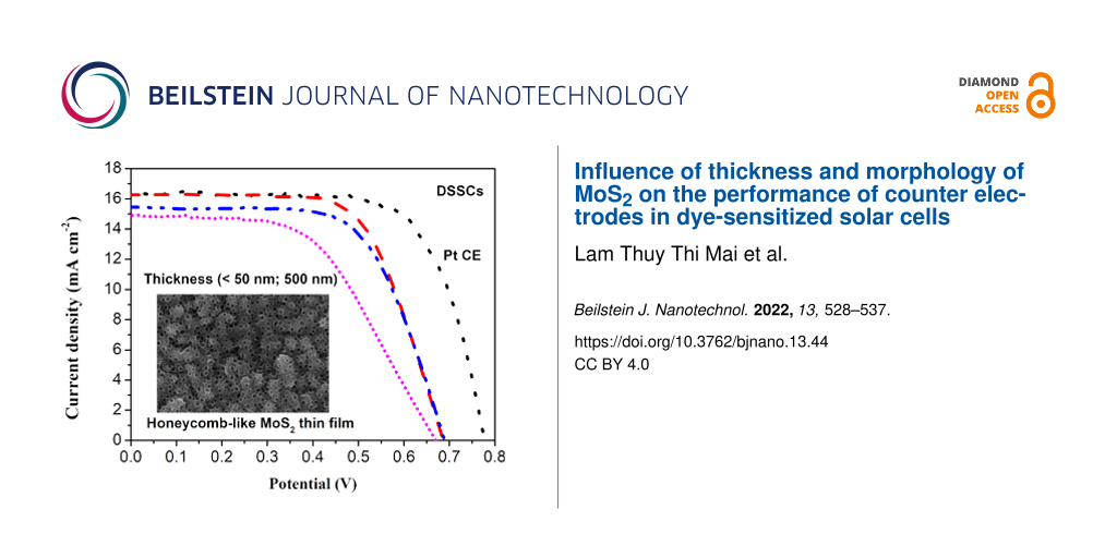
To further evaluate the effect of MoS2 morphology and thickness on the performance of the DSSCs, the photovoltaic performance of DSSCs using different MoS2 CEs was investigated under illumination. The J–V curves and the corresponding photovoltaic parameters of DSSCs are given in Figure 7 and Table 2, respectively. The DSSC using MoS2-1.25/FTO CE displayed an excellent photovoltaic performance compared to that with a Pt/FTO a CE. In particular, the obtained value of 16.3 mA·cm−2 for the short-circuit photocurrent (Jsc) was found to be higher than that of Pt/FTO CE (15.3 mA·cm−2). This is attributed to the high number of catalytically active sites together with the low resistance of this MoS2 film.
Figure 7:
Photovoltaic performance of DSSCs fabricated with different MoS2/FTO and Pt/FTO CEs.
Figure 7:
Photovoltaic performance of DSSCs fabricated with different MoS2/FTO and Pt/FTO CEs.
Although the electrocatalytic ability regarding the reduction of I3− of MoS2 was lower than that of Pt, other parameters including an open-circuit voltage (Voc) of 0.69 V, a fill factor (FF) of 0.66, and a PCE of 7.33% of this MoS2 CE-based DSSCs were comparable to those of a DSSC based on a Pt CE (VOC = 0.75 V, FF = 0.75, PEC = 8.66%) and to values found in other reports (Table 3). The PCE for DSSCs using MoS2 with different thicknesses decreased in the order: MoS2-1.25 (very thin film) > MoS2-2.5 (50 nm) > MoS2-5.0 (500 nm). This is in good agreement with the trend of Rs and Rct1 values (see Table 2 and Table 3). The effect of film thickness on the electrical conductivity of the MoS2 films was also investigated by I–V measurements (see Supporting Information File 1, Figure S2 and Table S1). The electrical conductivity of the as-prepared MoS2 decreased in the order: MoS2-1.25 (75 mS·cm−1) > MoS2-2.5 (61 mS·cm−1) > MoS2-5.0 (46 mS·cm−1). This suggests that the thickness of the MoS2 film has a significant effect on the catalytic ability and photovoltaic performance of the CE in DSSCs. Additionally, the electron lifetime (τ) indicates the recombination kinetics of electrons in the mesoscopic TiO2 film of the DSSCs. This parameter can be calculated from the peak frequency (fmax) of the low-frequency semicircles (τ = 1/2πfmax). The τ values measured under dark conditions for DSSCs devices fabricated from various CEs are presented in Table 2. The τ values for DSSCs fabricated with MoS2 CEs were higher than those of a DSSC using a Pt CE and increased in the order: DSSCs-MoS2-1.25 < DSSCs-MoS2-2.5 < DSSCs-MoS2-5.0. A longer electron lifetime indicates a slower recombination process within the DSSCs fabricated with MoS2/FTO CEs. The stability of the devices was tested by repeating the I–V measurements every week (Supporting Information File 1, Figure S3). The PCE value of a DSSC fabricated using MoS2-1.25 showed a slight decrease of 2.6% and reached stability after two weeks of testing under ambient conditions. This suggested that the MoS2-1.25/FTO CE has reversible redox activity and electrochemical stability. The electrochemical stability of the MoS2/FTO CE should provide long-term stability for solar cell devices. However, more work needs to be done to improve the efficiency of this DSSC device [36-39].
Table 3:
Performance summary of MoS2-based CEs for DSSCs.
We synthesized successfully MoS2 thin films with layered or honeycomb-like structures onto FTO substrates by the CV route. The morphology and thickness of the MoS2 films can be effectively controlled by adjusting the concentration of the precursor solution. In detail, MoS2 formed a layered thin film with a thickness of about 50 nm when the concentration level ratio between (NH4)2Mo7O24 and Na2S was 2.5/15 (solution 2.5, see Experimental section). Honeycomb MoS2 was formed with a thickness of about 500 nm from solution 5.0 (with a concentration level ratio between (NH4)2Mo7O24 and Na2S of 5/30). In addition, as-prepared MoS2 films have been used as an alternative CE to Pt in DSSCs. The short-circuit photocurrent (Jsc) was higher than that of a Pt/FTO CE. Moreover, the highest performance of solar cells was found with the layered MoS2 film thank to good electrical conductivity, a high number of catalytically active sites, and the thickness of the MoS2 film. The MoS2/FTO films could be applied as non-Pt electrodes for DSSCs in the near future.
Experimental
Materials and reagents
Ammonium molybdate tetrahydrate ((NH4)6Mo7O24·4H2O, 99.98%), sodium sulfide nonahydrate (Na2S·9H2O, 99.99%), potassium chloride (KCl, 99%), acetonitrile (ACN, CH3CN, 99%), dimethyl sulfoxide (DMSO, (CH3)2SO, 99.5%), ethanol (EtOH, CH3CH2OH, 99.8%), guanidinium thiocyanate (NH2C(=NH)NH2·HSCN, 99%), iodine (I2, 99.8%), 1-methyl-3-propylimidazolium iodide (C7H13IN2, 98%), 4-tert-butylpyridine (C9H13N, 98%), valeronitrile (CH3(CH2)3CN, 99.5%), chloroplatinic acid hexahydrate (H2PtCl6·6H2O, ≥37.50% Pt), sulfuric acid (H2SO4, 95–98%), polyvinylpyrrolidone (PVP, (C6H9NO)n, average Mw 10,000), and sodium borohydride (NaBH4, 99%) were purchased from Sigma-Aldrich (Germany). Low-temperature thermoplastic sealant (Surlyn, 25 μm), 18NR-T transparent titania paste (particle size of 20 nm), 18NR-AO active opaque titania paste (particle sizes of 20 and 450 nm), fluorine-doped tin oxide (FTO, TEC8 glass plates, 8 Ω·cm−2, 2.2 mm thickness), and N719 industry standard dye (N719) were purchased from Dyesol (Australia). All commercial chemicals were of analytical grade and were used as supplied without further purification.
Electrodeposition of MoS2 thin films
Thin films of MoS2 with different morphologies were electrodeposited onto FTO substrates by the CV method. MoS2 electrodeposition was carried out using an Autolab 302 N (Eco chemie, Netherlands) connected to a three-electrode cell. Accordingly, a Pt mesh, an Ag/AgCl (ALS, Japan), and the FTO plate (1.5 × 1.5 cm) were used as the counter electrode (CE), the reference electrode (RE), and the working electrode (WE), respectively. Prior to CV electrodeposition, the FTO substrates were first cleaned in a 1% Hellmanex solution at 70 °C for 30 min in an ultrasonic bath, then washed three times in distilled water, dried by nitrogen flow, and finally treated in a UV ozone chamber for 5 min to obtain the cleaned FTO electrode. Precursor solutions were prepared by dissolving (NH4)6Mo7O24 (x mM) and Na2S (y g·L−1) in distilled water, the pH of the solution was adjusted to 6.0 using a 20% (v/v) H2SO4 solution, KCl (0.1 M) was used as the supporting electrolyte. The concentration ratio between (NH4)2Mo7O24 and Na2S was kept constant (x/y = 1:6) with different concentration levels including 1.25:7.5 (solution 1.25), 2.5:15 (solution 2.5), and 5:30 (solution 5.0). The CV measurement was performed under a dynamic potential between −1.0 V and 1.0 V for ten cycles at a scan rate of 100 mV·s−1 in a nitrogen atmosphere.
Fabrication of DSSCs
DSSCs with an active area of 0.25 cm2 were assembled using the pre-cleaned FTO plates (1.5 × 1.5 cm) for the fabrication of anode and cathode. For cathode preparation, MoS2/FTO CEs were prepared with different morphologies from the above MoS2 samples. The obtained CEs were designated as MoS2-1.25/FTO, MoS2-2.5/FTO, and MoS2-5.0/FTO. For comparison, a Pt-based CE (Pt/FTO) was fabricated by soaking the cleaned FTO glasses in PVP–platinum suspension at 45 °C for 5 min, followed by washing with distilled water. The PVP–platinum suspension was prepared as follows: First, 1.0 g of H2PtCl6 was dissolved in 150 mL of distilled water, then 0.5 g PVP was added to the above solution under stirring for 10 min. Finally, to this solution, NaBH4 solution (1.17 g NaBH4 was dissolved in 124.8 mL of distilled water, stirred for 3 min) was added at a rate of 1.5 mL/min until the color of the mixture solution turned into black.
For the fabrication of the photoanodes, the cleaned FTO electrodes were first pretreated by immersion in a 40 mM TiCl4 solution at 70 °C for 30 min and rinsed with distilled water and ethanol. The treated FTO electrodes were then successively coated with a transparent 18NR-T titania paste (three layers) and an active opaque 18NR-AO titania paste (one outer layer) by the screen-printing method using 43T mesh. The printed electrodes were dried at room temperature for 5 min, then at 120 °C for 5 min after each printed layer, and finally heated at 450 °C under airflow for 30 min. When the temperature was cooled down to 70 °C, the electrodes were dipped in N719 dye (0.3 M N719 in the mixture DMSO/EtOH, v/v = 1:9) for 12 h to obtain the photoanodes.
For cell assembly, the DSSCs were fabricated in a nitrogen atmosphere using a glove box. Typically, the photoanode and the MoS2-based CE were sealed together by a hot-melt Surlyn film using a thermopress, pressed at 170 °C for 15 s. The electrolyte solution (0.1 M guanidinium thiocyanate, 0.03 M iodine, 1 M 1-methyl-3-propylimidazolium iodide, 0.5 M 4-tert-butylpyridine in a mixture of valeronitrile/acetonitrile with a volume ratio of 0.15:0.85) was then injected into the cell through predrilled holes on the CE. The holes were then covered with a thin glass slide using the same thermopress method as described above to obtain DSSC devices. DSSCs assembled using the CE fabricated from precursor solutions 1.25, 2.5, and 5.0 were denoted as DSSCs-MoS2-1.25, DSSCs- MoS2-2.5, and DSSCs-MoS2-5.0, respectively. For comparison, DSSCs based on Pt/FTO CE (DSSCs-Pt) were also fabricated under the same conditions.
Characterizations of MoS2 thin films
X-ray diffraction (XRD) analysis was carried out using a D8 Advance (Bruker, Germany) with a copper anode (λKα = 1.54 Å). Raman spectroscopy measurements were performed on a LabRAM HR 800 Raman Spectrometer (HORIBA Jobin Yvon) with an excitation laser source at 532 nm. The morphology of MoS2 thin films was analyzed by an ultrahigh-resolution field-emission scanning electron microscope (FE-SEM, Hitachi SU-8010, Japan). The electrochemical catalytic activity of the MoS2-based CEs was studied regarding the I3−/I− redox couple (prepared with 10 mM I2, 20 mM KI, and 0.1 M LiClO4 in acetonitrile) and compared to that of a FTO/Pt CE by CV.
DSSC characterizations
Photoelectrochemical measurements were performed using an Oriel Sol1A class ABB solar simulator (Oriel-Newport-USA, Model No. 94061A). Simulated sunlight of 100 mW·cm−2 (1 sun) was generated and corrected by a 1000 W Xe lamp and an AM 1.5 filter. The photocurrent density–voltage (J–V) curves of the DSSCs were measured using a Keithley model 2400 multisource meter. Electrochemical impedance spectroscopy (EIS) of the fabricated DSSCs was carried out using an Autolab 302 N equipped with a FRA 32M module. The EIS measurements were carried out at open-circuit voltage with an alternating voltage amplitude of 10 mV under dark conditions in a frequency range between 0.01 Hz and 100 kHz. The efficiency of the DSSCs was analyzed and reported as the average of three cells.
Supporting Information
Supporting Information File 1:
Additional experimental data.
We thank Professor Tzu-Chien Wei, Department of Chemical Engineering, National Tsing Hua University, Taiwan, for his great help on EIS, AFM and Raman measurements.
Funding
This research was fully funded by Tra Vinh University under grant contract number 140/HĐ.HĐKH-ĐHTV
References
Vikraman, D.; Patil, S. A.; Hussain, S.; Mengal, N.; Kim, H.-S.; Jeong, S. H.; Jung, J.; Kim, H.-S.; Park, H. J. Dyes Pigm.2018,151, 7–14. doi:10.1016/j.dyepig.2017.12.037
Return to citation in text:
[1]
[2]
[3]
[4]
[5]
Roy-Mayhew, J. D.; Bozym, D. J.; Punckt, C.; Aksay, I. A. ACS Nano2010,4, 6203–6211. doi:10.1021/nn1016428
Return to citation in text:
[1]
[2]
Chen, J.; Li, K.; Luo, Y.; Guo, X.; Li, D.; Deng, M.; Huang, S.; Meng, Q. Carbon2009,47, 2704–2708. doi:10.1016/j.carbon.2009.05.028
Return to citation in text:
[1]
Yang, Z.; Chen, T.; He, R.; Guan, G.; Li, H.; Qiu, L.; Peng, H. Adv. Mater. (Weinheim, Ger.)2011,23, 5436–5439. doi:10.1002/adma.201103509
Return to citation in text:
[1]
Lee, K. S.; Lee, H. K.; Wang, D. H.; Park, N. G.; Lee, J. Y.; Park, O. O.; Park, J. H. Chem. Commun.2010,46, 4505–4507. doi:10.1039/c0cc00432d
Return to citation in text:
[1]
[2]
Li, C.-T.; Lee, C.-P.; Li, Y.-Y.; Yeh, M.-H.; Ho, K.-C. J. Mater. Chem. A2013,1, 14888–14896. doi:10.1039/c3ta12603j
Return to citation in text:
[1]
[2]
Wu, M.; Wang, Y.; Lin, X.; Yu, N.; Wang, L.; Wang, L.; Hagfeldt, A.; Ma, T. Phys. Chem. Chem. Phys.2011,13, 19298–19301. doi:10.1039/c1cp22819f
Return to citation in text:
[1]
[2]
Liu, C.-J.; Tai, S.-Y.; Chou, S.-W.; Yu, Y.-C.; Chang, K.-D.; Wang, S.; Chien, F. S.-S.; Lin, J.-Y.; Lin, T.-W. J. Mater. Chem.2012,22, 21057–21064. doi:10.1039/c2jm33679k
Return to citation in text:
[1]
[2]
Hussain, S.; Shaikh, S. F.; Vikraman, D.; Mane, R. S.; Joo, O.-S.; Naushad, M.; Jung, J. ChemPhysChem2015,16, 3959–3965. doi:10.1002/cphc.201500644
Return to citation in text:
[1]
[2]
[3]
Al-Mamun, M.; Zhang, H.; Liu, P.; Wang, Y.; Cao, J.; Zhao, H. RSC Adv.2014,4, 21277–21283. doi:10.1039/c4ra00583j
Return to citation in text:
[1]
[2]
[3]
Wei, W.; Sun, K.; Hu, Y. H. J. Mater. Chem. A2016,4, 12398–12401. doi:10.1039/c6ta04743b
Return to citation in text:
[1]
[2]
[3]
[4]
[5]
Liang, J.; Li, J.; Zhu, H.; Han, Y.; Wang, Y.; Wang, C.; Jin, Z.; Zhang, G.; Liu, J. Nanoscale2016,8, 16017–16025. doi:10.1039/c6nr03635j
Return to citation in text:
[1]
[2]
[3]
Liu, W.; He, S.; Yang, T.; Feng, Y.; Qian, G.; Xu, J.; Miao, S. Appl. Surf. Sci.2014,313, 498–503. doi:10.1016/j.apsusc.2014.06.011
Return to citation in text:
[1]
[2]
[3]
[4]
Patil, S. A.; Kalode, P. Y.; Mane, R. S.; Shinde, D. V.; Doyoung, A.; Keumnam, C.; Sung, M. M.; Ambade, S. B.; Han, S.-H. Dalton Trans.2014,43, 5256–5259. doi:10.1039/c3dt53356e
Return to citation in text:
[1]
[2]
[3]
Lei, B.; Li, G. R.; Gao, X. P. J. Mater. Chem. A2014,2, 3919–3925. doi:10.1039/c3ta14313a
Return to citation in text:
[1]
[2]
[3]
[4]
Liu, Z.; Gao, Z.; Liu, Y.; Xia, M.; Wang, R.; Li, N. ACS Appl. Mater. Interfaces2017,9, 25291–25297. doi:10.1021/acsami.7b05775
Return to citation in text:
[1]
[2]
Li, G.; Zhang, D.; Qiao, Q.; Yu, Y.; Peterson, D.; Zafar, A.; Kumar, R.; Curtarolo, S.; Hunte, F.; Shannon, S.; Zhu, Y.; Yang, W.; Cao, L. J. Am. Chem. Soc.2016,138, 16632–16638. doi:10.1021/jacs.6b05940
Return to citation in text:
[1]
Jaramillo, T. F.; Jørgensen, K. P.; Bonde, J.; Nielsen, J. H.; Horch, S.; Chorkendorff, I. Science2007,317, 100–102. doi:10.1126/science.1141483
Return to citation in text:
[1]
Aliyev, A. S.; Elrouby, M.; Cafarova, S. F. Mater. Sci. Semicond. Process.2015,32, 31–39. doi:10.1016/j.mssp.2015.01.006
Return to citation in text:
[1]
Li, S.; Min, H.; Xu, F.; Tong, L.; Chen, J.; Zhu, C.; Sun, L. RSC Adv.2016,6, 34546–34552. doi:10.1039/c6ra02494g
Return to citation in text:
[1]
Quy, V. H. V.; Vijayakumar, E.; Ho, P.; Park, J.-H.; Rajesh, J. A.; Kwon, J.; Chae, J.; Kim, J.-H.; Kang, S.-H.; Ahn, K.-S. Electrochim. Acta2018,260, 716–725. doi:10.1016/j.electacta.2017.12.023
Return to citation in text:
[1]
[2]
[3]
Gurulakshmi, M.; Meenakshamma, A.; Siddeswaramma, G.; Susmitha, K.; Venkata Subbaiah, Y. P.; Narayana, T.; Raghavender, M. Sol. Energy2020,199, 447–452. doi:10.1016/j.solener.2020.02.047
Return to citation in text:
[1]
[2]
Chang, C.-Y.; Anuratha, K. S.; Lin, Y.-H.; Xiao, Y.; Hasin, P.; Lin, J.-Y. Sol. Energy2020,206, 163–170. doi:10.1016/j.solener.2020.06.001
Return to citation in text:
[1]
[2]
[3]
[4]
[5]
Ghayad, I. M.; Al Kharafi, F. M.; Saad, A. Y.; Ateya, B. G. Mod. Appl. Sci.2010,4, 2–11. doi:10.5539/mas.v4n3p2
Return to citation in text:
[1]
Wang, L.; Lu, P.; Liu, C.; Wang, L. Int. J. Electrochem. Sci.2015,10, 8374–8384.
Return to citation in text:
[1]
Falola, B. D.; Wiltowski, T.; Suni, I. I. J. Electrochem. Soc.2016,163, D568–D574. doi:10.1149/2.0011610jes
Return to citation in text:
[1]
[2]
[3]
[4]
Ponomarev, E. A.; Neumann-Spallart, M.; Hodes, G.; Lévy-Clément, C. Thin Solid Films1996,280, 86–89. doi:10.1016/0040-6090(95)08204-2
Return to citation in text:
[1]
Ghosh, S. K.; Bera, T.; Karacasu, O.; Swarnakar, A.; Buijnsters, J. G.; Celis, J. P. Electrochim. Acta2011,56, 2433–2442. doi:10.1016/j.electacta.2010.10.065
Return to citation in text:
[1]
Tan, S. J. R.; Sarkar, S.; Zhao, X.; Luo, X.; Luo, Y. Z.; Poh, S. M.; Abdelwahab, I.; Zhou, W.; Venkatesan, T.; Chen, W.; Quek, S. Y.; Loh, K. P. ACS Nano2018,12, 5051–5058. doi:10.1021/acsnano.8b02649
Return to citation in text:
[1]
Sharma, C. H.; Surendran, A. P.; Varghese, A.; Thalakulam, M. Sci. Rep.2018,8, 12463. doi:10.1038/s41598-018-30867-y
Return to citation in text:
[1]
Nayak, A. P.; Pandey, T.; Voiry, D.; Liu, J.; Moran, S. T.; Sharma, A.; Tan, C.; Chen, C.-H.; Li, L.-J.; Chhowalla, M.; Lin, J.-F.; Singh, A. K.; Akinwande, D. Nano Lett.2015,15, 346–353. doi:10.1021/nl5036397
Return to citation in text:
[1]
Windom, B. C.; Sawyer, W. G.; Hahn, D. W. Tribol. Lett.2011,42, 301–310. doi:10.1007/s11249-011-9774-x
Return to citation in text:
[1]
Blanco, É.; Afanasiev, P.; Berhault, G.; Uzio, D.; Loridant, S. C. R. Chim.2016,19, 1310–1314. doi:10.1016/j.crci.2015.08.014
Return to citation in text:
[1]
[2]
[3]
Rashidi, S.; Rashidi, S.; Heydari, R. K.; Esmaeili, S.; Tran, N.; Thangi, D.; Wei, W. Prog. Photovoltaics2021,29, 238–261. doi:10.1002/pip.3350
Return to citation in text:
[1]
Akman, E.; Akin, S.; Ozturk, T.; Gulveren, B.; Sonmezoglu, S. Sol. Energy2020,202, 227–237. doi:10.1016/j.solener.2020.03.108
Return to citation in text:
[1]
Vikraman, D.; Patil, S. A.; Hussain, S.; Mengal, N.; Kim, H.-S.; Jeong, S. H.; Jung, J.; Kim, H.-S.; Park, H. J. Dyes Pigm.2018,151, 7–14. doi:10.1016/j.dyepig.2017.12.037
Vikraman, D.; Patil, S. A.; Hussain, S.; Mengal, N.; Kim, H.-S.; Jeong, S. H.; Jung, J.; Kim, H.-S.; Park, H. J. Dyes Pigm.2018,151, 7–14. doi:10.1016/j.dyepig.2017.12.037
Patil, S. A.; Kalode, P. Y.; Mane, R. S.; Shinde, D. V.; Doyoung, A.; Keumnam, C.; Sung, M. M.; Ambade, S. B.; Han, S.-H. Dalton Trans.2014,43, 5256–5259. doi:10.1039/c3dt53356e
Patil, S. A.; Kalode, P. Y.; Mane, R. S.; Shinde, D. V.; Doyoung, A.; Keumnam, C.; Sung, M. M.; Ambade, S. B.; Han, S.-H. Dalton Trans.2014,43, 5256–5259. doi:10.1039/c3dt53356e
Patil, S. A.; Kalode, P. Y.; Mane, R. S.; Shinde, D. V.; Doyoung, A.; Keumnam, C.; Sung, M. M.; Ambade, S. B.; Han, S.-H. Dalton Trans.2014,43, 5256–5259. doi:10.1039/c3dt53356e
Vikraman, D.; Patil, S. A.; Hussain, S.; Mengal, N.; Kim, H.-S.; Jeong, S. H.; Jung, J.; Kim, H.-S.; Park, H. J. Dyes Pigm.2018,151, 7–14. doi:10.1016/j.dyepig.2017.12.037
Vikraman, D.; Patil, S. A.; Hussain, S.; Mengal, N.; Kim, H.-S.; Jeong, S. H.; Jung, J.; Kim, H.-S.; Park, H. J. Dyes Pigm.2018,151, 7–14. doi:10.1016/j.dyepig.2017.12.037
Vikraman, D.; Patil, S. A.; Hussain, S.; Mengal, N.; Kim, H.-S.; Jeong, S. H.; Jung, J.; Kim, H.-S.; Park, H. J. Dyes Pigm.2018,151, 7–14. doi:10.1016/j.dyepig.2017.12.037
17.
Liu, Z.; Gao, Z.; Liu, Y.; Xia, M.; Wang, R.; Li, N. ACS Appl. Mater. Interfaces2017,9, 25291–25297. doi:10.1021/acsami.7b05775
36.
Blanco, É.; Afanasiev, P.; Berhault, G.; Uzio, D.; Loridant, S. C. R. Chim.2016,19, 1310–1314. doi:10.1016/j.crci.2015.08.014
Tan, S. J. R.; Sarkar, S.; Zhao, X.; Luo, X.; Luo, Y. Z.; Poh, S. M.; Abdelwahab, I.; Zhou, W.; Venkatesan, T.; Chen, W.; Quek, S. Y.; Loh, K. P. ACS Nano2018,12, 5051–5058. doi:10.1021/acsnano.8b02649
Falola, B. D.; Wiltowski, T.; Suni, I. I. J. Electrochem. Soc.2016,163, D568–D574. doi:10.1149/2.0011610jes
29.
Ponomarev, E. A.; Neumann-Spallart, M.; Hodes, G.; Lévy-Clément, C. Thin Solid Films1996,280, 86–89. doi:10.1016/0040-6090(95)08204-2
30.
Ghosh, S. K.; Bera, T.; Karacasu, O.; Swarnakar, A.; Buijnsters, J. G.; Celis, J. P. Electrochim. Acta2011,56, 2433–2442. doi:10.1016/j.electacta.2010.10.065


![[2190-4286-13-44-i1]](/bjnano/content/inline/2190-4286-13-44-i1.svg?max-width=590&scale=1.18182)
![[2190-4286-13-44-i2]](/bjnano/content/inline/2190-4286-13-44-i2.svg?max-width=590&scale=1.18182)
![[2190-4286-13-44-i3]](/bjnano/content/inline/2190-4286-13-44-i3.svg?max-width=590&scale=1.18182)
![[2190-4286-13-44-i4]](/bjnano/content/inline/2190-4286-13-44-i4.svg?max-width=590&scale=1.18182)
![[2190-4286-13-44-i5]](/bjnano/content/inline/2190-4286-13-44-i5.svg?max-width=590&scale=1.18182)
![[2190-4286-13-44-1]](/bjnano/content/figures/2190-4286-13-44-1.png?scale=2.0&max-width=1024&background=FFFFFF)
![[2190-4286-13-44-2]](/bjnano/content/figures/2190-4286-13-44-2.png?scale=2.0&max-width=1024&background=FFFFFF)
![[2190-4286-13-44-3]](/bjnano/content/figures/2190-4286-13-44-3.png?scale=2.0&max-width=1024&background=FFFFFF)
![[2190-4286-13-44-4]](/bjnano/content/figures/2190-4286-13-44-4.png?scale=2.0&max-width=1024&background=FFFFFF)
![[2190-4286-13-44-5]](/bjnano/content/figures/2190-4286-13-44-5.png?scale=2.0&max-width=1024&background=FFFFFF)
![[2190-4286-13-44-6]](/bjnano/content/figures/2190-4286-13-44-6.png?scale=2.0&max-width=1024&background=FFFFFF)
![[2190-4286-13-44-7]](/bjnano/content/figures/2190-4286-13-44-7.png?scale=2.0&max-width=1024&background=FFFFFF)