Abstract
This work presents results of the optical and structural characterization of oleic acid-stabilized cadmium telluride nanocrystals (CdTe-NC) synthesized by an organometallic route. After being cleaned, the CdTe-NC were dispersed in toluene to obtain an ink-like dispersion, which was drop-cast on glass substrate to deposit a thin film. The CdTe-NC colloidal dispersion as well as the CdTe drop-cast thin films were characterized with regard to the optical and structural properties. TEM analysis indicates that the CdTe-NC have a nearly spherical shape (3.5 nm as mean size). Electron diffraction and XRD diffraction analyses indicated the bulk-CdTe face-centered cubic structure for CdTe-NC. An additional diffraction line corresponding to the octahedral Cd3P2 was also detected as a secondary phase, which probably originates by reacting free cadmium ions with trioctylphosphine (the tellurium reducing agent). The Raman spectrum exhibits two broad bands centered at 141.6 and 162.3 cm−1, which could be associated to the TO and LO modes of cubic CdTe nanocrystals, respectively. Additional peaks located in the 222 to 324 cm−1 range, agree fairly well with the wavenumbers reported for TO modes of octahedral Cd3P2.
Introduction
Currently colloidal chemistry is a promising technique in materials science research due to its simplicity, low cost, and its capability to process nearly-monodisperse nanocrystals of a variety of semiconductor materials at low temperatures and using non sophisticated equipments [1,2]. It has been extensively used to prepare binary [3-5], ternary [6-8] and quaternary [9,10] semiconductors for applications in quantum effect based devices [11] such as light emitting diodes [12], biolabeling [13], thermoelectric generators [14] and thin film solar cells [15]. In solar cell technology, colloidal nanocrystals hold promise for producing cheap solar cells with improved conversion efficiency by using quantum effects such as multiple exciton generation [16]. In the last years, nanostructured semiconductors have proved to be useful as raw material for solution-processable electronic technologies. The capping of semiconductor nanocrystals by organic ligands, provides the control of composition, size, shape and crystal structure, which make them very attractive in this technological area. Thin films deposition techniques such as drop-casting [17], screen printing [18], and ink jet printing [19], are currently used to fabricate electronic devices on great variety of substrates, either rigid or flexible, looking for preserve their size effects [20-22]. All of these techniques need ink-like stable dispersions comprising functionalized nanomaterials dispersed in a convenient solvent. Drop-casting offers a cost efficient production of photovoltaic semiconductor thin films. Nevertheless, depending on the dispersion chemistry and on the required thin film optoelectronic properties, post-deposition complex processes are needed. Guo et al. [23] deposited CuInSe2 (CIS) thin films for solar cells starting from oleylamine-stabilized CIS nanocrystals. An additional annealing at 500 °C was needed to obtain suitable CIS films for photovoltaic applications. Jasieniak et al. [24] deposited photovoltaic cadmium telluride (CdTe) thin films by using pyridine-capped CdTe nanocrystals. In their approach, CdTe nanocrystals were deposited from solution by a layer-by-layer process with subsequent annealing per layer at 300, 350 and 400 °C. On the other hand, oleic acid is a green organic ligand, which has been successfully used in preparing a great variety of colloidal materials [15,25,26], including CdTe quantum dots [27-29].
This work presents our early results on the elaboration of CdTe-based inks for potential uses in solution-processable thin film solar cells. The CdTe-NC were prepared by colloidal chemistry using an organic–inorganic reaction [30]. The product comprised toluene-dispersed oleic acid-stabilized CdTe-NC and cadmium phosphide (Cd3P2) as a secondary phase. Oleic acid was chosen because it enabled us to manipulate the CdTe nanocrystals under ambient conditions, and to use them to deposit CdTe thin films that were free of cadmium tellurate or tellurium oxide. The CdTe nanocrystals and thin films were characterized by TEM, X-ray diffraction, UV–vis spectroscopy and Raman spectroscopy.
Results and Discussion
TEM analysis
In general, well crystallized CdTe colloids were obtained, as shown in Figure 1b. We were unable to assess the size and shape of the samples. Although the absorbance spectrum displays a sharp excitonic peak indicating a nearly monodispersed nature of our samples, the degree of monodispersity could not be evaluated from the TEM micrograph. The TEM image of Figure 1a shows CdTe-NC with a size of 3.5 nm, the electron diffraction pattern (inset Figure 1a), indicated the face-centered cubic phase for CdTe as reported by Talapin et al. [31]. The electron diffraction pattern was indexed following the method reported elsewhere [32]. In addition, an extra phase was disclosed; it was attributed to the Cd3P2 impurity phase, which crystalizes in the octahedral structure. The above described features could be corroborated by XRD and Raman spectroscopy (see below).
![[2190-4286-5-100-1]](/bjnano/content/figures/2190-4286-5-100-1.jpg?scale=2.0&max-width=1024&background=FFFFFF)
Figure 1: a) TEM micrograph of CdTe nanocrystals, the inset shows the indexed electron diffraction pattern, b) TEM image of CdTe nanocrystals used to determinate the lattice parameter. The inset shows the 3.23 Å (200) lattice parameter.
Figure 1: a) TEM micrograph of CdTe nanocrystals, the inset shows the indexed electron diffraction pattern, b...
Figure 2 shows a CdTe deposition with and without UV illumination. We further note that the nanocrystal luminescence under ambient conditions is preserved.
![[2190-4286-5-100-2]](/bjnano/content/figures/2190-4286-5-100-2.png?scale=2.0&max-width=1024&background=FFFFFF)
Figure 2: CdTe deposition with and without UV illumination under ambient conditions.
Figure 2: CdTe deposition with and without UV illumination under ambient conditions.
X-ray diffraction analysis
The structural properties of the prepared samples were evaluated by XRD and Raman spectroscopy, using CdTe thin films deposited on glass substrates (see Figure 2). As mentioned above, XRD and Raman measurements corroborated the phase composition of the colloids. Figure 3 shows the X-ray diffraction patterns of deposited CdTe-NC at concentrations of 2.24 and 0.45 mmol trioctylphosphine (TOP), respectively. The diffraction patterns display the typical low intensity and broad peaks of a nanosized material. The peaks at 23.7, 39.3 and 46.6°, could be ascribed to (111), (220) and (311) diffraction lines of the face-centered cubic structure of CdTe [33,34]. The narrow peak at 29.5° appearing at a concentration of 2.24 mmol TOP could be attributed to the octahedral phase of Cd3P2 [35], so testifying the electron diffraction results. It is also observed that Cd3P2 disappeared at the low TOP concentration (Figure 3). The crystal size, as determinated by using the Debye–Scherrer formula, was 3.7 nm, which is in good agreement with the value ascertained by TEM. The Debye–Scherrer formula is [36]:
![[Graphic 1]](/bjnano/content/inline/2190-4286-5-100-i1.svg?max-width=637&scale=1.18182)
where K is the Scherrer constant, taken as 0.9 for cubic crystal structures, λ is the X-ray wavelength, Δ is the full width at half maximum (FWHM) of the diffraction peak and θ is the Bragg angle.
![[2190-4286-5-100-3]](/bjnano/content/figures/2190-4286-5-100-3.png?scale=2.0&max-width=1024&background=FFFFFF)
Figure 3: X-ray diffraction pattern of deposited CdTe nanocrystals.
Figure 3: X-ray diffraction pattern of deposited CdTe nanocrystals.
Raman spectroscopy
Raman spectroscopy is a valuable technique to assess the structure of semiconductors also at the nanometer-scale. In particular, Raman spectroscopy is sensitive to size effects, because like the excitons, phonons experience quantum confinement effects depending on the crystal size. In CdTe, the quantum confinement effect is revealed by the broadening and red shifting of the LO mode [37]. Figure 4 shows the cubic CdTe Raman peaks at 142 and 162.3 cm−1 corresponding to TO and LO modes [38], respectively. It is seen that, the LO mode red-shifts by 5.7 cm−1 with respect to bulk CdTe [38]. On the other hand, all Raman peaks in the range between 200 and 350 cm−1 belong to octahedral Cd3P2 [35], as previously stated by TEM and XRD.
![[2190-4286-5-100-4]](/bjnano/content/figures/2190-4286-5-100-4.png?scale=2.0&max-width=1024&background=FFFFFF)
Figure 4: Raman spectrum of drop-cast CdTe nanocrystals measured with a 632 nm He–Ne laser.
Figure 4: Raman spectrum of drop-cast CdTe nanocrystals measured with a 632 nm He–Ne laser.
In addition, we have used the Richter–Wang–Law model [37,39], to calculate the crystallite size by fitting the LO peak. The obtained value was 3.4 nm, which is in good agreement with that calculated by TEM and XRD. Interestingly, the CdTe crystallites preserve their size when deposited in the glass substrate, so testifying the suitable oleic acid stabilization. In regarding the Cd3P2 formation, it is thought that it was originated by reacting cadmium and phosphor ions, with the latter being provided by the TOP decomposition. Because as reported by Chen et al. [40] and Henkes et al. [41], the high reactivity of transition metals promotes the P–C cleavage and the release of the phosphor ions. Surprisingly, the Cd3P2 formation depends on the TOP concentration, because as indicated in Figure 3, for TOP concentration lower than 2.4 mmol, impurity-free CdTe colloids were obtained.
Optical characterization
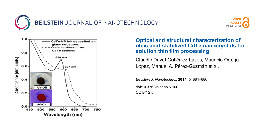
According to Figure 2, our CdTe colloids display a strong red luminescence, indicating quantum confinement in the nanosized CdTe crystals. It is known that quantum confinement can be observed for crystallite sizes lower than the exciton Bohr radius of the bulk counterpart. In the case of CdTe, the reported parameter is 6.8 nm [42], whilst the CdTe crystal size was 3.5 nm, as estimated from TEM and XRD measurements. The absorbance spectra shown in Figure 5 exhibit a well-defined peak in the visible wavelength range. This peak corresponds to the band-to-band transition, since it is the most likely transition under the quantum confinement regime [43]. It is worthy to note that CdTe nanocrystals dispersed in toluene showed a narrow absorption peak (or excitonic peak) around 590 nm, suggesting a narrow size distribution for our samples. Nevertheless the exciton peak disappeared once the CdTe colloid was drop-cast on the glass substrates Figure 5 shows the absorbance spectra of CdTe-NC of the colloidal solution and of a liquid sample processed by the size-separation technique. The effect of size-separation can be observed by considering the maximum absorption peak. The excitonic peak is narrower than that the of the colloid and nearly symmetric, similar to a nearly monodispersed sample. Additionally, the maximum absorbance has shifted from 607 nm to 589 nm arguing for a lower size dispersion of the CdTe-NC. However, this result imposes a technological limitation in the colloid application in a thin-film device due to strong stabilization of oleic acid, which is nonconductive and separates the nanocrystals with spacings of about 0.7 nm and thus impedes their electrical contact [15].
![[2190-4286-5-100-5]](/bjnano/content/figures/2190-4286-5-100-5.png?scale=2.0&max-width=1024&background=FFFFFF)
Figure 5: Absorbance spectra of the colloidal solution and CdTe-NC processed by size-separation and re-dispersed in toluene.
Figure 5: Absorbance spectra of the colloidal solution and CdTe-NC processed by size-separation and re-disper...
Conclusion
Oleic acid-stabilized CdTe nanocrystals were prepared by colloidal chemistry. A toluene dispersible product comprising CdTe and Cd3P2 as impurity was obtained. The ink-like dispersion was successfully to deposit thin films on glass substrate. It was demonstrated that the phase composition depends strongly on the TOP concentration, TOP concentration lower than 2.24 mmol produced free Cd3P2 CdTe colloids.
Experimental
Materials: cadmium oxide powder ≈1 μm (CdO, 99.5% Aldrich); tellurium powder (200 mesh 99.8% Aldrich); oleic acid (OA, technical grade 90% Aldrich); n-trioctylphosphine (TOP, technical grade 90% Aldrich); 1-octadecene (1-ODC, technical grade 90% Aldrich).
Synthesis of CdTe nanocrystals: Colloidal CdTe-NCs were synthesized via an organic–inorganic route using oleic acid as the stabilizer and 1-octadecene as the solvent. The tellurium precursor was prepared by dissolving tellurium powder (12.8 mg, 0.1 mmol) in a previously prepared 1-octadecene (4 mL)/TOP (1 mL, 2.24 mmol or 0.2 mL, 0.45 mmol) mixture. The solution was heated to 120 °C for 15 min, under N2 atmosphere and vigorous magnetic stirring. The TOP–Te solution was maintained under inert atmosphere until its use. Cadmium oleate was used as cadmium precursor, which was prepared also under N2 atmosphere by mixing 25.6 mg (0.2 mmol) of cadmium oxide and 0.5 mL (0.315 mmol) of oleic acid in 10 mL of 1-octadecene. Reagents were mixed with vigorous magnetic stirring at 210 °C until the complete dissolution of CdO powder. Subsequently, the TOP–Te solution was transferred through flexible tubing by using N2 flux and the colloid temperature was reduced to 190 ± 2 °C. This value was maintained as reflux temperature.
Sample preparation to optical and structural characterization: Initially, the CdTe-NC were processed by a size separation technique. On a colloidal solution, ethanol aliquots were dropped and the flocculated solid phase was removed from solution, rinsed also with ethanol and dried with N2. This process was repeated until the solid phase remained completely attached to the flask bottom. Finally, nanocrystals were dispersed with 2–4 mL toluene and deposited on glass substrates via drop-casting technique without annealing. For absorbance characterization, a liquid sample processed by the size-separation technique was analyzed and for Raman measurements, the same sample but deposited by dripping on glass substrate was studied.
TEM characterization: Shape, size and crystal structure of CdTe-NC were determined by transmission electron microscopy (TEM) using a JEOL 2010 microscope. For TEM characterization, the nanocrystals solution were dropped on 300 mesh Lacey carbon grid and dried under laboratory conditions. X-ray diffraction (XRD) measurements were done on depositions by using a Bruker AXs D8 Discover diffractometer at normal incidence, using Cu Kα radiation (λ = 0.1506 nm). Absorbance of CdTe colloids and CdTe nanocrystals re-dispersed in toluene were carried out at room temperature by using a Shimadzu 2401 UV–vis spectrophotometer. Raman spectroscopy was carried out also on drop-cast samples by using a Horiba Jobin-Yvon system with an Olympus BX40 microscope, employing the 632 nm He–Ne laser wavelength.
Acknowledgements
The authors are very thankful to Consejo Nacional de Ciencia y Tecnología (CONACyT-México) by its sponsorship under the grant “2do año de Continuidad de Estancias Posdoctorales Vinculadas al Fortalecimiento de la Calidad del Posgrado Nacional 2013 (2)”. Also, authors are very thankful to Dr. Jaime Santoyo Salazar at the TEM facilities, Álvaro Guzmán Campuzano for his technical assistance in the nanocrystal synthesis, and M. Sc. Alejandra García Sotelo for the Raman measurements.
References
-
Murray, C. B.; Norris, D. J.; Bawendi, M. G. J. Am. Chem. Soc. 1993, 115, 8706–8715. doi:10.1021/ja00072a025
Return to citation in text: [1] -
Murray, C. B.; Kagan, C. R.; Bawendi, M. G. Annu. Rev. Mater. Sci. 2000, 30, 545–610. doi:10.1146/annurev.matsci.30.1.545
Return to citation in text: [1] -
Rogach, A. L.; Franzl, T.; Klar, T. A.; Feldmann, J.; Gaponik, N.; Lesnyak, V.; Shavel, A.; Eychmüller, A.; Rakovich, Y. P.; Donegan, J. F. J. Phys. Chem. C 2007, 111, 14628–14637. doi:10.1021/jp072463y
Return to citation in text: [1] -
Winter, J. O.; Gomez, N.; Gatzert, S.; Schmidt, C. E.; Korgel, B. A. Colloids Surf., A 2005, 254, 147–157. doi:10.1016/j.colsurfa.2004.11.024
Return to citation in text: [1] -
Kumar, A.; Singhal, A. Nanotechnology 2007, 18, 475703. doi:10.1088/0957-4484/18/47/475703
Return to citation in text: [1] -
Castro, S. L.; Bailey, S. G.; Raffaelle, R. P.; Banger, K. K.; Hepp, A. F. J. Phys. Chem. B 2004, 108, 12429–12435. doi:10.1021/jp049107p
Return to citation in text: [1] -
Protière, M.; Reiss, P. Small 2007, 3, 399–403. doi:10.1002/smll.200600581
Return to citation in text: [1] -
Zhong, X.; Feng, Y.; Knoll, W.; Han, M. J. Am. Chem. Soc. 2003, 125, 13559–13563. doi:10.1021/ja036683a
Return to citation in text: [1] -
Shavel, A.; Arbiol, J.; Cabot, A. J. Am. Chem. Soc. 2010, 132, 4514–4515. doi:10.1021/ja909498c
Return to citation in text: [1] -
Guo, Q.; Hillhouse, H. W.; Agrawal, R. J. Am. Chem. Soc. 2009, 131, 11672–11673. doi:10.1021/ja904981r
Return to citation in text: [1] -
Talapin, D. V.; Lee, J.-S.; Kovalenko, M. V.; Shevchenko, E. V. Chem. Rev. 2010, 110, 389–458. doi:10.1021/cr900137k
Return to citation in text: [1] -
Bertoni, C.; Gallardo, D.; Dunn, S.; Gaponik, N.; Eychmüller, A. Appl. Phys. Lett. 2007, 90, 034107. doi:10.1063/1.2433030
Return to citation in text: [1] -
Mamedova, N. N.; Kotov, N. A.; Rogach, A. L.; Studer, J. Nano Lett. 2001, 1, 281–286. doi:10.1021/nl015519n
Return to citation in text: [1] -
Lu, W. G.; Fang, J. Y.; Stokes, K. L.; Lin, J. J. Am. Chem. Soc. 2004, 126, 11798–11799. doi:10.1021/ja0469131
Return to citation in text: [1] -
Tang, J.; Kemp, K. W.; Hoogland, S.; Jeong, K. S.; Liu, H.; Levina, L.; Furukawa, M.; Wang, X.; Debnath, R.; Cha, D.; Chou, K. W.; Fischer, A.; Amassian, A.; Asbury, J. B.; Sargent, E. H. Nat. Mater. 2011, 10, 765–771. doi:10.1038/nmat3118
Return to citation in text: [1] [2] [3] -
Luque, J. A.; Martí, A.; Nozik, A. J. MRS Bull. 2007, 32, 236–241. doi:10.1557/mrs2007.28
Return to citation in text: [1] -
Peng, S.; Zhang, S.; Mhaisalkar, S. G.; Ramakrishna, S. Phys. Chem. Chem. Phys. 2012, 14, 8523–8529. doi:10.1039/c2cp40848a
Return to citation in text: [1] -
ul Hasan, K.; Nur, O.; Willander, M. Appl. Phys. Lett. 2012, 100, 211104. doi:10.1063/1.4720179
Return to citation in text: [1] -
Tekin, E.; Smith, P. J.; Hoeppener, S.; van den Berg, A. M. J.; Susha, A. S.; Rogach, A. L.; Feldmann, J.; Schubert, U. S. Adv. Funct. Mater. 2007, 17, 23–28. doi:10.1002/adfm.200600587
Return to citation in text: [1] -
Chen, L.; Yang, H.; Qiang, Z.; Pang, H.; Sun, L.; Ma, Z.; Pate, R.; Stiff-Roberts, A.; Gao, S.; Xu, J.; Brown, G. J.; Zhou, W. Appl. Phys. Lett. 2010, 96, 083111. doi:10.1063/1.3337095
Return to citation in text: [1] -
Urban, J. J.; Talapin, D. V.; Shevchenko, E. V.; Murray, C. B. J. Am. Chem. Soc. 2006, 128, 3248–3255. doi:10.1021/ja058269b
Return to citation in text: [1] -
Hasan, S. A.; Kavich, D. W.; Mahajan, S. V.; Dickerson, J. H. Thin Solid Films 2009, 517, 2665–2669. doi:10.1016/j.tsf.2008.10.122
Return to citation in text: [1] -
Guo, Q.; Kim, S. J.; Kar, M.; Shafarman, W. N.; Birkmire, R. W.; Stach, E. A.; Agrawal, R.; Hillhouse, H. W. Nano Lett. 2008, 8, 2982–2987. doi:10.1021/nl802042g
Return to citation in text: [1] -
Jasieniak, J.; MacDonald, B. I.; Watkins, S. E.; Mulvaney, P. Nano Lett. 2011, 11, 2856–2864. doi:10.1021/nl201282v
Return to citation in text: [1] -
Sun, X.; Dai, R.; Chen, J.; Zhou, W.; Wang, T.; Kost, A. R.; Tsung, C. K.; An, Z. Opt. Express 2014, 22, 519–524. doi:10.1364/OE.22.000519
Return to citation in text: [1] -
de la Presa, P.; Multigner, M.; de la Venta, J.; García, M. A.; Ruiz-González, M. L. J. Appl. Phys. 2006, 100, 123915. doi:10.1063/1.2401314
Return to citation in text: [1] -
Vasiliev, R. B.; Vinogradov, V. S.; Dorofeev, S. G.; Kozyrev, S. P.; Kucherenko, I. V.; Novikova, N. N. J. Phys.: Conf. Ser. 2007, 92, 012054. doi:10.1088/1742-6596/92/1/012054
Return to citation in text: [1] -
Dzhagan, V.; Lokteva, I.; Himcinschi, C.; Jin, X.; Kolny-Olesiak, J.; Zahn, D. R. T. Nanoscale Res. Lett. 2011, 6, 79. doi:10.1186/1556-276X-6-79
Return to citation in text: [1] -
Haram, S. K.; Kshirsagar, A.; Gujarathi, Y. D.; Ingole, P. P.; Nene, O. A.; Markad, G. B.; Nanavati, S. J. Phys. Chem. C 2011, 115, 6243–6249. doi:10.1021/jp111463f
Return to citation in text: [1] -
Kolny-Olesiak, J.; Kloper, V.; Osovsky, R.; Sashchiuk, A.; Lifshitz, E. Surf. Sci. 2007, 601, 2667–2670. doi:10.1016/j.susc.2006.12.013
Return to citation in text: [1] -
Talapin, D. V.; Haubold, S.; Rogach, A. L.; Kornowski, A.; Haase, M.; Weller, H. J. Phys. Chem. B 2001, 105, 2260–2263. doi:10.1021/jp003177o
Return to citation in text: [1] -
Santoyo-Salazar, J.; Castellanos-Roman, M. A.; Gómez-Looh, B.; Ihiawakrim, D.; Lefevre, C.; Pourroy, G. J. Scanning Probe Microsc. 2009, 4, 17–23. doi:10.1166/jspm.2009.1003
Return to citation in text: [1] -
JCPDS, International Centre for Diffraction Data (PDF 70-8041).
Return to citation in text: [1] -
Rabadanov, M. K.; Verin, I. A.; Ivanov, Y. M.; Simonov, V. I. Kristallografiya 2001, 46, 703–709.
Return to citation in text: [1] -
Wei, S.; Lu, J.; Yu, W.; Zhang, H.; Qian, Y. Cryst. Growth Des. 2006, 6, 849–853. doi:10.1021/cg049589u
Return to citation in text: [1] [2] -
Cullity, B. D. Elements of X-ray Diffraction; Addison–Wesley: Reading, MA, USA, 1956; pp 96–102.
Return to citation in text: [1] -
Arora, A. K.; Rajalakshmi, M.; Ravindran, T. R. In Encyclopedia of Nanoscience and Nanotechnology; Nalwa, H. S., Ed.; American Scientific Publishers: Valencia, CA, USA, 2004; Vol. 8, pp 499–512.
Return to citation in text: [1] [2] -
Hellwege, K. H., Ed. Landolt-Bornstein Numerical Data and Functional Relationships In Science and Technology, New Series, Group III, Vol. 22a and 23a; Springer: Berlin, 1989.
Return to citation in text: [1] [2] -
Richter, H.; Wang, Z. P.; Ley, L. Solid State Commun. 1981, 39, 625–629. doi:10.1016/0038-1098(81)90337-9
Return to citation in text: [1] -
Chen, J.-H.; Taib, M.-F.; Chi, K.-M. J. Mater. Chem. 2004, 14, 296–298. doi:10.1039/b311943b
Return to citation in text: [1] -
Henkes, A. E.; Schaak, R. E. Chem. Mater. 2007, 19, 4235–4242. doi:10.1021/cm071021w
Return to citation in text: [1] -
Wang, Y.; Zhang, J.; Jia, H.; Li, M.; Zeng, J.; Yang, B.; Zhao, B.; Xu, W.; Lombardi, J. R. J. Phys. Chem. C 2008, 112, 996–1000. doi:10.1021/jp077467h
Return to citation in text: [1] -
Huang, Y.; Herron, N. J. Phys. Chem. 1991, 95, 525–532. doi:10.1021/j100155a009
Return to citation in text: [1]
| 35. | Wei, S.; Lu, J.; Yu, W.; Zhang, H.; Qian, Y. Cryst. Growth Des. 2006, 6, 849–853. doi:10.1021/cg049589u |
| 37. | Arora, A. K.; Rajalakshmi, M.; Ravindran, T. R. In Encyclopedia of Nanoscience and Nanotechnology; Nalwa, H. S., Ed.; American Scientific Publishers: Valencia, CA, USA, 2004; Vol. 8, pp 499–512. |
| 39. | Richter, H.; Wang, Z. P.; Ley, L. Solid State Commun. 1981, 39, 625–629. doi:10.1016/0038-1098(81)90337-9 |
| 40. | Chen, J.-H.; Taib, M.-F.; Chi, K.-M. J. Mater. Chem. 2004, 14, 296–298. doi:10.1039/b311943b |
| 1. | Murray, C. B.; Norris, D. J.; Bawendi, M. G. J. Am. Chem. Soc. 1993, 115, 8706–8715. doi:10.1021/ja00072a025 |
| 2. | Murray, C. B.; Kagan, C. R.; Bawendi, M. G. Annu. Rev. Mater. Sci. 2000, 30, 545–610. doi:10.1146/annurev.matsci.30.1.545 |
| 11. | Talapin, D. V.; Lee, J.-S.; Kovalenko, M. V.; Shevchenko, E. V. Chem. Rev. 2010, 110, 389–458. doi:10.1021/cr900137k |
| 23. | Guo, Q.; Kim, S. J.; Kar, M.; Shafarman, W. N.; Birkmire, R. W.; Stach, E. A.; Agrawal, R.; Hillhouse, H. W. Nano Lett. 2008, 8, 2982–2987. doi:10.1021/nl802042g |
| 9. | Shavel, A.; Arbiol, J.; Cabot, A. J. Am. Chem. Soc. 2010, 132, 4514–4515. doi:10.1021/ja909498c |
| 10. | Guo, Q.; Hillhouse, H. W.; Agrawal, R. J. Am. Chem. Soc. 2009, 131, 11672–11673. doi:10.1021/ja904981r |
| 24. | Jasieniak, J.; MacDonald, B. I.; Watkins, S. E.; Mulvaney, P. Nano Lett. 2011, 11, 2856–2864. doi:10.1021/nl201282v |
| 6. | Castro, S. L.; Bailey, S. G.; Raffaelle, R. P.; Banger, K. K.; Hepp, A. F. J. Phys. Chem. B 2004, 108, 12429–12435. doi:10.1021/jp049107p |
| 7. | Protière, M.; Reiss, P. Small 2007, 3, 399–403. doi:10.1002/smll.200600581 |
| 8. | Zhong, X.; Feng, Y.; Knoll, W.; Han, M. J. Am. Chem. Soc. 2003, 125, 13559–13563. doi:10.1021/ja036683a |
| 19. | Tekin, E.; Smith, P. J.; Hoeppener, S.; van den Berg, A. M. J.; Susha, A. S.; Rogach, A. L.; Feldmann, J.; Schubert, U. S. Adv. Funct. Mater. 2007, 17, 23–28. doi:10.1002/adfm.200600587 |
| 3. | Rogach, A. L.; Franzl, T.; Klar, T. A.; Feldmann, J.; Gaponik, N.; Lesnyak, V.; Shavel, A.; Eychmüller, A.; Rakovich, Y. P.; Donegan, J. F. J. Phys. Chem. C 2007, 111, 14628–14637. doi:10.1021/jp072463y |
| 4. | Winter, J. O.; Gomez, N.; Gatzert, S.; Schmidt, C. E.; Korgel, B. A. Colloids Surf., A 2005, 254, 147–157. doi:10.1016/j.colsurfa.2004.11.024 |
| 5. | Kumar, A.; Singhal, A. Nanotechnology 2007, 18, 475703. doi:10.1088/0957-4484/18/47/475703 |
| 20. | Chen, L.; Yang, H.; Qiang, Z.; Pang, H.; Sun, L.; Ma, Z.; Pate, R.; Stiff-Roberts, A.; Gao, S.; Xu, J.; Brown, G. J.; Zhou, W. Appl. Phys. Lett. 2010, 96, 083111. doi:10.1063/1.3337095 |
| 21. | Urban, J. J.; Talapin, D. V.; Shevchenko, E. V.; Murray, C. B. J. Am. Chem. Soc. 2006, 128, 3248–3255. doi:10.1021/ja058269b |
| 22. | Hasan, S. A.; Kavich, D. W.; Mahajan, S. V.; Dickerson, J. H. Thin Solid Films 2009, 517, 2665–2669. doi:10.1016/j.tsf.2008.10.122 |
| 15. | Tang, J.; Kemp, K. W.; Hoogland, S.; Jeong, K. S.; Liu, H.; Levina, L.; Furukawa, M.; Wang, X.; Debnath, R.; Cha, D.; Chou, K. W.; Fischer, A.; Amassian, A.; Asbury, J. B.; Sargent, E. H. Nat. Mater. 2011, 10, 765–771. doi:10.1038/nmat3118 |
| 17. | Peng, S.; Zhang, S.; Mhaisalkar, S. G.; Ramakrishna, S. Phys. Chem. Chem. Phys. 2012, 14, 8523–8529. doi:10.1039/c2cp40848a |
| 43. | Huang, Y.; Herron, N. J. Phys. Chem. 1991, 95, 525–532. doi:10.1021/j100155a009 |
| 14. | Lu, W. G.; Fang, J. Y.; Stokes, K. L.; Lin, J. J. Am. Chem. Soc. 2004, 126, 11798–11799. doi:10.1021/ja0469131 |
| 18. | ul Hasan, K.; Nur, O.; Willander, M. Appl. Phys. Lett. 2012, 100, 211104. doi:10.1063/1.4720179 |
| 15. | Tang, J.; Kemp, K. W.; Hoogland, S.; Jeong, K. S.; Liu, H.; Levina, L.; Furukawa, M.; Wang, X.; Debnath, R.; Cha, D.; Chou, K. W.; Fischer, A.; Amassian, A.; Asbury, J. B.; Sargent, E. H. Nat. Mater. 2011, 10, 765–771. doi:10.1038/nmat3118 |
| 13. | Mamedova, N. N.; Kotov, N. A.; Rogach, A. L.; Studer, J. Nano Lett. 2001, 1, 281–286. doi:10.1021/nl015519n |
| 41. | Henkes, A. E.; Schaak, R. E. Chem. Mater. 2007, 19, 4235–4242. doi:10.1021/cm071021w |
| 12. | Bertoni, C.; Gallardo, D.; Dunn, S.; Gaponik, N.; Eychmüller, A. Appl. Phys. Lett. 2007, 90, 034107. doi:10.1063/1.2433030 |
| 16. | Luque, J. A.; Martí, A.; Nozik, A. J. MRS Bull. 2007, 32, 236–241. doi:10.1557/mrs2007.28 |
| 42. | Wang, Y.; Zhang, J.; Jia, H.; Li, M.; Zeng, J.; Yang, B.; Zhao, B.; Xu, W.; Lombardi, J. R. J. Phys. Chem. C 2008, 112, 996–1000. doi:10.1021/jp077467h |
| 30. | Kolny-Olesiak, J.; Kloper, V.; Osovsky, R.; Sashchiuk, A.; Lifshitz, E. Surf. Sci. 2007, 601, 2667–2670. doi:10.1016/j.susc.2006.12.013 |
| 15. | Tang, J.; Kemp, K. W.; Hoogland, S.; Jeong, K. S.; Liu, H.; Levina, L.; Furukawa, M.; Wang, X.; Debnath, R.; Cha, D.; Chou, K. W.; Fischer, A.; Amassian, A.; Asbury, J. B.; Sargent, E. H. Nat. Mater. 2011, 10, 765–771. doi:10.1038/nmat3118 |
| 25. | Sun, X.; Dai, R.; Chen, J.; Zhou, W.; Wang, T.; Kost, A. R.; Tsung, C. K.; An, Z. Opt. Express 2014, 22, 519–524. doi:10.1364/OE.22.000519 |
| 26. | de la Presa, P.; Multigner, M.; de la Venta, J.; García, M. A.; Ruiz-González, M. L. J. Appl. Phys. 2006, 100, 123915. doi:10.1063/1.2401314 |
| 27. | Vasiliev, R. B.; Vinogradov, V. S.; Dorofeev, S. G.; Kozyrev, S. P.; Kucherenko, I. V.; Novikova, N. N. J. Phys.: Conf. Ser. 2007, 92, 012054. doi:10.1088/1742-6596/92/1/012054 |
| 28. | Dzhagan, V.; Lokteva, I.; Himcinschi, C.; Jin, X.; Kolny-Olesiak, J.; Zahn, D. R. T. Nanoscale Res. Lett. 2011, 6, 79. doi:10.1186/1556-276X-6-79 |
| 29. | Haram, S. K.; Kshirsagar, A.; Gujarathi, Y. D.; Ingole, P. P.; Nene, O. A.; Markad, G. B.; Nanavati, S. J. Phys. Chem. C 2011, 115, 6243–6249. doi:10.1021/jp111463f |
| 38. | Hellwege, K. H., Ed. Landolt-Bornstein Numerical Data and Functional Relationships In Science and Technology, New Series, Group III, Vol. 22a and 23a; Springer: Berlin, 1989. |
| 38. | Hellwege, K. H., Ed. Landolt-Bornstein Numerical Data and Functional Relationships In Science and Technology, New Series, Group III, Vol. 22a and 23a; Springer: Berlin, 1989. |
| 36. | Cullity, B. D. Elements of X-ray Diffraction; Addison–Wesley: Reading, MA, USA, 1956; pp 96–102. |
| 37. | Arora, A. K.; Rajalakshmi, M.; Ravindran, T. R. In Encyclopedia of Nanoscience and Nanotechnology; Nalwa, H. S., Ed.; American Scientific Publishers: Valencia, CA, USA, 2004; Vol. 8, pp 499–512. |
| 33. | JCPDS, International Centre for Diffraction Data (PDF 70-8041). |
| 34. | Rabadanov, M. K.; Verin, I. A.; Ivanov, Y. M.; Simonov, V. I. Kristallografiya 2001, 46, 703–709. |
| 35. | Wei, S.; Lu, J.; Yu, W.; Zhang, H.; Qian, Y. Cryst. Growth Des. 2006, 6, 849–853. doi:10.1021/cg049589u |
| 31. | Talapin, D. V.; Haubold, S.; Rogach, A. L.; Kornowski, A.; Haase, M.; Weller, H. J. Phys. Chem. B 2001, 105, 2260–2263. doi:10.1021/jp003177o |
| 32. | Santoyo-Salazar, J.; Castellanos-Roman, M. A.; Gómez-Looh, B.; Ihiawakrim, D.; Lefevre, C.; Pourroy, G. J. Scanning Probe Microsc. 2009, 4, 17–23. doi:10.1166/jspm.2009.1003 |
© 2014 Gutiérrez-Lazos et al; licensee Beilstein-Institut.
This is an Open Access article under the terms of the Creative Commons Attribution License (http://creativecommons.org/licenses/by/2.0), which permits unrestricted use, distribution, and reproduction in any medium, provided the original work is properly cited.
The license is subject to the Beilstein Journal of Nanotechnology terms and conditions: (http://www.beilstein-journals.org/bjnano)