Cite the Following Article
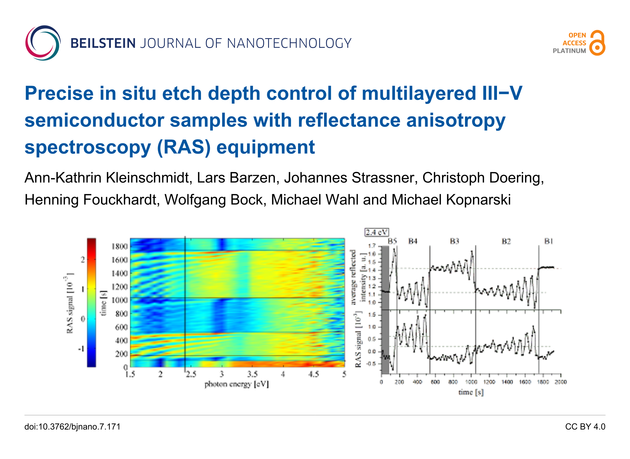
Precise in situ etch depth control of multilayered III−V semiconductor samples with reflectance anisotropy spectroscopy (RAS) equipment
Ann-Kathrin Kleinschmidt, Lars Barzen, Johannes Strassner, Christoph Doering, Henning Fouckhardt, Wolfgang Bock, Michael Wahl and Michael Kopnarski
Beilstein J. Nanotechnol. 2016, 7, 1783–1793.
https://doi.org/10.3762/bjnano.7.171
How to Cite
Kleinschmidt, A.-K.; Barzen, L.; Strassner, J.; Doering, C.; Fouckhardt, H.; Bock, W.; Wahl, M.; Kopnarski, M. Beilstein J. Nanotechnol. 2016, 7, 1783–1793. doi:10.3762/bjnano.7.171
Download Citation
Citation data can be downloaded as file using the "Download" button or used for copy/paste from the text window
below.
Citation data in RIS format can be imported by all major citation management software, including EndNote,
ProCite, RefWorks, and Zotero.
Presentation Graphic
| Picture with graphical abstract, title and authors for social media postings and presentations. | ||
| Format: PNG | Size: 1.1 MB | Download |
Citations to This Article
Up to 20 of the most recent references are displayed here.
Scholarly Works
- Lastras-Martínez, A.; Guevara-Macías, L. E.; Martínez-Espinosa, R.; Ortega-Gallegos, J.; Lastras-Montaño, M. A.; Zavala-Morán, U.; Balderas-Navarro, R. E.; Lastras-Martínez, L. F. Singular value decomposition for deconvolution and physical insight into reflectance anisotropy in zincblende semiconductors. Journal of Applied Physics 2025, 137. doi:10.1063/5.0249884
- Zhang, L.; Ouyang, C.; Wang, P.; Liu, H.; Wen, J.; Wang, C.; Ma, B.; Zhang, C.; Xing, F.; Zhao, J.; You, R.; Fan, K.; Zhao, X.; You, Z. Non-invasive in-situ monitoring of deep etching processes using terahertz metasurfaces. Optics Express 2024, 32, 46999. doi:10.1364/oe.541662
- Rodríguez-Salas, L.; Lastras-Martínez, A.; Núñez-Olvera, O. F.; Lastras-Montaño, M. A.; Castro-García, R.; Balderas-Navarro, R. E.; Lastras-Martínez, L. F. Data reduction for spatially resolved reflectance anisotropy spectrometer. The Review of scientific instruments 2023, 94. doi:10.1063/5.0162116
- Zhang, L.; Ma, H.; Sun, Z.; Wang, Z.; Fan, K.; Jin, B.; You, R.; Zhao, X.; You, Z. Terahertz Barcodes Enabled by All‐Silicon Metasurfaces for Process Control and Monitoring Applications. Advanced Materials Technologies 2023, 8. doi:10.1002/admt.202201631
- Oliveira, E.; Strassner, J.; Doering, C.; Fouckhardt, H. Reflectance anisotropy spectroscopy (RAS) for in-situ identification of roughness morphologies evolving during reactive ion etching (RIE). Applied Surface Science 2023, 611, 155769. doi:10.1016/j.apsusc.2022.155769
- Oliveira, E.; Strassner, J.; Doering, C.; Fouckhardt, H. Reactive Ion Etching (RIE) Induced Surface Roughness Precisely Monitored In-Situ and in Real Time by Reflectance Anisotropy Spectroscopy (RAS) in Combination with Principle Component Analysis (PCA). Advances in Materials Science and Engineering 2022, 2022, 1–7. doi:10.1155/2022/9747505
- Sombrio, G.; Oliveira, E.; Strassner, J.; Doering, C.; Fouckhardt, H. Interferometric in-situ III/V semiconductor dry-etch depth-control with ±0.8 nm best accuracy using a quadruple-Vernier-scale measurement. Journal of Vacuum Science & Technology B, Nanotechnology and Microelectronics: Materials, Processing, Measurement, and Phenomena 2021, 39, 052204. doi:10.1116/6.0001209
- Sombrio, G.; Oliveira, E.; Strassner, J.; Richter, J. M.; Doering, C.; Fouckhardt, H. Doped or Quantum-Dot Layers as In Situ Etch-Stop Indicators for III/V Semiconductor Reactive Ion Etching (RIE) Using Reflectance Anisotropy Spectroscopy (RAS). Micromachines 2021, 12, 502. doi:10.3390/mi12050502
- Doering, C.; Strassner, J.; Fouckhardt, H. In-situ etch-depth control better than 5 nm with reflectance anisotropy spectroscopy (RAS) equipment during reactive ion etching (RIE): A technical RAS application. AIP Advances 2019, 9, 075116. doi:10.1063/1.5099526
- Fouckhardt, H.; Kleinschmidt, A.-K.; Strassner, J.; Doering, C. Fundamental Transverse Mode Selection (TMS#0) of Broad Area Semiconductor Lasers with Integrated Twice-Retracted 4f Set-Up and Film-Waveguide Lens. Advances in OptoElectronics 2017, 2017, 1–6. doi:10.1155/2017/5283850
- Doering, C.; Kleinschmidt, A.-K.; Strassner, J.; Fouckhardt, H. Monolithically integrated fourier-optical transverse-mode selector for broad area lasers. In 2017 Conference on Lasers and Electro-Optics Europe & European Quantum Electronics Conference (CLEO/Europe-EQEC), IEEE, 2017; 1. doi:10.1109/cleoe-eqec.2017.8086404