Cite the Following Article
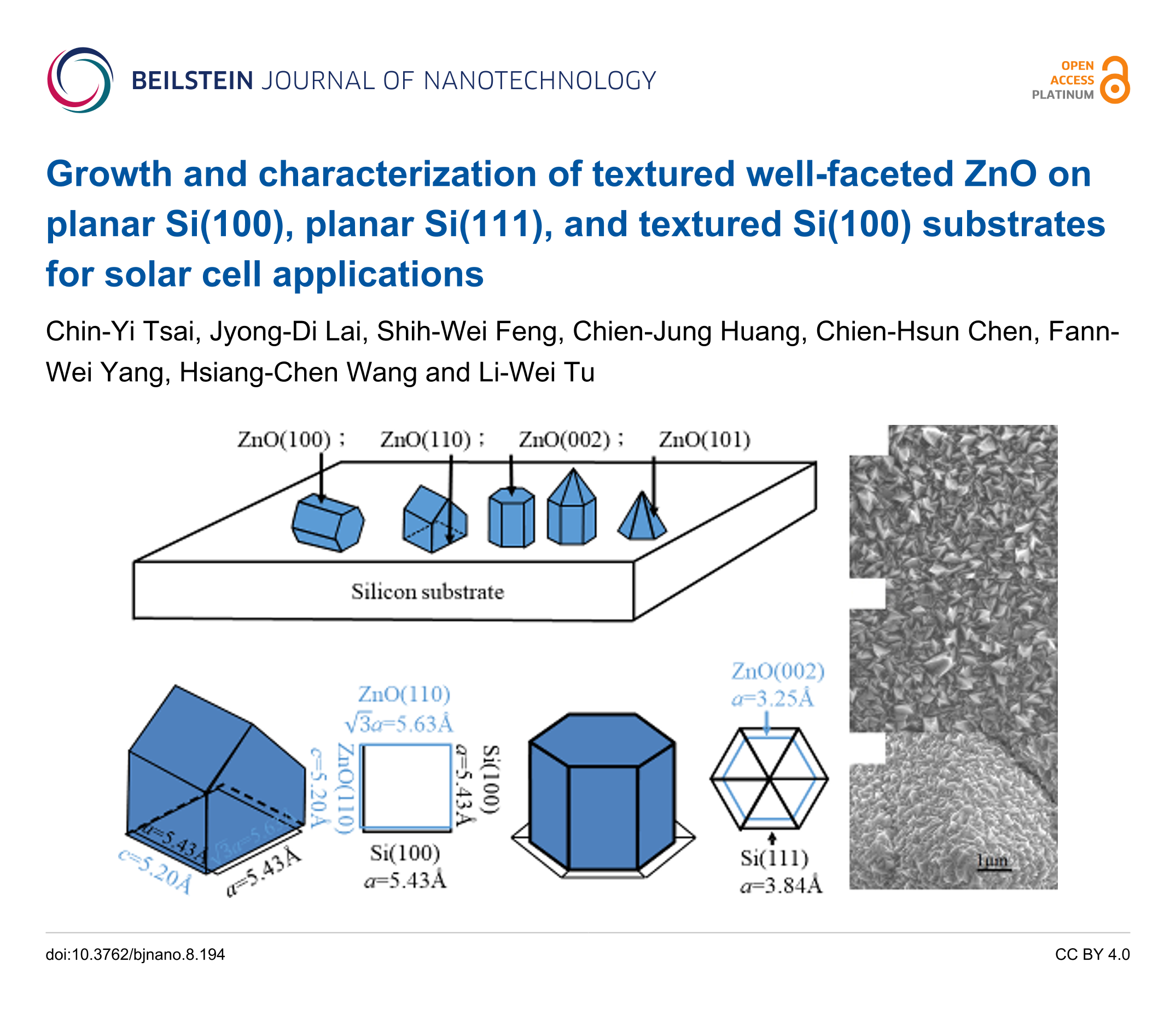
Growth and characterization of textured well-faceted ZnO on planar Si(100), planar Si(111), and textured Si(100) substrates for solar cell applications
Chin-Yi Tsai, Jyong-Di Lai, Shih-Wei Feng, Chien-Jung Huang, Chien-Hsun Chen, Fann-Wei Yang, Hsiang-Chen Wang and Li-Wei Tu
Beilstein J. Nanotechnol. 2017, 8, 1939–1945.
https://doi.org/10.3762/bjnano.8.194
How to Cite
Tsai, C.-Y.; Lai, J.-D.; Feng, S.-W.; Huang, C.-J.; Chen, C.-H.; Yang, F.-W.; Wang, H.-C.; Tu, L.-W. Beilstein J. Nanotechnol. 2017, 8, 1939–1945. doi:10.3762/bjnano.8.194
Download Citation
Citation data can be downloaded as file using the "Download" button or used for copy/paste from the text window
below.
Citation data in RIS format can be imported by all major citation management software, including EndNote,
ProCite, RefWorks, and Zotero.
Presentation Graphic
| Picture with graphical abstract, title and authors for social media postings and presentations. | ||
| Format: PNG | Size: 1011.0 KB | Download |
Citations to This Article
Up to 20 of the most recent references are displayed here.
Scholarly Works
- C, R.; Arulraj, A. Enhanced photoconductive response of ZnO thin films with the impact of annealing temperatures on structural and optical properties. Scientific reports 2025, 15, 28851. doi:10.1038/s41598-025-02177-7
- Okcu, H.; Ardila, G.; Rapenne, L.; Roussel, H.; Jiménez, C.; Muñoz-Rojas, D. Open-air deposition of submicron self-textured ZnO thin films with high piezoelectric coefficients and oxygen polarity. Applied Surface Science 2025, 696, 162945. doi:10.1016/j.apsusc.2025.162945
- Podia, M.; Tripathi, A. K. Role of shallow donor defects in inducing broad visible photoluminescence in ZnO thin film. Journal of Luminescence 2025, 280, 121083. doi:10.1016/j.jlumin.2025.121083
- Sanchez-Fernandez, L. S.; Rendon-Gomez, V. E.; Martínez-Landeros, V. H.; Falcón-Franco, L. A.; León-Puertos, C.; Hernandez-Como, N. Influence of the deposition cycles of ZnO thin films by SILAR deposition on the carbon monoxide gas sensor analysis. MRS Advances 2025, 10, 619–624. doi:10.1557/s43580-025-01137-7
- Naderi, N.; Ahmad, H.; Ismail, M. F. Improved optoelectrical performance of nanostructured ZnO/porous silicon photovoltaic devices. Ceramics International 2024, 50, 14849–14855. doi:10.1016/j.ceramint.2024.01.400
- Arifin, N. M.; Mhd Noor, E. E.; Mohamad, F.; Mohamad, N. The Impact of Spinning Speed on n-TiO2/ZnO Bilayer Thin Film Fabricated through Sol–Gel Spin-Coating Method. Coatings 2024, 14, 73. doi:10.3390/coatings14010073
- Kuzyk, O.; Dan'kiv, O.; Stolyarchuk, I.; Peleshchak, R.; Pavlovskyy, Y. The Modeling of Self-Consistent Electron–Deformation–Diffusion Effects in Thin Films with Lattice Parameter Mismatch. Coatings 2023, 13, 509. doi:10.3390/coatings13030509
- Arifin, N. M.; Mohamad, F.; Hussin, R.; Ismail, A. Z. M.; Ramli, S. A.; Ahmad, N.; Nor, N. H. M.; Sahdan, M. Z.; Zain, M. Z. M.; Izaki, M. Annealing Treatment on Homogenous n-TiO2/ZnO Bilayer Thin Film Deposition as Window Layer for p-Cu2O-Based Heterostructure Thin Film. Coatings 2023, 13, 206. doi:10.3390/coatings13010206
- Chen, W.-T.; Fang, P.-C.; Chen, Y.-W.; Chiu, S.-J.; Ku, C.-S.; Brahma, S.; Lo, K.-Y. Zn dots coherently grown as the seed and buffer layers on Si(111) for ZnO thin film: Mechanism, in situ analysis, and simulation. Journal of Vacuum Science & Technology A 2022, 40. doi:10.1116/5.0106583
- Abdallah, B.; Hussin, R.; Zetoune, W.
- Abdallah, B.; Hussin, R.; Zetoune, W. Effect of Etched Silicon Substrate on Structural, Morphological, and Optical Properties of Deposited ZnO Films via DC Sputtering. Aerosol Science and Engineering 2021, 6, 30–44. doi:10.1007/s41810-021-00122-5
- Jabbar, R. H.; Jabbar, S. J.; Shakir, W. A.; Abdulsattar, M. A.; Hilal, I. H. Synthesis of ZnO: Sb thin films Dropped on glass and Porous Silicon for CO Gas Sensing. Journal of Physics: Conference Series 2021, 1963, 012008. doi:10.1088/1742-6596/1963/1/012008
- Prepelita, P.; Garoi, F.; Craciun, V. Structural and optical characteristics determined by the sputtering deposition conditions of oxide thin films. Beilstein journal of nanotechnology 2021, 12, 354–365. doi:10.3762/bjnano.12.29
- Rani, M.; Kashyap, J.; Singh, U.; Kapoor, A. Impact of fabrication of pyramidal structure on silicon wafer surface in ZnO/Si heterojunction. In AIP Conference Proceedings, AIP Publishing, 2020; pp 020179 ff. doi:10.1063/5.0001996
- Chen, C.-H.; Lai, J.-D.; Tsai, C.-Y.; Feng, S.-W.; Cheng, T.-H.; Wang, H.-C.; Tu, L.-W. Growth, characterization, and analysis of the nanostructures of ZnO:B thin films grown on ITO glass substrates by a LPCVD: a study on the effects of boron doping. Journal of Materials Science: Materials in Electronics 2019, 30, 5698–5705. doi:10.1007/s10854-019-00863-7