Abstract
Spatially resolved measurements of the apparent tunneling barrier height Φapp in scanning tunneling microscopy have been used to estimate variations of the local work function Φ of surface structures. We experimentally show that Φapp can fail as a measure of Φ. The discrepancies are attributed to a kinetic-energy contribution to Φapp. This contribution depends on the lateral extent of the tunneling current filament and, consequently, on the local surface structure.
Findings
The work function of a metal surface [1], the work required at temperature T = 0 K to move an electron from the metal to infinity, is relevant for, e.g.,the behavior of electronic devices [2], the energetics of molecules at surfaces [3], including reactions [4,5], and electronic states confined near surfaces [6]. Practical surfaces are finite in size and contain plenty of inhomogeneities that cause local variations of the electrostatic potential. This is reflected by the notion of a local work function Φ [7-9]. Adsorbates modify Φ in an intriguing manner [10-13]. In turn, variations of Φ produce, e.g., atomic-scale contrast in field-emission microscopy, photo-emission electron microscopy, and low-energy electron microscopy [14-16].
Atomic steps are a well-known example of a structure that affects the local work function Φ. The spill-out of electrons from a planar crystal surface creates a dipole layer that increases Φ [17,18]. Steps modify the spill-out and thus reduce Φ [19] as observed by Kelvin probe measurements [20] and photoelectron spectroscopy [9].
The concept of a local work function is particularly relevant for scanning tunneling microscopy [7,8]. In the most simple one-dimensional model the exponential variation of the tunneling current I at low bias with the tip–sample distance z is directly related to the average of the work function ![[Graphic 1]](/bjnano/content/inline/2190-4286-9-283-i1.svg?max-width=637&scale=1.18182) of the tip and the sample [21,22]. A closer look shows that factors like the image potential of the tunneling electron or the electronic structure of the electrodes complicate matters [23-26]. I still varies exponentially with z, but
of the tip and the sample [21,22]. A closer look shows that factors like the image potential of the tunneling electron or the electronic structure of the electrodes complicate matters [23-26]. I still varies exponentially with z, but ![[Graphic 2]](/bjnano/content/inline/2190-4286-9-283-i2.svg?max-width=637&scale=1.18182) is replaced with an apparent barrier height Φapp [27]. Although there is no simple expression connecting Φapp and the local work function of the sample Φ (partially because the tip structure is usually unknown), it is common practice to assume that measured variations of Φapp represent those of Φ [28-31].
is replaced with an apparent barrier height Φapp [27]. Although there is no simple expression connecting Φapp and the local work function of the sample Φ (partially because the tip structure is usually unknown), it is common practice to assume that measured variations of Φapp represent those of Φ [28-31].
Here we experimentally show that Φapp can fail as a measure of Φ. I(z) data from Cu atoms arranged in extended single-atom rows and double rows as well as from trenches of single-atom depth are analyzed. Φapp determined from these data varies significantly, but the variation is opposite to the expected trend of the local sample work function. We explain this observation in terms of the lateral extent of the tunneling-current filament. While an atomic asperity at the sample is expected to exhibit a reduced Φ, it simultaneously reduces the lateral range over which a significant part of the current flows. This effectively raises the energy required to overcome the potential barrier between the tip and the sample.
In the context of the scanning tunneling microscope, the idea of an increased barrier due to lateral confinement has been attributed to J. Tersoff in [27]. Lateral confinement plays a key role in ballistic transport through nanoscale constrictions [32] and was suggested to affect the apparent barrier height in single-atom contacts [33]. Atomistic transport calculations have been performed for Au contacts in [34]. Symmetric junctions comprised of two (001) surfaces, either planar or with an adatom or with a five-atom pyramid, were considered. The apparent barrier heights extracted were 5.7, 6.7, and 6.8 eV, respectively. Because of a systematic error of the local density approximation used in the calculations [34], the value of the flat surface is larger than the experimental one [35]. However, the trend of a barrier height increase with decreased lateral size of the tunneling-current path is expected to be reliable. These results predict a kinetic energy contribution of the order of 1 eV for tunneling between two atomically sharp structures.
Experiments were performed in an ultrahigh vacuum STM operated at 4.5 K. Cu(111) surfaces were cleaned by Ar+ sputter/anneal cycles. W tips were electrochemically etched from polycrystalline wire. After sputtering, they were further prepared in situ by indenting them into the Cu(111) substrate. Because of this procedure, the tips were presumably covered with Cu.
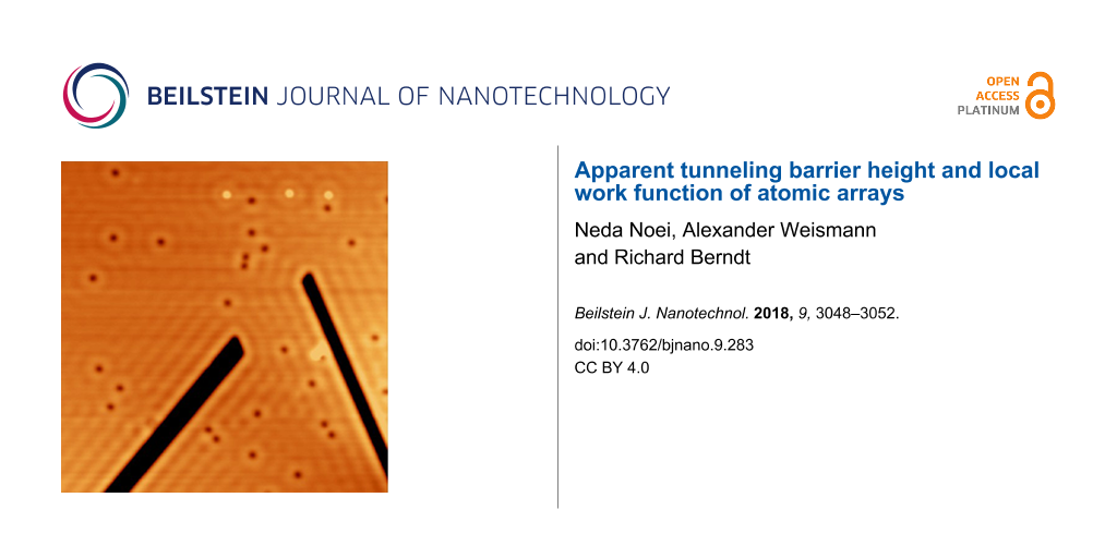
In surface areas close to the point of indentation (typical distance 200 nm) long, straight atomic chains are formed on the substrate (Figure 1). While the width of the chains varies, one- and two-atom wide chains are frequently observed. They may be identified from their apparent widths in topographs and from a characteristic signature in differential conductance (dI/dV) spectra. As first reported by Fölsch et al., short single-atom Cu chains on Cu(111) exhibit an unoccupied resonance at 1.5 eV above the Fermi energy EF [36]. Closely related data including the limit of very long chains were reported from chains on Ag(111) [37]. In addition to chains, we occasionally observed long trenches of varying widths with an apparent depth of one atomic layer or less (Figure 1). Finally, single Cu adatoms were prepared by transfer from the tip to the surface [33].
![[2190-4286-9-283-1]](/bjnano/content/figures/2190-4286-9-283-1.png?scale=2.0&max-width=1024&background=FFFFFF)
Figure 1: STM images of a Cu(111) surface with chains and trenches of monolayer height. (a) A Cu chain approximately two atoms wide and a parallel trench. (b) Two wide trenches (approx. 2 and 3 atoms) with deposited single Cu atoms. (c) Monatomic chains and trenches. The images were acquired at (a) V = 20 mV and I = 3 nA and (b, c) V = 100 mV and I = 5 nA.
Figure 1: STM images of a Cu(111) surface with chains and trenches of monolayer height. (a) A Cu chain approx...
To measure the current I as a function of the vertical tip excursion Δz the feedback loop of the STM was disabled at a sample voltage of V = 20 mV and a current of I = 200 pA. The tip was then brought closer to the structure under investigation at a rate of 1.7 nm/s while recording I. Figure 2 shows typical results from a clean (111) terrace, a Cu adatom, a monatomic chain, a wide chain, and grooves of monolayer depth with single-atom or wider width. There are systematic differences between the slopes of the terrace data (black line) and the other data sets (colors). On asperities such as adatoms and narrow chains the current varies more rapidly, on narrow trenches the slope is reduced. The slopes observed on wide trenches and chains are close to the terrace data.
![[2190-4286-9-283-2]](/bjnano/content/figures/2190-4286-9-283-2.png?scale=2.0&max-width=1024&background=FFFFFF)
Figure 2: Current–distance data I(Δz). Negative values of Δz indicate reduced tip–sample distances with respect to the initial separation defined by I = 200 pA and V = 20 mV. Data recorded from a (111) terrace (black), a Cu adatom, a monatomic chain, a wider chain (approx. 2 atoms), and trenches of monolayer depth with single-atom and wider width (approx. 2 atoms) are displayed. The curves are arbitrarily offset along the ordinate for clarity. The terrace data are shown with each curve for comparison. Small undulations of the data are due to low-frequency vibration of the microscope.
Figure 2: Current–distance data I(Δz). Negative values of Δz indicate reduced tip–sample distances with respe...
The apparent barrier heights Φeff, which we extracted from the exponential variation of the current ![[Graphic 3]](/bjnano/content/inline/2190-4286-9-283-i3.svg?max-width=637&scale=1.18182) , are presented in Table 1. These values were measured with the same tip apex. The absolute values are obtained using the calibration of the piezoelectric transducer, which leads to an estimated uncertainty of 10%. The ratios between them, however, are not affected. The maximal apparent barrier height is measured on Cu adatoms. It exceeds the minimal value, which is observed from monatomic trenches, by approx. 0.9 eV and is 0.3 eV larger than on flat terraces. Repetition of the measurements at another low bias voltage (V = 10 mV) led to virtually identical results as expected.
, are presented in Table 1. These values were measured with the same tip apex. The absolute values are obtained using the calibration of the piezoelectric transducer, which leads to an estimated uncertainty of 10%. The ratios between them, however, are not affected. The maximal apparent barrier height is measured on Cu adatoms. It exceeds the minimal value, which is observed from monatomic trenches, by approx. 0.9 eV and is 0.3 eV larger than on flat terraces. Repetition of the measurements at another low bias voltage (V = 10 mV) led to virtually identical results as expected.
Table 1: Apparent barrier heights Φapp extracted from Figure 2.
| structure | Φapp (eV) |
|---|---|
| (111) terrace | 3.9 |
| adatom | 4.2 |
| monatomic chain | 4.2 |
| wide chain | 4.0 |
| monatomic trench | 3.3 |
| wide trench | 3.8 |
The electron spill-out at steps is associated with a dipole moment [19]. It counteracts the dipole present at flat surfaces and therefore reduces the work function. Atomic chains and single atoms represent stronger corrugations of a surface and therefore are expected to further enhance this effect. The observed trend of Φapp, however, is opposite to this expectation.
Φapp may vary when the local surface normal is at an angle α with the z direction of the STM [38]. However, this is expected to reduce Φapp by a factor cos2α and thus cannot explain our large experimental values. In any event, we measured Φapp of atoms and chains on maxima of the topographies, where α ≈ 0.
We therefore attribute the peculiar variation of Φapp at adatoms and chains to the kinetic-energy contribution that was proposed in earlier theoretical works [27,33,34]. Considering the topographies of adatoms and chains, the lateral extension of the tunneling current filament is expected to be narrower on these structures than on flat terraces. The trend of the experimental Φapp data is consistent with these expectations and the theoretical results of [34]. A quantitative estimate of the kinetic-energy contributions has to take into account the local work function of the structures under investigation. Unfortunately, neither experimental nor theoretical data are currently available for the structures of Figure 1.
The data from trenches require an additional consideration. When the tip is centered above a trench, a part of the tunneling current is expected to flow to the edge atoms of the adjacent terraces. Indeed, the apparent depth of single-atom trenches is significantly smaller than a step height. On one hand, this contribution to the current widens the current filament. On the other hand, it is not perpendicular to the surface normal and consequently the geometric factor introduced above may play a role and reduce Φapp.
In conclusion, topographic features determine the extent of the electron wave function across the tunneling path in the STM and thus add a kinetic energy contribution to the apparent barrier height Φapp. The difference of this contribution between atomic protrusions and trenches is of the order of 1 eV. This complicates the relation between the local sample work function Φ and the measured Φapp. The shape of the tip also influences the degree of confinement and presumably contributes to the scatter of Φapp observed with different tips.
References
-
Derry, G. N.; Kern, M. E.; Worth, E. H. J. Vac. Sci. Technol., A 2015, 33, 060801. doi:10.1116/1.4934685
Return to citation in text: [1] -
Kahn, A. Mater. Horiz. 2016, 3, 7–10. doi:10.1039/c5mh00160a
Return to citation in text: [1] -
Jiang, Y.; Li, J.; Su, G.; Ferri, N.; Liu, W.; Tkatchenko, A. J. Phys.: Condens. Matter 2017, 29, 204001. doi:10.1088/1361-648x/aa693e
Return to citation in text: [1] -
Lang, N. D.; Holloway, S.; Nørskov, J. K. Surf. Sci. 1985, 150, 24–38. doi:10.1016/0039-6028(85)90208-0
Return to citation in text: [1] -
Vayenas, C. G.; Bebelis, S.; Ladas, S. Nature 1990, 343, 625–627. doi:10.1038/343625a0
Return to citation in text: [1] -
Fischer, R.; Schuppler, S.; Fischer, N.; Fauster, T.; Steinmann, W. Phys. Rev. Lett. 1993, 70, 654–657. doi:10.1103/physrevlett.70.654
Return to citation in text: [1] -
Binnig, G.; Rohrer, H.; Gerber, C.; Weibel, E. Phys. Rev. Lett. 1982, 49, 57–61. doi:10.1103/physrevlett.49.57
Return to citation in text: [1] [2] -
Binnig, G.; Rohrer, H. Surf. Sci. 1983, 126, 236–244. doi:10.1016/0039-6028(83)90716-1
Return to citation in text: [1] [2] -
Wandelt, K. Appl. Surf. Sci. 1997, 111, 1. doi:10.1016/s0169-4332(96)00692-7
Return to citation in text: [1] [2] -
Michaelides, A.; Hu, P.; Lee, M.-H.; Alavi, A.; King, D. A. Phys. Rev. Lett. 2003, 90, 246103. doi:10.1103/physrevlett.90.246103
Return to citation in text: [1] -
Ploigt, H.-C.; Brun, C.; Pivetta, M.; Patthey, F.; Schneider, W.-D. Phys. Rev. B 2007, 76, 195404. doi:10.1103/physrevb.76.195404
Return to citation in text: [1] -
Bagus, P. S.; Käfer, D.; Witte, G.; Wöll, C. Phys. Rev. Lett. 2008, 100, 126101. doi:10.1103/physrevlett.100.126101
Return to citation in text: [1] -
Roman, T.; Groß, A. Phys. Rev. Lett. 2013, 110, 156804. doi:10.1103/physrevlett.110.156804
Return to citation in text: [1] -
Müller, E. W. Z. Phys. 1937, 106, 541–550. doi:10.1007/bf01339895
Return to citation in text: [1] -
Bauer, E. Surf. Rev. Lett. 1998, 5, 1275–1286. doi:10.1142/s0218625x98001614
Return to citation in text: [1] -
Rotermund, H. H. Surf. Sci. Rep. 1997, 29, 265–364. doi:10.1016/s0167-5729(97)00012-5
Return to citation in text: [1] -
Seitz, F. Modern Theory of Solids; McGraw-Hill Education, 1940.
Return to citation in text: [1] -
Lang, N. D.; Kohn, W. Phys. Rev. B 1971, 3, 1215–1223. doi:10.1103/physrevb.3.1215
Return to citation in text: [1] -
Smoluchowski, R. Phys. Rev. 1941, 60, 661–674. doi:10.1103/physrev.60.661
Return to citation in text: [1] [2] -
Besocke, K.; Krahl-Urban, B.; Wagner, H. Surf. Sci. 1977, 68, 39–46. doi:10.1016/0039-6028(77)90187-x
Return to citation in text: [1] -
Simmons, J. G. J. Appl. Phys. 1963, 34, 1793–1803. doi:10.1063/1.1702682
Return to citation in text: [1] -
Simmons, J. G. J. Appl. Phys. 1963, 34, 2581–2590. doi:10.1063/1.1729774
Return to citation in text: [1] -
Binnig, G.; Garcia, N.; Rohrer, H.; Soler, J. M.; Flores, F. Phys. Rev. B 1984, 30, 4816–4818. doi:10.1103/physrevb.30.4816
Return to citation in text: [1] -
Becker, M.; Berndt, R. Phys. Rev. B 2010, 81, 035426. doi:10.1103/physrevb.81.035426
Return to citation in text: [1] -
Becker, M.; Berndt, R. Appl. Phys. Lett. 2010, 96, 033112. doi:10.1063/1.3291114
Return to citation in text: [1] -
Pitarke, J. M.; Echenique, P. M.; Flores, F. Surf. Sci. 1989, 217, 267–275. doi:10.1016/0039-6028(89)90548-7
Return to citation in text: [1] -
Lang, N. D. Phys. Rev. B 1988, 37, 10395–10398. doi:10.1103/physrevb.37.10395
Return to citation in text: [1] [2] [3] -
Jia, J. F.; Inoue, K.; Hasegawa, Y.; Yang, W. S.; Sakurai, T. Phys. Rev. B 1998, 58, 1193–1196. doi:10.1103/physrevb.58.1193
Return to citation in text: [1] -
Sasaki, M.; Yamamoto, S. Shinku (1958-2007) 2007, 50, 313–318. doi:10.3131/jvsj.50.313
Return to citation in text: [1] -
Herz, M.; Schiller, C.; Giessibl, F. J.; Mannhart, J. Appl. Phys. Lett. 2005, 86, 153101. doi:10.1063/1.1900316
Return to citation in text: [1] -
Altenburg, S. J.; Berndt, R. New J. Phys. 2014, 16, 053036. doi:10.1088/1367-2630/16/5/053036
Return to citation in text: [1] -
Ihn, T. Semiconductor Nanostructures; Oxford University Press: Oxford, United Kingdom, 2009. doi:10.1093/acprof:oso/9780199534425.001.0001
Return to citation in text: [1] -
Limot, L.; Kröger, J.; Berndt, R.; Garcia-Lekue, A.; Hofer, W. A. Phys. Rev. Lett. 2005, 94, 126102. doi:10.1103/physrevlett.94.126102
Return to citation in text: [1] [2] [3] -
Garcia-Lekue, A.; Wang, L. W. Phys. Rev. B 2010, 82, 035410. doi:10.1103/physrevb.82.035410
Return to citation in text: [1] [2] [3] [4] -
Fauster, T.; Steinmann, W. Two-photon photoemission spectroscopy of image states. In Photonic Probes of Surfaces; Helvi, P., Ed.; Electromagnetic Waves: Recent Developments in Research, Vol. 2; Elsevier: Amsterdam, Netherlands, 1995; pp 347–411. doi:10.1016/b978-0-444-82198-0.50015-1
Return to citation in text: [1] -
Fölsch, S.; Hyldgaard, P.; Koch, R.; Ploog, K. H. Phys. Rev. Lett. 2004, 92, 056803. doi:10.1103/physrevlett.92.056803
Return to citation in text: [1] -
Sperl, A.; Kröger, J.; Néel, N.; Jensen, H.; Berndt, R.; Franke, A.; Pehlke, E. Phys. Rev. B 2008, 77, 085422. doi:10.1103/physrevb.77.085422
Return to citation in text: [1] -
Binnig, G.; Rohrer, H. IBM J. Res. Dev. 1986, 30, 355.
Return to citation in text: [1]
| 27. | Lang, N. D. Phys. Rev. B 1988, 37, 10395–10398. doi:10.1103/physrevb.37.10395 |
| 33. | Limot, L.; Kröger, J.; Berndt, R.; Garcia-Lekue, A.; Hofer, W. A. Phys. Rev. Lett. 2005, 94, 126102. doi:10.1103/physrevlett.94.126102 |
| 34. | Garcia-Lekue, A.; Wang, L. W. Phys. Rev. B 2010, 82, 035410. doi:10.1103/physrevb.82.035410 |
| 34. | Garcia-Lekue, A.; Wang, L. W. Phys. Rev. B 2010, 82, 035410. doi:10.1103/physrevb.82.035410 |
| 1. | Derry, G. N.; Kern, M. E.; Worth, E. H. J. Vac. Sci. Technol., A 2015, 33, 060801. doi:10.1116/1.4934685 |
| 6. | Fischer, R.; Schuppler, S.; Fischer, N.; Fauster, T.; Steinmann, W. Phys. Rev. Lett. 1993, 70, 654–657. doi:10.1103/physrevlett.70.654 |
| 23. | Binnig, G.; Garcia, N.; Rohrer, H.; Soler, J. M.; Flores, F. Phys. Rev. B 1984, 30, 4816–4818. doi:10.1103/physrevb.30.4816 |
| 24. | Becker, M.; Berndt, R. Phys. Rev. B 2010, 81, 035426. doi:10.1103/physrevb.81.035426 |
| 25. | Becker, M.; Berndt, R. Appl. Phys. Lett. 2010, 96, 033112. doi:10.1063/1.3291114 |
| 26. | Pitarke, J. M.; Echenique, P. M.; Flores, F. Surf. Sci. 1989, 217, 267–275. doi:10.1016/0039-6028(89)90548-7 |
| 4. | Lang, N. D.; Holloway, S.; Nørskov, J. K. Surf. Sci. 1985, 150, 24–38. doi:10.1016/0039-6028(85)90208-0 |
| 5. | Vayenas, C. G.; Bebelis, S.; Ladas, S. Nature 1990, 343, 625–627. doi:10.1038/343625a0 |
| 27. | Lang, N. D. Phys. Rev. B 1988, 37, 10395–10398. doi:10.1103/physrevb.37.10395 |
| 3. | Jiang, Y.; Li, J.; Su, G.; Ferri, N.; Liu, W.; Tkatchenko, A. J. Phys.: Condens. Matter 2017, 29, 204001. doi:10.1088/1361-648x/aa693e |
| 7. | Binnig, G.; Rohrer, H.; Gerber, C.; Weibel, E. Phys. Rev. Lett. 1982, 49, 57–61. doi:10.1103/physrevlett.49.57 |
| 8. | Binnig, G.; Rohrer, H. Surf. Sci. 1983, 126, 236–244. doi:10.1016/0039-6028(83)90716-1 |
| 21. | Simmons, J. G. J. Appl. Phys. 1963, 34, 1793–1803. doi:10.1063/1.1702682 |
| 22. | Simmons, J. G. J. Appl. Phys. 1963, 34, 2581–2590. doi:10.1063/1.1729774 |
| 17. | Seitz, F. Modern Theory of Solids; McGraw-Hill Education, 1940. |
| 18. | Lang, N. D.; Kohn, W. Phys. Rev. B 1971, 3, 1215–1223. doi:10.1103/physrevb.3.1215 |
| 20. | Besocke, K.; Krahl-Urban, B.; Wagner, H. Surf. Sci. 1977, 68, 39–46. doi:10.1016/0039-6028(77)90187-x |
| 14. | Müller, E. W. Z. Phys. 1937, 106, 541–550. doi:10.1007/bf01339895 |
| 15. | Bauer, E. Surf. Rev. Lett. 1998, 5, 1275–1286. doi:10.1142/s0218625x98001614 |
| 16. | Rotermund, H. H. Surf. Sci. Rep. 1997, 29, 265–364. doi:10.1016/s0167-5729(97)00012-5 |
| 10. | Michaelides, A.; Hu, P.; Lee, M.-H.; Alavi, A.; King, D. A. Phys. Rev. Lett. 2003, 90, 246103. doi:10.1103/physrevlett.90.246103 |
| 11. | Ploigt, H.-C.; Brun, C.; Pivetta, M.; Patthey, F.; Schneider, W.-D. Phys. Rev. B 2007, 76, 195404. doi:10.1103/physrevb.76.195404 |
| 12. | Bagus, P. S.; Käfer, D.; Witte, G.; Wöll, C. Phys. Rev. Lett. 2008, 100, 126101. doi:10.1103/physrevlett.100.126101 |
| 13. | Roman, T.; Groß, A. Phys. Rev. Lett. 2013, 110, 156804. doi:10.1103/physrevlett.110.156804 |
| 7. | Binnig, G.; Rohrer, H.; Gerber, C.; Weibel, E. Phys. Rev. Lett. 1982, 49, 57–61. doi:10.1103/physrevlett.49.57 |
| 8. | Binnig, G.; Rohrer, H. Surf. Sci. 1983, 126, 236–244. doi:10.1016/0039-6028(83)90716-1 |
| 9. | Wandelt, K. Appl. Surf. Sci. 1997, 111, 1. doi:10.1016/s0169-4332(96)00692-7 |
| 32. | Ihn, T. Semiconductor Nanostructures; Oxford University Press: Oxford, United Kingdom, 2009. doi:10.1093/acprof:oso/9780199534425.001.0001 |
| 28. | Jia, J. F.; Inoue, K.; Hasegawa, Y.; Yang, W. S.; Sakurai, T. Phys. Rev. B 1998, 58, 1193–1196. doi:10.1103/physrevb.58.1193 |
| 29. | Sasaki, M.; Yamamoto, S. Shinku (1958-2007) 2007, 50, 313–318. doi:10.3131/jvsj.50.313 |
| 30. | Herz, M.; Schiller, C.; Giessibl, F. J.; Mannhart, J. Appl. Phys. Lett. 2005, 86, 153101. doi:10.1063/1.1900316 |
| 31. | Altenburg, S. J.; Berndt, R. New J. Phys. 2014, 16, 053036. doi:10.1088/1367-2630/16/5/053036 |
| 27. | Lang, N. D. Phys. Rev. B 1988, 37, 10395–10398. doi:10.1103/physrevb.37.10395 |
| 33. | Limot, L.; Kröger, J.; Berndt, R.; Garcia-Lekue, A.; Hofer, W. A. Phys. Rev. Lett. 2005, 94, 126102. doi:10.1103/physrevlett.94.126102 |
| 36. | Fölsch, S.; Hyldgaard, P.; Koch, R.; Ploog, K. H. Phys. Rev. Lett. 2004, 92, 056803. doi:10.1103/physrevlett.92.056803 |
| 37. | Sperl, A.; Kröger, J.; Néel, N.; Jensen, H.; Berndt, R.; Franke, A.; Pehlke, E. Phys. Rev. B 2008, 77, 085422. doi:10.1103/physrevb.77.085422 |
| 34. | Garcia-Lekue, A.; Wang, L. W. Phys. Rev. B 2010, 82, 035410. doi:10.1103/physrevb.82.035410 |
| 35. | Fauster, T.; Steinmann, W. Two-photon photoemission spectroscopy of image states. In Photonic Probes of Surfaces; Helvi, P., Ed.; Electromagnetic Waves: Recent Developments in Research, Vol. 2; Elsevier: Amsterdam, Netherlands, 1995; pp 347–411. doi:10.1016/b978-0-444-82198-0.50015-1 |
| 33. | Limot, L.; Kröger, J.; Berndt, R.; Garcia-Lekue, A.; Hofer, W. A. Phys. Rev. Lett. 2005, 94, 126102. doi:10.1103/physrevlett.94.126102 |
| 34. | Garcia-Lekue, A.; Wang, L. W. Phys. Rev. B 2010, 82, 035410. doi:10.1103/physrevb.82.035410 |
© 2018 Noei et al.; licensee Beilstein-Institut.
This is an Open Access article under the terms of the Creative Commons Attribution License (http://creativecommons.org/licenses/by/4.0). Please note that the reuse, redistribution and reproduction in particular requires that the authors and source are credited.
The license is subject to the Beilstein Journal of Nanotechnology terms and conditions: (https://www.beilstein-journals.org/bjnano)