This search combines search strings from the content search (i.e. "Full Text", "Author", "Title", "Abstract", or "Keywords") with "Article Type" and "Publication Date Range" using the AND operator.
Beilstein J. Nanotechnol. 2026, 17, 1016–1027, doi:10.3762/bjnano.17.69
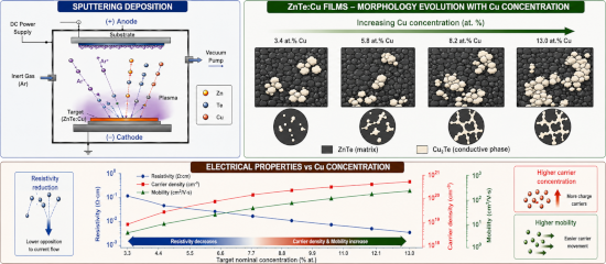
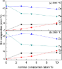
Figure 1: Chemical composition of CuZnTeO films as a function of the nominal Cu and O concentration in target...
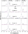
Figure 2: X-ray diffraction patterns of ZnTe and CuZnTeO films as a function of nominal Cu and O concentratio...
Figure 3: Deconvolution of the main peak the (111) plane of the cubic phase and the (200) plane of the hexago...
Figure 4: Surface micrograph and Raman spectra of CuZnTeO film with a nominal concentration of 3 atom % of Cu...
Figure 5: SEM images and X-ray diffraction of CuZnTeO films with nominal concentration of Cu and O of 3 atom ...
Figure 6: Transmittance spectra and SEM micrographs of CuZnTeO films grown on glass substrates as a function ...
Figure 7: Electrical charge transport properties of CuZnTeO films grown on glass substrates as a function of ...
Beilstein J. Nanotechnol. 2020, 11, 703–716, doi:10.3762/bjnano.11.58
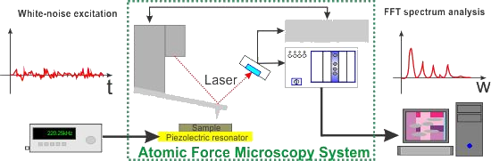
Figure 1: Experimental setup for S-AFAM, using a NI PXIe-1073 device and a function waveform generator HP/Agi...
Figure 2: Contact resonance frequencies for a graphite film on a glass substrate. a) Resonance flexural modes...
Figure 3: AFM system, the piezoelectrical signal excitation is considered to be the input, while the deflecti...
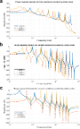
Figure 4: PSD simulation. a) Free cantilever: L = 300 μm(blue line), L = 400 μm (dashed red line) and L = 500...
Figure 5: Flexural resonance frequencies as a function of the contact stiffness for a cantilever with the fol...
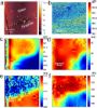
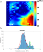
Figure 6: Results for a graphite film on a glass substrate. a) Conventional AFM topography; b) RT-AFAM for 18...
Figure 7: Results for a graphite film on a glass substrate: a) indentation modulus mapping and b) histogram f...