This search combines search strings from the content search (i.e. "Full Text", "Author", "Title", "Abstract", or "Keywords") with "Article Type" and "Publication Date Range" using the AND operator.
Beilstein J. Nanotechnol. 2025, 16, 551–560, doi:10.3762/bjnano.16.43
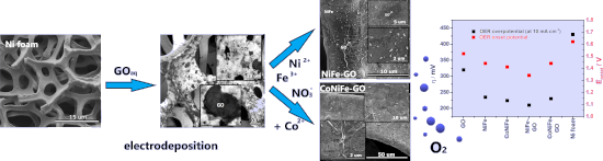
Figure 1: (a) Figure 1a was reprinted from [1], Acta Materialia, vol. 267, by A. Das; C. Latouche; S. Jobic; E. Gautron; ...
Figure 2: Raman spectra for undoped ZnO (Zn900), CZ900_Pris, CZ900_113O, CZ900_313O, CZ900_113Ag, and CZ900_3...
Figure 3: Plane view scanning electron microscopic images for CZ900_Pris (a), CZ900_313O (b), and CZ900_313Ag...
Figure 4: O K (a) and Zn L3,2 (b) XANES spectra for CZ900_Pris, CZ900_313O, and Z900_313Ag thin films.
Figure 5: X-ray photoelectron spectra for Cd 3d5/2 (a), Zn 2p3/2 (b), O 1s (c), and Si 2p3/2 (d) edges for CZ...
Figure 6: Plot showing lattice temperature as a function of time using thermal spike code to track diameter c...
Beilstein J. Nanotechnol. 2023, 14, 420–433, doi:10.3762/bjnano.14.34
Figure 1: Chronoamperometric graphs recorded during electrochemical deposition of the catalysts on nickel foa...
Figure 2: SEM images and corresponding EDX maps of NiFe (a), NiFe-GO (b), CoNiFe (c), and CoNiFe-GO (d) depos...
Figure 3: Normalized XAS spectra (a–d) and XRD patterns (e) of NiFe, CoNiFe, NiFe-GO, and CoNiFe-GO.
Figure 4: XPS high-resolution spectra of Ni 2p (a), Fe 2p (b), Co 2p (c), and C 1s (d) levels of the catalyst...
Figure 5: Linear scan voltammetry profiles (a) with corresponding evolutions of the OER overpotential η (10 m...
Figure 6: Linear scan voltammetry profiles (a) with corresponding Tafel plots (b) and evolution of the OER ov...
Figure 7: Linear scan voltammetry profiles (a) with corresponding Tafel plots (b) and evolution of the OER ov...
Figure 8: Chronopotentiometric curves recorded in aqueous solution of 1 M KOH at 10 mA∙cm−2geo (a) and SEM im...