


Search results
Search for "work function" in Full Text gives 151 result(s) in Beilstein Journal of Nanotechnology.
Defects in oxide surfaces studied by atomic force and scanning tunneling microscopy
Beilstein J. Nanotechnol. 2011, 2, 1–14, doi:10.3762/bjnano.2.1
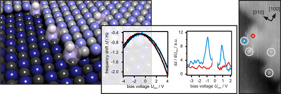
- force microscopy; scanning tunneling microscopy; thin films; work function; Review Introduction The chemical properties of many crystal surfaces, especially oxides, are significantly influenced by defects in the perfectly ordered structure [1][2][3][4][5]. These defects can be impurities in the surface
- material with the lower work function (here tip) flow to the material with the higher work function. The Fermi levels align and an electrical field is built up [21]. The contact potential ΔΦ is then given by the difference in work function of the tip and of the sample surface, which may contain the studied
- single point defects or single adsorbates, instead of integrating over a square millimeter range. However, absolute values of the work function cannot be measured directly, only work function differences. Point defects Oxygen vacancies, also known as color centers, are electron trapping point defects and


Other Beilstein-Institut Open Science Activities



