


Search results
Search for "nanowire" in Full Text gives 182 result(s) in Beilstein Journal of Nanotechnology.
Direct-write polymer nanolithography in ultra-high vacuum
Beilstein J. Nanotechnol. 2012, 3, 52–56, doi:10.3762/bjnano.3.6
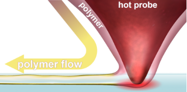
- found that monolayer-by-monolayer control of the film thickness, as previously established under nitrogen, is also possible under UHV. Figure 2 shows two polymer nanowire lines written at different speeds. Assuming a thickness of 2.6 nm for each PDDT monolayer as previously determined by XRD [14], the


X-ray spectroscopy characterization of self-assembled monolayers of nitrile-substituted oligo(phenylene ethynylene)s with variable chain length
Beilstein J. Nanotechnol. 2012, 3, 12–24, doi:10.3762/bjnano.3.2
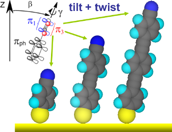
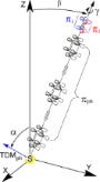
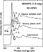
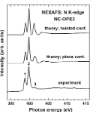
- [12][13][14][15][16][17][18], in-wire junctions [9], and cross-nanowire junctions [19]. For most of these measurements the molecular wires were assembled on a conductive substrate, serving as the bottom electrode, by using self-assembled monolayer (SAM) methods. For this purpose, oligomeric chains



Approaches to nanostructure control and functionalizations of polymer@silica hybrid nanograss generated by biomimetic silica mineralization on a self-assembled polyamine layer
Beilstein J. Nanotechnol. 2011, 2, 760–773, doi:10.3762/bjnano.2.84
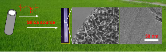
- transformation [7]. Silica nanowire films can be fabricated by catalyst-promoted vapor–liquid–solid (VLS) or solid–liquid–solid (SLS) processes under high temperature conditions, where metallic nanoparticles such as gold, gallium, and tin as catalysts are generally used to improve nanowire nucleation and growth
- crystalline self-assembly on substrates, we also synthesized an ultrathin silica-nanowire-based surface, which demonstrated the feasible modulation of the hierarchical nanostructure and surface morphology [34]. In comparison, the modulation of the nanostructure and surface morphology of nanoribbon-based
- -quality nanograss surface composed of a nanowire-based network structure, with a film thickness of about 300 nm. This is different to those films formed by using hot LPEI solution in either pure water or water–methanol (3:7 v/v), both of which tended to form LPEI@silica with a ribbon nanostructure and


Lifetime analysis of individual-atom contacts and crossover to geometric-shell structures in unstrained silver nanowires
Beilstein J. Nanotechnol. 2011, 2, 740–745, doi:10.3762/bjnano.2.81
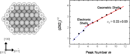
- contacting atoms by analogy with the “magic” configurations in metal cluster. In geometric shells the free energy is lowered by the change of surface energy when completing a layer of atoms on the nanowire facets, which is also known from cluster physics [20][21]. Both the electronic- and the geometric-shell
- effects and finally accomplishing the crossover to the filling of complete geometric shells corresponding to crystallographic facets of the nanowire. A detailed lifetime analysis for selected contacts helps us to obtain a detailed understanding of the correlation between the physics of quantized
- quantization. Due to the proportionality of (G/G0)1/2 to the contact radius, this equidistant sequence corresponds to an increase in equidistant steps in the contact radius of the nanowires. This, in turn, can be explained by a subsequent filling of geometric shells with atoms around the contacting nanowire


Distinguishing magnetic and electrostatic interactions by a Kelvin probe force microscopy–magnetic force microscopy combination
Beilstein J. Nanotechnol. 2011, 2, 552–560, doi:10.3762/bjnano.2.59
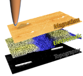
- an MFM probe) as the bias voltage was varied between ±1.5 V. The vertical profiles measured on the Co nanowire (black line) and on the substrate (red line) are shown in Figure 2c. Notice the parabolic dependence of the frequency shift versus voltage, which corresponds to an electrostatic interaction


Formation of precise 2D Au particle arrays via thermally induced dewetting on pre-patterned substrates
Beilstein J. Nanotechnol. 2011, 2, 318–326, doi:10.3762/bjnano.2.37
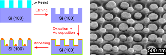
- nanoparticles, due to their wide range of potential applications in plasmonics [1][2], magnetic memories [3], DNA detection [4], and catalysis for nanowire and nanofiber growth [5][6]. Nanoparticle arrays are typically fabricated either by chemical processes based on self-assembly or by lithography based





A collisional model for AFM manipulation of rigid nanoparticles
Beilstein J. Nanotechnol. 2010, 1, 158–162, doi:10.3762/bjnano.1.19
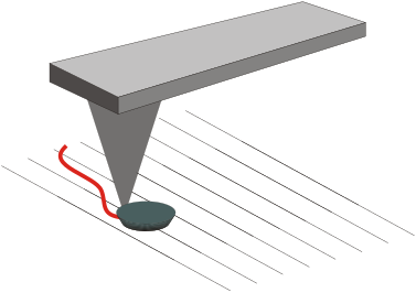
- ] and In the case (b): and In general, both core and cap collisions occur along each scan line and only numerical solutions are possible. However, a complete solution can be found in two important cases: The manipulation of a nanosphere of radius a (L = 0) and that of a thin nanowire of length L (a = 0
- α0 is the impact angle between tip and sphere (with the exception of the very first collision) and is given by In the case of a nanowire, the average direction of motion is well-defined and is given by the simple formula [6] The wire oscillates perpendicularly to this direction: Thus, Equation 7 and
- the force F is directed along the x axis and the total force acting on the particle will be oriented as in tapping mode only if the static friction f can balance the component of F along the island profile. Angle of motion θ of a nanosphere (solid curve) and a nanowire (dashed curve) as a function of


Other Beilstein-Institut Open Science Activities



