


Search results
Search for "defect structure" in Full Text gives 15 result(s) in Beilstein Journal of Nanotechnology.
Influence of an external electric field on the catalytic CO oxidation of nanoscaled CeO2 and its La3+ and Gd3+ congeners
Beilstein J. Nanotechnol. 2026, 17, 1028–1038, doi:10.3762/bjnano.17.70
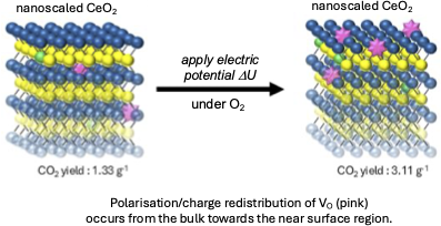
- controlled by the underlying oxidic defect structure. Keywords: cerium oxide; CO oxidation; defect structure; doped cerium oxide; electric potential; Introduction Catalytic CO oxidation is a straightforward approach to reduce CO levels. A variety of catalysts have been synthesized and applied to improve


Materials challenges in solid-state sensors for continuous monitoring of ions in water
Beilstein J. Nanotechnol. 2026, 17, 935–973, doi:10.3762/bjnano.17.66
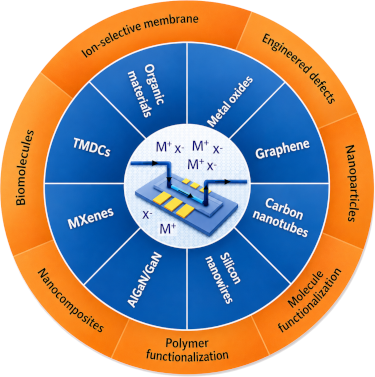
- ) are one-dimensional nanostructures composed of seamless cylinders of sp2-bonded carbon atoms formed by rolling up graphene sheets, with their material properties governed primarily by the number of walls, diameter, chirality, and defect structure. Single-walled carbon nanotubes (SWCNTs) consist of a


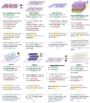
Substrate-dependent pore formation in molybdenum disulfide monolayers under ion irradiation
Beilstein J. Nanotechnol. 2026, 17, 769–780, doi:10.3762/bjnano.17.54
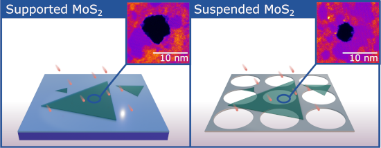
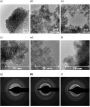
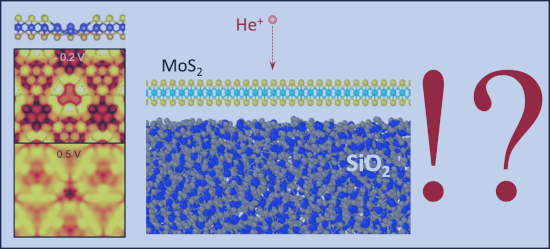
- supported samples that suggested pronounced topographic changes but could not resolve the defect structure [40][41], our STEM analysis shows that irradiation on SiO2 produces well-defined, pore-shaped defects with no obvious long-range lattice distortion of the surrounding material (see Supporting


Upcycling agroindustrial waste into graphene oxide supports for gold nanoparticles: toward sustainable nanomaterials
Beilstein J. Nanotechnol. 2026, 17, 489–504, doi:10.3762/bjnano.17.32
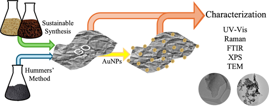
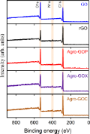
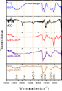
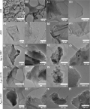
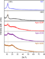
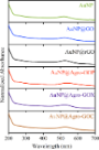
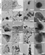
- differences in surface chemistry and defect structure directly govern the photochemical growth of AuNPs, with highly oxidized and functionalized matrices promoting the formation of smaller, well-dispersed nanoparticles. In contrast, less oxidized or more graphitic supports yield larger, more aggregated AuNPs



Defects and defect-mediated engineering of two-dimensional materials: challenges and open questions
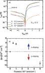
Beilstein J. Nanotechnol. 2026, 17, 454–488, doi:10.3762/bjnano.17.31





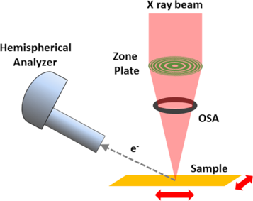
Nanostructured materials characterized by scanning photoelectron spectromicroscopy
Beilstein J. Nanotechnol. 2025, 16, 700–710, doi:10.3762/bjnano.16.54
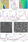
- Ni3+ to reach charge neutrality. Additionally, NiO exhibits a wide bandgap, which also prompts considerable research interest. The properties of NiO are highly dependent on the synthesis method, owing to the variable dimensionality, morphology, crystalline orientation, and defect structure [44


A TiO2@MWCNTs nanocomposite photoanode for solar-driven water splitting
Beilstein J. Nanotechnol. 2022, 13, 1520–1530, doi:10.3762/bjnano.13.125
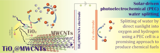
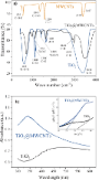
- the Raman spectrum of MWCNTs, there are two bands, that is, the D band at 1324 cm−1 and the G band at 1585 cm−1, which are ascribed to the defect structure and the ordered graphitic structure of the MWCNTs, respectively. The ratio between the D band and G band intensities (ID/IG) of the TiO2@MWCNTs



Effects of temperature and repeat layer spacing on mechanical properties of graphene/polycrystalline copper nanolaminated composites under shear loading
Beilstein J. Nanotechnol. 2021, 12, 863–877, doi:10.3762/bjnano.12.65
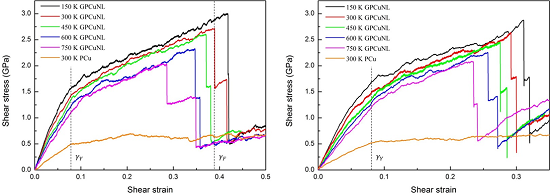
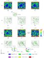
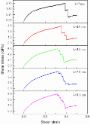
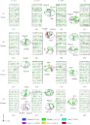
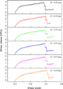
- are rearranged to form a pentagon–heptagon (5–7–7–5) structure, which is known as the Stone–Wales defect structure [40]. It can be seen as the result of a 90° rotation of the C–C bonding, which transfers four hexagons into two pentagons and two heptagons [41][42]. After self-healing, the strength of










Direct observation of the Si(110)-(16×2) surface reconstruction by atomic force microscopy
Beilstein J. Nanotechnol. 2020, 11, 1750–1756, doi:10.3762/bjnano.11.157
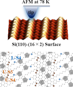
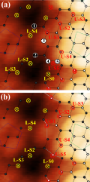
- pentagons actually consisted of five atoms. A non-pentagonal structure in the 16×2 reconstruction and the disorder region were observed with high resolution, and the defect structure of the pentagon due to the lack of a P3 atom in the structure of pentagon was observed. We also observed the atoms of U-S4, U



Hexagonal boron nitride: a review of the emerging material platform for single-photon sources and the spin–photon interface
Beilstein J. Nanotechnol. 2020, 11, 740–769, doi:10.3762/bjnano.11.61





Addition of Zn during the phosphine-based synthesis of indium phospide quantum dots: doping and surface passivation
Beilstein J. Nanotechnol. 2015, 6, 1237–1246, doi:10.3762/bjnano.6.127
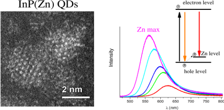
- morphology, size, and defect structure of the nanoparticles as well as the Zn distribution, transmission electron microscopy was applied. The main results of the study are shown in Figure 3, Figure 4 and Figure 5. Figure 3a shows a low-magnification TEM image of non-doped InP QDs and the corresponding


Deformation-induced grain growth and twinning in nanocrystalline palladium thin films
Beilstein J. Nanotechnol. 2013, 4, 554–566, doi:10.3762/bjnano.4.64
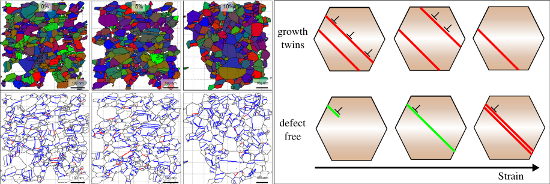
- ., pores and impurities may pin grain boundaries [14][15]. Furthermore, the different production techniques may also lead to different grain boundary structures with varying free volume and defect structure [4][16][17]. All these factors will affect the mechanical behavior of the material, making it


Grain boundaries and coincidence site lattices in the corneal nanonipple structure of the Mourning Cloak butterfly
Beilstein J. Nanotechnol. 2013, 4, 292–299, doi:10.3762/bjnano.4.32
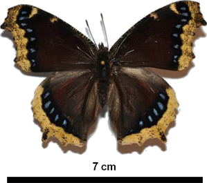
- detail and from a crystallography/defect-structure point of view. The results of this investigation will be published shortly [10]. Briefly, this study has shown that the highly ordered hexagonal structure is made up of nipples with average diameters on the order of 150 nm and a unit cell lattice


Catalytic activity of nanostructured Au: Scale effects versus bimetallic/bifunctional effects in low-temperature CO oxidation on nanoporous Au
Beilstein J. Nanotechnol. 2013, 4, 111–128, doi:10.3762/bjnano.4.13
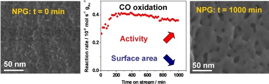
- diffraction peaks and the defect structure of the material [39][42] imply that the contribution of lattice defects/lattice strain to the reflection broadening may not be neglected. Overall, the Scherrer equation is therefore not an appropriate way of determining the ligament size. Nonetheless, the width of


Synthesis and electrical characterization of intrinsic and in situ doped Si nanowires using a novel precursor
Beilstein J. Nanotechnol. 2012, 3, 564–569, doi:10.3762/bjnano.3.65
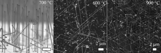
- . To tune the NWs for their respective applications, their electrical and optical properties, which strongly depend on the diameter [8] as well as the crystallographic orientation [9] and defect structure [10] of the NW, must be carefully adjusted. Several synthesis techniques have proven suitable to





