Abstract
The hardware implementation of signal microprocessors based on superconducting technologies seems relevant for a number of niche tasks where performance and energy efficiency are critically important. In this paper, we consider the basic elements for superconducting neural networks on radial basis functions. We examine the static and dynamic activation functions of the proposed neuron. Special attention is paid to tuning the activation functions to a Gaussian form with relatively large amplitude. For the practical implementation of the required tunability, we proposed and investigated heterostructures designed for the implementation of adjustable inductors that consist of superconducting, ferromagnetic, and normal layers.
Introduction
For modern telecommunications, probabilistic identification of various sources in a broadband group signal is extremely important. Also, probabilistic analysis is used in the consideration of stochastic processes [1-4], as a popular machine learning method for spatial interpolation of non-stationary and non-Gaussian data [5], as a central part of a compensation block to enhance the tracking performance in control systems for a class of nonlinear and non-Gaussian stochastic dynamic processes [6].
An important example for this work is the cognitive radio, which is able to receive information about the features of the “radio environment” and adjust its operating parameters based on this data [7-13]. Similar problems arise nowadays when reading data in superconducting noisy intermediate-scale quantum (NISQ) computers [14-17]. Here again, we need real-time identification and classification of varying signals from multiple sources (qubits) in a narrow frequency range. When working with large data, it is necessary to create specialized neural networks at the hardware level to effectively solve such problems.
Josephson digital circuits and analog receivers have been used for a long time to create software-defined radio-systems [18-25] as well as read-out circuits for quantum computing [26-33]. They realize a unique combination of a wide dynamic range and high sensitivity when receiving signals, with high performance and energy efficiency at the stage of the processing. It seems reasonable to implement additional processing of incoming data inside the cryosystem using the capabilities of neural network computing [34-43]. The creation of an extremely low-dissipating element base for such systems is a very actual scientific and technical task, which requires theoretical and experimental studies of the features of macroscopic quantum interference in the complex Josephson circuits.
The direct use of the previously proposed superconducting adiabatic neural network (ANN) based on the perceptron [44-48] for probabilistic identification is not possible. In particular, during the formation of the output signal in the ANN, the so-called global approximation of the input signal is implemented [11,12], in which almost all neurons are included in signal processing. In addition, the perceptron is a fully connected network, which means an abundance of synaptic connections between neurons. These circumstances suppose a highly resource-intensive learning of the network for signal analysis. There is an alternative approach with a representation of the input set of data into the set of output values by using only one hidden layer of neurons. Each of these neurons is responsible for its own area of the parameter space of incoming data. This is the probabilistic or Bayesian approach, where radial basis functions (for example, Gaussian-like functions) are used as neuron activation functions.
The most common networks operating on this principle are radial basis function networks (RBFNs) (also known as Bayesian networks). When using such a network, objects are classified on the basis of assessments of their proximity to neighboring samples. For each sample, a decision can be made based on the selection of the most likely class from those to which the sample could belong. Such a solution requires an estimate of the probability density function for each class. This score is obtained by consideration of training data. The formal rule is that the class with the tightest distribution in the scope of the unknown instance will take precedence over other classes. The traditional approach for estimating the probability density for each class is to assume that the density has some definite form. The normal distribution is the most preferred since it allows one to estimate such parameters of the model as the mean and standard deviation analytically. The superconducting implementation of the key elements of the discussed neural networks is the focus of this work.
Results and Discussion
Model of tunable Gauss-neuron: numerical simulations
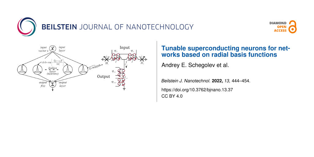
A common architecture of the considered RBFNs [49] is presented in Figure 1a. These networks have only one hidden layer of neurons on which components of the input vector x are fed. Every neuron of the hidden layer calculates the values of the 1D function hk(x).
![[2190-4286-13-37-i1]](/bjnano/content/inline/2190-4286-13-37-i1.svg?max-width=590&scale=1.18182)
where xk is the k-th reference point and σk is the scattering parameter for the one-dimensional function ![[Graphic 1]](/bjnano/content/inline/2190-4286-13-37-i16.svg?max-width=637&scale=1.18182) .
.
![[2190-4286-13-37-1]](/bjnano/content/figures/2190-4286-13-37-1.png?scale=2.0&max-width=1024&background=FFFFFF)
Figure 1: (a) Schematic illustration of a RBF network. (b) Schematic representation of a Gauss-neuron ensuring a Gauss-like transfer function.
Figure 1: (a) Schematic illustration of a RBF network. (b) Schematic representation of a Gauss-neuron ensurin...
In this paper, we propose a modified tunable neuron circuit [44] for RBFNs (see Figure 1b), with a Gaussian-like activation function. It consists of two identical Josephson junctions JJ1 and JJ2 in the shoulders with input inductances, L, and output inductance Lout. It is also used to set an additional bias magnetic flux, Φb. Flux biasing is used to provide a suitable transfer function for asynchronous circulation of currents in the connected circuits. In the following, we will call such a cell a “Gauss-neuron” or a “G-cell/neuron”.
Hereinafter, we use normalized values for typical parameters of the circuit. All fluxes (input Φin and output Φout, and bias Φb) are normalized to the flux quantum Φ0; currents are normalized to the critical current of the Josephson junctions IC; inductances are normalized to the characteristic inductance 2πLIC/Φ0, times are normalised to the characteristic time tC = Φ0/(2πVC) (VC is the characteristic voltage of a Josephson junction). Equations of motion were obtained in terms of half-sum and half-difference of Josephson phases φ1, φ2 (θ = (φ1 + φ2)/2 and ψ = (φ1 − φ2)/2), a detailed derivation of the equations is given in the Appendix section:
![[2190-4286-13-37-i2]](/bjnano/content/inline/2190-4286-13-37-i2.svg?max-width=590&scale=1.18182)
![[2190-4286-13-37-i3]](/bjnano/content/inline/2190-4286-13-37-i3.svg?max-width=590&scale=1.18182)
The output magnetic flux obeys the following equation:
![[2190-4286-13-37-i4]](/bjnano/content/inline/2190-4286-13-37-i4.svg?max-width=590&scale=1.18182)
Figure 2a,b shows the families of transfer functions of a Gauss-neuron at different bias fluxes. They are compared with the radial basis function taken in the form g(x) = exp(−x2/(2σ2)) (dashed line). All transfer functions were normalized to their maximum value, since at the first stage we were interested in the shape of the curve itself. It can be seen that the shape of the response meets the requirements; in addition, it can be adjusted using a bias magnetic flux φb. An important feature of the system is that it also allows for non-volatile tuning with memory using tunable inductances l and lout, see Figure 2c–e. Estimations for different values of φb show that the best match (with Gauss-like radial basis function) can be achieved with φb = 0.05π and inductance values of l = 0.1 and lout = 0.1. Also the investigation of the full width at half maximum (FWHM) and of the amplitude of the transfer functions of the Gauss-neuron was carried out for different values of φb (Figure 2c,d) and inductance l (Figure 2e). It can be seen that an increase in the value of the inductance l decreases the FWHM of the transfer function and increases its amplitude. The bias flux is a convenient adjustment of the transfer function of the tunable Gauss-neuron; the bias flux should vary in the [0…0.5]π range to save the proper form of the transfer function. The mean of the transfer function can be controlled by an additional constant component in the input flux. By selecting the parameters of a configurable G-neuron, we can make the effective field period for the activation function (resulting from the Φ0-periodicity of all flux dependencies for the interferometer-based structures) large enough for practical use in real neural networks (Figure 2e).
![[2190-4286-13-37-2]](/bjnano/content/figures/2190-4286-13-37-2.png?scale=2.0&max-width=1024&background=FFFFFF)
Figure 2: Transfer functions (normalized) and their main characteristics for the Gauss-neuron. (a, b) Families of the normalised transfer functions depending on the magnitude of the bias flux φb for various pairs of inductances l and lout: (a) l = 0.1, lout = 0.1; (b) l = 0.9, lout = 0.1. (c) Dependencies of FWHM and amplitude on the bias flux φb of transfer functions for l = 0.1, 0.5, and 0.9 with lout = 0.1. (d) Dependencies of FWHM and amplitude on the inductance l for transfer functions of the Gauss-neuron at lout = 0.1 and φb = 0.05π.
Figure 2: Transfer functions (normalized) and their main characteristics for the Gauss-neuron. (a, b) Familie...
We calculated the standard deviation (SD) of the transfer function from the Gaussian-like function g(x) with fixed amplitude. The obtained results are presented in the {l, lout} plane. This visualization allows one to find the most proper operating parameters for the considered element. The magnitude of the amplitude of the transfer function is also presented (Figure 3a,b). The optimal values of inductance corresponding to the minimum of SD lies in the hollow of the surface, see Figure 3b. The minimum SD value is reached at l = 0.1, lout = 0.1. The position of the hollow in Figure 3b could be expressed as (lout)SD ≈ 0.8 − 0.55(l)SD. At the same time, for relatively small φb, the transfer function amplitude increases with increase of the output and shoulder inductances, lout and l. Thus, the choice between the proximity of the transfer function to a Gaussian-like form and the maximization of the response amplitude is determined by the specifics of the network when solving a specific problem. Once again, we emphasize that variations in the parameters of the circuit within a fairly wide range allow one to change the amplitude and width of the activation function, while maintaining its Gaussian-like shape.
![[2190-4286-13-37-3]](/bjnano/content/figures/2190-4286-13-37-3.png?scale=2.0&max-width=1024&background=FFFFFF)
Figure 3: (a) Amplitude of the transfer function and (b) its standard deviation from the Gaussian-like function depending on the inductances l and lout of the G-cell. The bias flux is equal to 0.05π.
Figure 3: (a) Amplitude of the transfer function and (b) its standard deviation from the Gaussian-like functi...
The dynamic transfer functions (i.e., the dependencies of the output current on the time-varying input flux) were also calculated, see Figure 4a. The input magnetic signal is a smoothed trapezoidal function of time with a rise/fall time tRF, see the inset in Figure 4b. It can be seen that the dynamic activation function of the required type without hysteresis can be obtained with adiabatic operation of the cell (tRF up to 8000tC, where tC is the characteristic time for the Josephson junction). The dissipation during the operation of the Gauss-neuron remains small, which justifies classifying the proposed cell as adiabatic (Figure 4b).
![[2190-4286-13-37-4]](/bjnano/content/figures/2190-4286-13-37-4.png?scale=2.0&max-width=1024&background=FFFFFF)
Figure 4: (a) Dynamic transfer function of a Gauss-neuron for a trapezoidal external signal for different values of the rise/fall times of the signal tRF and (b) energy dissipation, normalised to the characteristic energy E0 = Φ0IC/2π, as function of the rise/fall time of the input signal for different bias fluxes: φb = {0.01, 0.05, 0.1}π. The insert demonstrates the form of temporal dynamic for input flux and dissipation. If the critical current for Josephson junctions IC is equal to 100 μA and φb = 0.05π than Edis ≈ 0.01 aJ for tRF = 6 ns (corresponds to approx. 1700tC).
Figure 4: (a) Dynamic transfer function of a Gauss-neuron for a trapezoidal external signal for different val...
Realization of tunability: adjustable kinetic inductance
For neural networks based on the considered G-neurons, tunable elements with linear current-to-flux transformation (linear inductors) and memory properties are extremely important [50,51]. Tunability of the inductance l in Figure 1b allows for an in situ switching between operating modes directly on the chip.
In thin layers of superconductors used to create parts of a neuron, the kinetic inductance is relatively large compared to the geometric one [52]. This is important for us since one can change the kinetic inductance relatively simply by controlling the concentration of superconducting charge carriers (Cooper pairs or superconducting correlations). This approach is the basis of the concept of our tunable in situ Gauss-neuron. A similar idea is used in kinetic inductance devices, which are based on thin superconducting strips [53,54]. They are commonly used for the design of photon detectors and parametric amplifiers. But these devices use nonlinear properties of thin superconducting films at large values of carrying currents comparable to the critical current. However, for our purposes, linear inductors are required. So we consider only the case of a small current in comparison with the depairing current of the superconductor.
In this paper, we propose a tunable kinetic inductance with integrated spin-valve structure [46]. A superconducting spin valve is a device that can control the propagation of the superconducting charge carriers, induced from the superconducting layer via the proximity effect. The typical spin valve [55-57] is a hybrid structure containing at least a pair of ferromagnetic (FM) layers with different coercive forces. Variations in the relative orientation of their magnetizations change the spatial distribution of the superconducting order parameter. In the case of parallel magnetization of the FM layers the Cooper pairs are effectively depairing inside them (closed spin valve). For the antiparallel orientation, the effective exchange energy of the magnetic layers is averaged and suppression of the superconducting order parameter is weaker (open spin valve), providing a propagation of Cooper pairs to the outlying layers of the hybrid structure. The switching between the open and closed states of the valve leads to a noticeable change in the spatial distribution of Cooper pairs. The implementation of a thin superconducting spacer (s) between the FM layers supports the superconducting order parameter and increases the efficiency of the spin valve effect [58]. Here, we propose a development of this approach, allowing one to significantly increase the effective variations in the kinetic inductance.
We study proximity effect and electronic transport in the multilayer hybrid structures in the frame of Usadel equations [59]:
![[2190-4286-13-37-i5]](/bjnano/content/inline/2190-4286-13-37-i5.svg?max-width=590&scale=1.18182)
![[2190-4286-13-37-i6]](/bjnano/content/inline/2190-4286-13-37-i6.svg?max-width=590&scale=1.18182)
with Kupriyanov–Lukichev boundary conditions [60],
![[2190-4286-13-37-i7]](/bjnano/content/inline/2190-4286-13-37-i7.svg?max-width=590&scale=1.18182)
at the S/FM interfaces. Here G and F are normal and anomalous Green's functions, Δ is a pair potential (superconducting order parameter), ω = πkBT (2n + 1), where n is a natural number, T is the temperature, kB is Boltzmann’s constant, ![[Graphic 2]](/bjnano/content/inline/2190-4286-13-37-i17.svg?max-width=637&scale=1.18182) where H is the exchange energy (H = 0 in S and N layers). The indexes “l” and “r” denote the materials at, respectively, the left and right side of an interface, ξ is the coherence length, ρ is the resistivity of the material (in the following, ξ and ρ will also will be mentioned with indexes that denote the layer of these parameters), TC is the critical temperature of the superconductor, and γB = (RBA)/(ρlξl) is the interface parameter, where RBA is the resistance per square of the interface
where H is the exchange energy (H = 0 in S and N layers). The indexes “l” and “r” denote the materials at, respectively, the left and right side of an interface, ξ is the coherence length, ρ is the resistivity of the material (in the following, ξ and ρ will also will be mentioned with indexes that denote the layer of these parameters), TC is the critical temperature of the superconductor, and γB = (RBA)/(ρlξl) is the interface parameter, where RBA is the resistance per square of the interface
The calculated distribution of the anomalous Green function, F, permits one to estimate the ability to influence the propagation of the superconducting correlations (screening properties) for the hybrid structure. The spatial distribution of the screening length λ(x) directly depends on the proximization of the superconducting order parameter in the system [61,62]:
![[2190-4286-13-37-i8]](/bjnano/content/inline/2190-4286-13-37-i8.svg?max-width=590&scale=1.18182)
where ρS is the resistivity of the superconducting material, μ0 is the vacuum permeability and ℏ is Planck’s constant. For instance, for a homogeneous niobium film, the estimate for the constant λ0 is around 100 nm, while experimentally measured values of the screening length λ at T = 4.2 K are around 150 nm. The expression for the kinetic inductance of the structure is directly correlated with screening length [52,63],
![[2190-4286-13-37-i9]](/bjnano/content/inline/2190-4286-13-37-i9.svg?max-width=590&scale=1.18182)
where X is the length of the strip, W is the width, and d is the thickness of the multilayer. In our calculations, we assume that the currents in the system are weak, and the structure thickness is much smaller than the screening length.
We propose a hybrid structure (see Figure 5) consisting of three parts, namely a pairing source, a spin valve, and a current-carrying layer of normal metal with low-resistivity. The general principle of operation is the following: The pairing source generates Cooper pairs and the spin valve controls their propagation to the layer von low inductance. If the valve is open (Figure 5b), the normal metal is repleted with Cooper pairs, and the biggest part of the supercurrent IS is flowing along the structure through the metallic layer (N) with relatively low inductance. In the case of the closed valve (Figure 5a), pairs are locked up in the source layer, and the supercurrent IS is limited to this highly inductive part of the structure. The redistribution of the current flowing along the multilayer is associated with a change of the total kinetic inductance.
![[2190-4286-13-37-5]](/bjnano/content/figures/2190-4286-13-37-5.png?scale=2.0&max-width=1024&background=FFFFFF)
Figure 5: Sketch of the tunable kinetic inductance based on multilayer structure in the (a) closed and (b) open states. Blue solid arrows reveal magnetization orientation of FM1 and FM2 layers, and dashed yellow arrows demonstrate direction and localization of the supercurrent IS.
Figure 5: Sketch of the tunable kinetic inductance based on multilayer structure in the (a) closed and (b) op...
For a quantitative model, we choose the following components of the structure: The pairing source is a superconductor layer slightly thicker than the critical value at which the pair potential appears. During calculations we suppose its thickness dS = 3ξS.
The spin valve can be implemented as a multilayer structure FM1–s–FM2–s–FM1–s–FM2 with several ferromagnetic layers FM1 and FM2 of different thicknesses dFM1,2 (dFM1 = 0.15ξ, dFM2 = 0.1ξ, exchange energy H = 100 kBTC in calculations, separated by thin spacers of a superconductor or normal metal (N) (ds = 0.5ξ for example).
The control of the spin valve is operated by turning the FM layers into states with parallel (P) and antiparallel (AP) mutual orientations of their magnetizations. This process can be realized by application of the finite external magnetic field or by injection of the spin current due to the spin torque effect [56]. For the proposed design of the Gauss-neuron, it is suitable to change magnetizations in the tunable inductance l with the control currents in the input circuits, see Figure 1b. Earlier we experimentally demonstrated [58] that for such a control it is sufficient to create a magnetic field strength of the order of 30 Oe. Note that after the control current is turned off, the valve remains in the open/closed state, since the direction of magnetizations in the FM layers is preserved.
The current-carrying layer is a thin strip of normal metal with thickness dN = 2ξ and small resistivity ρN ≪ ρS, which ensures its lower kinetic inductance relative to the rest of the structure. This leads to a flow of the current mostly through this layer in the case of the open valve.
Figure 6a shows the spatial distributions of the pairing amplitude F(x) in the cross section of this structure for parallel (blue solid line) and antiparallel (red dashed line) orientations of the magnetization of the FM1 and FM2 layers. The pairing amplitude F significantly drops in the spin valve region for both cases. However, the residual level of proximization (value of F) in the N layer is five times larger for the AP orientation than for the P orientation.
![[2190-4286-13-37-6]](/bjnano/content/figures/2190-4286-13-37-6.png?scale=2.0&max-width=1024&background=FFFFFF)
Figure 6: Spatial distribution of the pair amplitude F in the hybrid structures (a) S–FM1–s–FM2–s–FM1–s–FM2–N without additional s1 layer and (b) S–FM1–s–FM2–s–FM1–s–FM2–s1–N with an additional superconducting layer for parallel (blue solid line) and antiparallel (red dashed line) mutual orientations of magnetization between FM1 and FM2 layers.
Figure 6: Spatial distribution of the pair amplitude F in the hybrid structures (a) S–FM1–s–FM2–s–FM1–s–FM2–N...
To enhance the effect, we propose to add an additional superconductor layer s1 (Figure 6b). In the case of the closed valve, the s1 layer is in the normal state, and the superconducting correlations in the N layer are negligible. If the valve is open, the s1 layer goes into a superconducting state with an increase of the pairing amplitude F in the N layer up to two times (see Figure 6a).
Figure 7 demonstrates the dependence of the kinetic inductance of the structure shown in Figure 6b versus as a function of the thickness of the intermediate s or n layers. At large thicknesses of the intermediate layers, the valve loses efficiency. In the case of normal spacers, the transition occurs to a completely normal state, where the kinetic inductance of the entire structure coincides with the kinetic inductance of the source layer S. With a large thickness of superconducting spacers s, the valve system also loses efficiency, transferring the entire structure to a completely superconducting state. However, at thicknesses of the order of (0.5…1)ξ, the maximum spin-valve effect appears, and the total kinetic inductance of the structure changes several times during switching between states with parallel and antiparallel magnetization orientations.
![[2190-4286-13-37-7]](/bjnano/content/figures/2190-4286-13-37-7.png?scale=2.0&max-width=1024&background=FFFFFF)
Figure 7: Kinetic inductance of the hybrid structures S–FM1–s–FM2–s–FM1–s–FM2–s–N and S–FM1–n–FM2–n–FM1–n–FM2–s1–N for parallel (dark blue solid line and long dashed green line) and antiparallel (red dashed line and orange dash–dot line) mutual orientations of magnetization between FM1 and FM2 layers as functions of the spacer thickness.
Figure 7: Kinetic inductance of the hybrid structures S–FM1–s–FM2–s–FM1–s–FM2–s–N and S–FM1–n–FM2–n–FM1–n–FM2...
We also made some estimates for the quantitative value of the kinetic inductance of the structure shown in Figure 7 based on niobium technology. The inductance of the strip with width W = 100 nm, length X = 1 μm, and total thickness d = 80 nm (this corresponds to the spacer thickness ds =5 nm) the estimated kinetic inductance is about 7 pH in the closed state and about 15 pH in the open state. For comparison, the geometric inductance of such a strip is of the order of 1 pH.
Conclusion
We have considered a basic cell for superconducting signal neurocomputers designed for the fast processing of a group signal with extremely low energy dissipation. It turned out that for this purpose it is possible to modify the previously discussed element of adiabatic superconducting neural networks. The ability to adjust the parameters of the studied Gauss-cell (with Gaussian-like activation function) is very important for in situ switching between operating modes. Using microscopic modeling, we have shown that the desired compact tunable passive element can be implemented in the form of a controllable kinetic inductance. An example is a multilayer structure consisting of a superconducting “source”, a current-carrying layer and a spin valve with at least two magnetic layers with different thicknesses. The proposed tunable inductance does not require suppression of superconductivity in the source layer. In this case, the spin-valve effect determines the efficiency of penetration of superconducting correlations into the current-carrying layer, which is the reason for the change in inductance.
Appendix
We present the derivation of Equation 2–Equation 4 in the framework of the resistively shunted junction (RSJ) model. A typical approach to obtain the equations of motion for Josephson systems is to write the Kirchhoff and phase constraints. From Figure 1b), it follows:
![[2190-4286-13-37-i10]](/bjnano/content/inline/2190-4286-13-37-i10.svg?max-width=590&scale=1.18182)
Let us sum up the second and third equations of the system in Equation 10, taking into account the first equation, and dividing the left and right sides by 2:
![[2190-4286-13-37-i11]](/bjnano/content/inline/2190-4286-13-37-i11.svg?max-width=590&scale=1.18182)
As the current through the Josephson junction has a form ![[Graphic 3]](/bjnano/content/inline/2190-4286-13-37-i18.svg?max-width=637&scale=1.18182) , Equation 11 gives us the first equation of motion (Equation 2) for the Gauss-neuron:
, Equation 11 gives us the first equation of motion (Equation 2) for the Gauss-neuron:
![[2190-4286-13-37-i12]](/bjnano/content/inline/2190-4286-13-37-i12.svg?max-width=590&scale=1.18182)
Similar operations should be conducted for the difference between the second and third equations of the system in Equation 10:
![[2190-4286-13-37-i13]](/bjnano/content/inline/2190-4286-13-37-i13.svg?max-width=590&scale=1.18182)
and the second equation of motion (Equation 3) for the system is obtained:
![[2190-4286-13-37-i14]](/bjnano/content/inline/2190-4286-13-37-i14.svg?max-width=590&scale=1.18182)
To obtain Equation 4, we have to convert Equation 11 according to the expression i1 + i2 = −iout = −(φout/lout):
![[2190-4286-13-37-i15]](/bjnano/content/inline/2190-4286-13-37-i15.svg?max-width=590&scale=1.18182)
References
-
Turchetti, C.; Crippa, P.; Pirani, M.; Biagetti, G. IEEE Trans. Neural Networks 2008, 19, 1033–1060. doi:10.1109/tnn.2007.2000055
Return to citation in text: [1] -
Groth, C.; Costa, E.; Biancolini, M. E. Aircr. Eng. Aerosp. Technol. 2019, 91, 620–633. doi:10.1108/aeat-07-2018-0178
Return to citation in text: [1] -
Zhang, J.; Li, H.; Hu, B.; Min, Y.; Chen, Q.; Hou, G.; Huang, C. Modelling of SFR for Wind-Thermal Power Systems via Improved RBF Neural Networks. In CISC 2020: Proceedings of 2020 Chinese Intelligent Systems Conference, 2020; pp 630–640.
Return to citation in text: [1] -
Xie, S.; Xie, Y.; Huang, T.; Gui, W.; Yang, C. IEEE Trans. Ind. Electron. 2019, 66, 1192–1202. doi:10.1109/tie.2018.2835402
Return to citation in text: [1] -
Shi, C.; Wang, Y. Geosci. Front. 2021, 12, 339–350. doi:10.1016/j.gsf.2020.01.011
Return to citation in text: [1] -
Zhou, Y.; Wang, A.; Zhou, P.; Wang, H.; Chai, T. Automatica 2020, 112, 108693. doi:10.1016/j.automatica.2019.108693
Return to citation in text: [1] -
Abidi, A. A. IEEE J. Solid-State Circuits 2007, 42, 954–966. doi:10.1109/jssc.2007.894307
Return to citation in text: [1] -
Ulversoy, T. IEEE Commun. Surv. Tutorials 2010, 12, 531–550. doi:10.1109/surv.2010.032910.00019
Return to citation in text: [1] -
Wang, B.; Liu, K. J. R. IEEE J. Sel. Top. Signal Process. 2011, 5, 5–23. doi:10.1109/jstsp.2010.2093210
Return to citation in text: [1] -
Macedo, D. F.; Guedes, D.; Vieira, L. F. M.; Vieira, M. A. M.; Nogueira, M. IEEE Commun. Surv. Tutorials 2015, 17, 1102–1125. doi:10.1109/comst.2015.2402617
Return to citation in text: [1] -
Adjemov, S. S.; Klenov, N. V.; Tereshonok, M. V.; Chirov, D. S. Moscow Univ. Phys. Bull. (Engl. Transl.) 2015, 70, 448–456. doi:10.3103/s0027134915060028
Return to citation in text: [1] [2] -
Adjemov, S. S.; Klenov, N. V.; Tereshonok, M. V.; Chirov, D. S. Program. Comput. Software 2016, 42, 121–128. doi:10.1134/s0361768816030026
Return to citation in text: [1] [2] -
Ahmad, W. S. H. M. W.; Radzi, N. A. M.; Samidi, F. S.; Ismail, A.; Abdullah, F.; Jamaludin, M. Z.; Zakaria, M. N. IEEE Access 2020, 8, 14460–14488. doi:10.1109/access.2020.2966271
Return to citation in text: [1] -
Córcoles, A. D.; Magesan, E.; Srinivasan, S. J.; Cross, A. W.; Steffen, M.; Gambetta, J. M.; Chow, J. M. Nat. Commun. 2015, 6, 6979. doi:10.1038/ncomms7979
Return to citation in text: [1] -
Arute, F.; Arya, K.; Babbush, R.; Bacon, D.; Bardin, J. C.; Barends, R.; Biswas, R.; Boixo, S.; Brandao, F. G. S. L.; Buell, D. A.; Burkett, B.; Chen, Y.; Chen, Z.; Chiaro, B.; Collins, R.; Courtney, W.; Dunsworth, A.; Farhi, E.; Foxen, B.; Fowler, A.; Gidney, C.; Giustina, M.; Graff, R.; Guerin, K.; Habegger, S.; Harrigan, M. P.; Hartmann, M. J.; Ho, A.; Hoffmann, M.; Huang, T.; Humble, T. S.; Isakov, S. V.; Jeffrey, E.; Jiang, Z.; Kafri, D.; Kechedzhi, K.; Kelly, J.; Klimov, P. V.; Knysh, S.; Korotkov, A.; Kostritsa, F.; Landhuis, D.; Lindmark, M.; Lucero, E.; Lyakh, D.; Mandrà, S.; McClean, J. R.; McEwen, M.; Megrant, A.; Mi, X.; Michielsen, K.; Mohseni, M.; Mutus, J.; Naaman, O.; Neeley, M.; Neill, C.; Niu, M. Y.; Ostby, E.; Petukhov, A.; Platt, J. C.; Quintana, C.; Rieffel, E. G.; Roushan, P.; Rubin, N. C.; Sank, D.; Satzinger, K. J.; Smelyanskiy, V.; Sung, K. J.; Trevithick, M. D.; Vainsencher, A.; Villalonga, B.; White, T.; Yao, Z. J.; Yeh, P.; Zalcman, A.; Neven, H.; Martinis, J. M. Nature 2019, 574, 505–510. doi:10.1038/s41586-019-1666-5
Return to citation in text: [1] -
Babukhin, D. V.; Zhukov, A. A.; Pogosov, W. V. Phys. Rev. A 2020, 101, 052337. doi:10.1103/physreva.101.052337
Return to citation in text: [1] -
Vozhakov, V.; Bastrakova, M. V.; Klenov, N. V.; Soloviev, I. I.; Pogosov, W. V.; Babukhin, D. V.; Zhukov, A. A.; Satanin, A. M. Phys.-Usp. 2022, in press. doi:10.3367/ufne.2021.02.038934
Return to citation in text: [1] -
Fujimaki, A.; Katayama, M.; Hayakawa, H.; Ogawa, A. Supercond. Sci. Technol. 1999, 12, 708–710. doi:10.1088/0953-2048/12/11/305
Return to citation in text: [1] -
Fujimaki, A.; Nakazono, K.; Hasegawa, H.; Sato, T.; Akahori, A.; Takeuchi, N.; Furuta, F.; Katayama, M.; Hayakawa, H. IEEE Trans. Appl. Supercond. 2001, 11, 318–321. doi:10.1109/77.919347
Return to citation in text: [1] -
Brock, D. K.; Mukhanov, O. A.; Rosa, J. IEEE Commun. Mag. 2001, 39, 174–179. doi:10.1109/35.900649
Return to citation in text: [1] -
Vernik, I. V.; Kirichenko, D. E.; Filippov, T. V.; Talalaevskii, A.; Sahu, A.; Inamdar, A.; Kirichenko, A. F.; Gupta, D.; Mukhanov, O. A. IEEE Trans. Appl. Supercond. 2007, 17, 442–445. doi:10.1109/tasc.2007.898613
Return to citation in text: [1] -
Gupta, D.; Filippov, T. V.; Kirichenko, A. F.; Kirichenko, D. E.; Vernik, I. V.; Sahu, A.; Sarwana, S.; Shevchenko, P.; Talalaevskii, A.; Mukhanov, O. A. IEEE Trans. Appl. Supercond. 2007, 17, 430–437. doi:10.1109/tasc.2007.898255
Return to citation in text: [1] -
Gupta, D.; Kirichenko, D. E.; Dotsenko, V. V.; Miller, R.; Sarwana, S.; Talalaevskii, A.; Delmas, J.; Webber, R. J.; Govorkov, S.; Kirichenko, A. F.; Vernik, I. V.; Tang, J. IEEE Trans. Appl. Supercond. 2011, 21, 883–890. doi:10.1109/tasc.2010.2095399
Return to citation in text: [1] -
Kornev, V. K.; Soloviev, I. I.; Sharafiev, A. V.; Klenov, N. V.; Mukhanov, O. A. IEEE Trans. Appl. Supercond. 2013, 23, 1800405. doi:10.1109/tasc.2012.2232691
Return to citation in text: [1] -
Mukhanov, O.; Prokopenko, G.; Romanofsky, R. IEEE Microwave Mag. 2014, 15, 57–65. doi:10.1109/mmm.2014.2332421
Return to citation in text: [1] -
Pankratov, A. L.; Gordeeva, A. V.; Kuzmin, L. S. Phys. Rev. Lett. 2012, 109, 087003. doi:10.1103/physrevlett.109.087003
Return to citation in text: [1] -
Soloviev, I. I.; Klenov, N. V.; Pankratov, A. L.; Il'ichev, E.; Kuzmin, L. S. Phys. Rev. E 2013, 87, 060901. doi:10.1103/physreve.87.060901
Return to citation in text: [1] -
Soloviev, I. I.; Klenov, N. V.; Bakurskiy, S. V.; Pankratov, A. L.; Kuzmin, L. S. Appl. Phys. Lett. 2014, 105, 202602. doi:10.1063/1.4902327
Return to citation in text: [1] -
Soloviev, I. I.; Klenov, N. V.; Pankratov, A. L.; Revin, L. S.; Il'ichev, E.; Kuzmin, L. S. Phys. Rev. B 2015, 92, 014516. doi:10.1103/physrevb.92.014516
Return to citation in text: [1] -
McDermott, R.; Vavilov, M. G.; Plourde, B. L. T.; Wilhelm, F. K.; Liebermann, P. J.; Mukhanov, O. A.; Ohki, T. A. Quantum Sci. Technol. 2018, 3, 024004. doi:10.1088/2058-9565/aaa3a0
Return to citation in text: [1] -
Opremcak, A.; Pechenezhskiy, I. V.; Howington, C.; Christensen, B. G.; Beck, M. A.; Leonard, E., Jr.; Suttle, J.; Wilen, C.; Nesterov, K. N.; Ribeill, G. J.; Thorbeck, T.; Schlenker, F.; Vavilov, M. G.; Plourde, B. L. T.; McDermott, R. Science 2018, 361, 1239–1242. doi:10.1126/science.aat4625
Return to citation in text: [1] -
Howington, C.; Opremcak, A.; McDermott, R.; Kirichenko, A.; Mukhanov, O. A.; Plourde, B. L. T. IEEE Trans. Appl. Supercond. 2019, 29, 1700305. doi:10.1109/tasc.2019.2908884
Return to citation in text: [1] -
Leonard, E., Jr.; Beck, M. A.; Nelson, J.; Christensen, B. G.; Thorbeck, T.; Howington, C.; Opremcak, A.; Pechenezhskiy, I. V.; Dodge, K.; Dupuis, N. P.; Hutchings, M. D.; Ku, J.; Schlenker, F.; Suttle, J.; Wilen, C.; Zhu, S.; Vavilov, M. G.; Plourde, B. L. T.; McDermott, R. Phys. Rev. Appl. 2019, 11, 014009. doi:10.1103/physrevapplied.11.014009
Return to citation in text: [1] -
Chiarello, F.; Carelli, P.; Castellano, M. G.; Torrioli, G. Supercond. Sci. Technol. 2013, 26, 125009. doi:10.1088/0953-2048/26/12/125009
Return to citation in text: [1] -
Segall, K.; LeGro, M.; Kaplan, S.; Svitelskiy, O.; Khadka, S.; Crotty, P.; Schult, D. Phys. Rev. E 2017, 95, 032220. doi:10.1103/physreve.95.032220
Return to citation in text: [1] -
Schneider, M. L.; Donnelly, C. A.; Russek, S. E.; Baek, B.; Pufall, M. R.; Hopkins, P. F.; Dresselhaus, P. D.; Benz, S. P.; Rippard, W. H. Sci. Adv. 2018, 4, e1701329. doi:10.1126/sciadv.1701329
Return to citation in text: [1] -
Shainline, J. M.; Buckley, S. M.; McCaughan, A. N.; Chiles, J.; Jafari-Salim, A.; Mirin, R. P.; Nam, S. W. J. Appl. Phys. 2018, 124, 152130. doi:10.1063/1.5038031
Return to citation in text: [1] -
Shainline, J. M.; Buckley, S. M.; McCaughan, A. N.; Chiles, J. T.; Jafari Salim, A.; Castellanos-Beltran, M.; Donnelly, C. A.; Schneider, M. L.; Mirin, R. P.; Nam, S. W. J. Appl. Phys. 2019, 126, 044902. doi:10.1063/1.5096403
Return to citation in text: [1] -
Cheng, R.; Goteti, U. S.; Hamilton, M. C. IEEE Trans. Appl. Supercond. 2019, 29, 1300505. doi:10.1109/tasc.2019.2892111
Return to citation in text: [1] -
Toomey, E.; Segall, K.; Berggren, K. K. Front. Neurosci. 2019, 13, 933. doi:10.3389/fnins.2019.00933
Return to citation in text: [1] -
Toomey, E.; Segall, K.; Castellani, M.; Colangelo, M.; Lynch, N.; Berggren, K. K. Nano Lett. 2020, 20, 8059–8066. doi:10.1021/acs.nanolett.0c03057
Return to citation in text: [1] -
Ishida, K.; Byun, I.; Nagaoka, I.; Fukumitsu, K.; Tanaka, M.; Kawakami, S.; Tanimoto, T.; Ono, T.; Kim, J.; Inoue, K. IEEE Micro 2021, 41, 19–26. doi:10.1109/mm.2021.3070488
Return to citation in text: [1] -
Feldhoff, F.; Toepfer, H. IEEE Trans. Appl. Supercond. 2021, 31, 1800505. doi:10.1109/tasc.2021.3063212
Return to citation in text: [1] -
Schegolev, A. E.; Klenov, N. V.; Soloviev, I. I.; Tereshonok, M. V. Beilstein J. Nanotechnol. 2016, 7, 1397–1403. doi:10.3762/bjnano.7.130
Return to citation in text: [1] [2] -
Soloviev, I. I.; Schegolev, A. E.; Klenov, N. V.; Bakurskiy, S. V.; Kupriyanov, M. Y.; Tereshonok, M. V.; Shadrin, A. V.; Stolyarov, V. S.; Golubov, A. A. J. Appl. Phys. 2018, 124, 152113. doi:10.1063/1.5042147
Return to citation in text: [1] -
Bakurskiy, S.; Kupriyanov, M.; Klenov, N. V.; Soloviev, I.; Schegolev, A.; Morari, R.; Khaydukov, Y.; Sidorenko, A. S. Beilstein J. Nanotechnol. 2020, 11, 1336–1345. doi:10.3762/bjnano.11.118
Return to citation in text: [1] [2] -
Schegolev, A.; Klenov, N.; Soloviev, I.; Tereshonok, M. Supercond. Sci. Technol. 2021, 34, 015006. doi:10.1088/1361-6668/abc569
Return to citation in text: [1] -
Schneider, M.; Toomey, E.; Rowlands, G.; Shainline, J.; Tschirhart, P.; Segall, K. Supercond. Sci. Technol. 2022, 35, 053001. doi:10.1088/1361-6668/ac4cd2
Return to citation in text: [1] -
Park, J.; Sandberg, I. W. Neural Comput. 1991, 3, 246–257. doi:10.1162/neco.1991.3.2.246
Return to citation in text: [1] -
Splitthoff, L. J.; Bargerbos, A.; Grünhaupt, L.; Pita-Vidal, M.; Wesdorp, J. J.; Liu, Y.; Kou, A.; Andersen, C. K.; van Heck, B. arXiv 2022, No. 2202.08729. doi:10.48550/arxiv.2202.08729
Return to citation in text: [1] -
Jué, E.; Iankevich, G.; Reisinger, T.; Hahn, H.; Provenzano, V.; Pufall, M. R.; Haygood, I. W.; Rippard, W. H.; Schneider, M. L. J. Appl. Phys. 2022, 131, 073902. doi:10.1063/5.0080841
Return to citation in text: [1] -
Annunziata, A. J. Single-photon detection, kinetic inductance, and non-equilibrium dynamics in niobium and niobium nitride superconducting nanowires. Ph.D. Thesis, Yale University, New Haven, CT, USA, 2010.
Return to citation in text: [1] [2] -
Annunziata, A. J.; Santavicca, D. F.; Frunzio, L.; Catelani, G.; Rooks, M. J.; Frydman, A.; Prober, D. E. Nanotechnology 2010, 21, 445202. doi:10.1088/0957-4484/21/44/445202
Return to citation in text: [1] -
Bockstiegel, C.; Wang, Y.; Vissers, M. R.; Wei, L. F.; Chaudhuri, S.; Hubmayr, J.; Gao, J. Appl. Phys. Lett. 2016, 108, 222604. doi:10.1063/1.4953209
Return to citation in text: [1] -
Fominov, Y. V.; Golubov, A. A.; Karminskaya, T. Y.; Kupriyanov, M. Y.; Deminov, R. G.; Tagirov, L. R. JETP Lett. 2010, 91, 308–313. doi:10.1134/s002136401006010x
Return to citation in text: [1] -
Leksin, P. V.; Garif’yanov, N. N.; Garifullin, I. A.; Fominov, Y. V.; Schumann, J.; Krupskaya, Y.; Kataev, V.; Schmidt, O. G.; Büchner, B. Phys. Rev. Lett. 2012, 109, 057005. doi:10.1103/physrevlett.109.057005
Return to citation in text: [1] [2] -
Lenk, D.; Morari, R.; Zdravkov, V. I.; Ullrich, A.; Khaydukov, Y.; Obermeier, G.; Müller, C.; Sidorenko, A. S.; von Nidda, H.-A. K.; Horn, S.; Tagirov, L. R.; Tidecks, R. Phys. Rev. B 2017, 96, 184521. doi:10.1103/physrevb.96.184521
Return to citation in text: [1] -
Klenov, N.; Khaydukov, Y.; Bakurskiy, S.; Morari, R.; Soloviev, I.; Boian, V.; Keller, T.; Kupriyanov, M.; Sidorenko, A.; Keimer, B. Beilstein J. Nanotechnol. 2019, 10, 833–839. doi:10.3762/bjnano.10.83
Return to citation in text: [1] [2] -
Usadel, K. D. Phys. Rev. Lett. 1970, 25, 507–509. doi:10.1103/physrevlett.25.507
Return to citation in text: [1] -
Kuprianov, M. Y.; Lukichev, V. Sov. Phys. JETP 1988, 67, 1163.
Return to citation in text: [1] -
Houzet, M.; Meyer, J. S. Phys. Rev. B 2009, 80, 012505. doi:10.1103/physrevb.80.012505
Return to citation in text: [1] -
Mironov, S.; Mel'nikov, A. S.; Buzdin, A. Appl. Phys. Lett. 2018, 113, 022601. doi:10.1063/1.5037074
Return to citation in text: [1] -
Marychev, P. M.; Vodolazov, D. Y. J. Phys.: Condens. Matter 2021, 33, 385301. doi:10.1088/1361-648x/ac1153
Return to citation in text: [1]
| 59. | Usadel, K. D. Phys. Rev. Lett. 1970, 25, 507–509. doi:10.1103/physrevlett.25.507 |
| 55. | Fominov, Y. V.; Golubov, A. A.; Karminskaya, T. Y.; Kupriyanov, M. Y.; Deminov, R. G.; Tagirov, L. R. JETP Lett. 2010, 91, 308–313. doi:10.1134/s002136401006010x |
| 56. | Leksin, P. V.; Garif’yanov, N. N.; Garifullin, I. A.; Fominov, Y. V.; Schumann, J.; Krupskaya, Y.; Kataev, V.; Schmidt, O. G.; Büchner, B. Phys. Rev. Lett. 2012, 109, 057005. doi:10.1103/physrevlett.109.057005 |
| 57. | Lenk, D.; Morari, R.; Zdravkov, V. I.; Ullrich, A.; Khaydukov, Y.; Obermeier, G.; Müller, C.; Sidorenko, A. S.; von Nidda, H.-A. K.; Horn, S.; Tagirov, L. R.; Tidecks, R. Phys. Rev. B 2017, 96, 184521. doi:10.1103/physrevb.96.184521 |
| 58. | Klenov, N.; Khaydukov, Y.; Bakurskiy, S.; Morari, R.; Soloviev, I.; Boian, V.; Keller, T.; Kupriyanov, M.; Sidorenko, A.; Keimer, B. Beilstein J. Nanotechnol. 2019, 10, 833–839. doi:10.3762/bjnano.10.83 |
| 1. | Turchetti, C.; Crippa, P.; Pirani, M.; Biagetti, G. IEEE Trans. Neural Networks 2008, 19, 1033–1060. doi:10.1109/tnn.2007.2000055 |
| 2. | Groth, C.; Costa, E.; Biancolini, M. E. Aircr. Eng. Aerosp. Technol. 2019, 91, 620–633. doi:10.1108/aeat-07-2018-0178 |
| 3. | Zhang, J.; Li, H.; Hu, B.; Min, Y.; Chen, Q.; Hou, G.; Huang, C. Modelling of SFR for Wind-Thermal Power Systems via Improved RBF Neural Networks. In CISC 2020: Proceedings of 2020 Chinese Intelligent Systems Conference, 2020; pp 630–640. |
| 4. | Xie, S.; Xie, Y.; Huang, T.; Gui, W.; Yang, C. IEEE Trans. Ind. Electron. 2019, 66, 1192–1202. doi:10.1109/tie.2018.2835402 |
| 14. | Córcoles, A. D.; Magesan, E.; Srinivasan, S. J.; Cross, A. W.; Steffen, M.; Gambetta, J. M.; Chow, J. M. Nat. Commun. 2015, 6, 6979. doi:10.1038/ncomms7979 |
| 15. | Arute, F.; Arya, K.; Babbush, R.; Bacon, D.; Bardin, J. C.; Barends, R.; Biswas, R.; Boixo, S.; Brandao, F. G. S. L.; Buell, D. A.; Burkett, B.; Chen, Y.; Chen, Z.; Chiaro, B.; Collins, R.; Courtney, W.; Dunsworth, A.; Farhi, E.; Foxen, B.; Fowler, A.; Gidney, C.; Giustina, M.; Graff, R.; Guerin, K.; Habegger, S.; Harrigan, M. P.; Hartmann, M. J.; Ho, A.; Hoffmann, M.; Huang, T.; Humble, T. S.; Isakov, S. V.; Jeffrey, E.; Jiang, Z.; Kafri, D.; Kechedzhi, K.; Kelly, J.; Klimov, P. V.; Knysh, S.; Korotkov, A.; Kostritsa, F.; Landhuis, D.; Lindmark, M.; Lucero, E.; Lyakh, D.; Mandrà, S.; McClean, J. R.; McEwen, M.; Megrant, A.; Mi, X.; Michielsen, K.; Mohseni, M.; Mutus, J.; Naaman, O.; Neeley, M.; Neill, C.; Niu, M. Y.; Ostby, E.; Petukhov, A.; Platt, J. C.; Quintana, C.; Rieffel, E. G.; Roushan, P.; Rubin, N. C.; Sank, D.; Satzinger, K. J.; Smelyanskiy, V.; Sung, K. J.; Trevithick, M. D.; Vainsencher, A.; Villalonga, B.; White, T.; Yao, Z. J.; Yeh, P.; Zalcman, A.; Neven, H.; Martinis, J. M. Nature 2019, 574, 505–510. doi:10.1038/s41586-019-1666-5 |
| 16. | Babukhin, D. V.; Zhukov, A. A.; Pogosov, W. V. Phys. Rev. A 2020, 101, 052337. doi:10.1103/physreva.101.052337 |
| 17. | Vozhakov, V.; Bastrakova, M. V.; Klenov, N. V.; Soloviev, I. I.; Pogosov, W. V.; Babukhin, D. V.; Zhukov, A. A.; Satanin, A. M. Phys.-Usp. 2022, in press. doi:10.3367/ufne.2021.02.038934 |
| 53. | Annunziata, A. J.; Santavicca, D. F.; Frunzio, L.; Catelani, G.; Rooks, M. J.; Frydman, A.; Prober, D. E. Nanotechnology 2010, 21, 445202. doi:10.1088/0957-4484/21/44/445202 |
| 54. | Bockstiegel, C.; Wang, Y.; Vissers, M. R.; Wei, L. F.; Chaudhuri, S.; Hubmayr, J.; Gao, J. Appl. Phys. Lett. 2016, 108, 222604. doi:10.1063/1.4953209 |
| 7. | Abidi, A. A. IEEE J. Solid-State Circuits 2007, 42, 954–966. doi:10.1109/jssc.2007.894307 |
| 8. | Ulversoy, T. IEEE Commun. Surv. Tutorials 2010, 12, 531–550. doi:10.1109/surv.2010.032910.00019 |
| 9. | Wang, B.; Liu, K. J. R. IEEE J. Sel. Top. Signal Process. 2011, 5, 5–23. doi:10.1109/jstsp.2010.2093210 |
| 10. | Macedo, D. F.; Guedes, D.; Vieira, L. F. M.; Vieira, M. A. M.; Nogueira, M. IEEE Commun. Surv. Tutorials 2015, 17, 1102–1125. doi:10.1109/comst.2015.2402617 |
| 11. | Adjemov, S. S.; Klenov, N. V.; Tereshonok, M. V.; Chirov, D. S. Moscow Univ. Phys. Bull. (Engl. Transl.) 2015, 70, 448–456. doi:10.3103/s0027134915060028 |
| 12. | Adjemov, S. S.; Klenov, N. V.; Tereshonok, M. V.; Chirov, D. S. Program. Comput. Software 2016, 42, 121–128. doi:10.1134/s0361768816030026 |
| 13. | Ahmad, W. S. H. M. W.; Radzi, N. A. M.; Samidi, F. S.; Ismail, A.; Abdullah, F.; Jamaludin, M. Z.; Zakaria, M. N. IEEE Access 2020, 8, 14460–14488. doi:10.1109/access.2020.2966271 |
| 46. | Bakurskiy, S.; Kupriyanov, M.; Klenov, N. V.; Soloviev, I.; Schegolev, A.; Morari, R.; Khaydukov, Y.; Sidorenko, A. S. Beilstein J. Nanotechnol. 2020, 11, 1336–1345. doi:10.3762/bjnano.11.118 |
| 6. | Zhou, Y.; Wang, A.; Zhou, P.; Wang, H.; Chai, T. Automatica 2020, 112, 108693. doi:10.1016/j.automatica.2019.108693 |
| 50. | Splitthoff, L. J.; Bargerbos, A.; Grünhaupt, L.; Pita-Vidal, M.; Wesdorp, J. J.; Liu, Y.; Kou, A.; Andersen, C. K.; van Heck, B. arXiv 2022, No. 2202.08729. doi:10.48550/arxiv.2202.08729 |
| 51. | Jué, E.; Iankevich, G.; Reisinger, T.; Hahn, H.; Provenzano, V.; Pufall, M. R.; Haygood, I. W.; Rippard, W. H.; Schneider, M. L. J. Appl. Phys. 2022, 131, 073902. doi:10.1063/5.0080841 |
| 58. | Klenov, N.; Khaydukov, Y.; Bakurskiy, S.; Morari, R.; Soloviev, I.; Boian, V.; Keller, T.; Kupriyanov, M.; Sidorenko, A.; Keimer, B. Beilstein J. Nanotechnol. 2019, 10, 833–839. doi:10.3762/bjnano.10.83 |
| 5. | Shi, C.; Wang, Y. Geosci. Front. 2021, 12, 339–350. doi:10.1016/j.gsf.2020.01.011 |
| 52. | Annunziata, A. J. Single-photon detection, kinetic inductance, and non-equilibrium dynamics in niobium and niobium nitride superconducting nanowires. Ph.D. Thesis, Yale University, New Haven, CT, USA, 2010. |
| 44. | Schegolev, A. E.; Klenov, N. V.; Soloviev, I. I.; Tereshonok, M. V. Beilstein J. Nanotechnol. 2016, 7, 1397–1403. doi:10.3762/bjnano.7.130 |
| 45. | Soloviev, I. I.; Schegolev, A. E.; Klenov, N. V.; Bakurskiy, S. V.; Kupriyanov, M. Y.; Tereshonok, M. V.; Shadrin, A. V.; Stolyarov, V. S.; Golubov, A. A. J. Appl. Phys. 2018, 124, 152113. doi:10.1063/1.5042147 |
| 46. | Bakurskiy, S.; Kupriyanov, M.; Klenov, N. V.; Soloviev, I.; Schegolev, A.; Morari, R.; Khaydukov, Y.; Sidorenko, A. S. Beilstein J. Nanotechnol. 2020, 11, 1336–1345. doi:10.3762/bjnano.11.118 |
| 47. | Schegolev, A.; Klenov, N.; Soloviev, I.; Tereshonok, M. Supercond. Sci. Technol. 2021, 34, 015006. doi:10.1088/1361-6668/abc569 |
| 48. | Schneider, M.; Toomey, E.; Rowlands, G.; Shainline, J.; Tschirhart, P.; Segall, K. Supercond. Sci. Technol. 2022, 35, 053001. doi:10.1088/1361-6668/ac4cd2 |
| 49. | Park, J.; Sandberg, I. W. Neural Comput. 1991, 3, 246–257. doi:10.1162/neco.1991.3.2.246 |
| 52. | Annunziata, A. J. Single-photon detection, kinetic inductance, and non-equilibrium dynamics in niobium and niobium nitride superconducting nanowires. Ph.D. Thesis, Yale University, New Haven, CT, USA, 2010. |
| 63. | Marychev, P. M.; Vodolazov, D. Y. J. Phys.: Condens. Matter 2021, 33, 385301. doi:10.1088/1361-648x/ac1153 |
| 34. | Chiarello, F.; Carelli, P.; Castellano, M. G.; Torrioli, G. Supercond. Sci. Technol. 2013, 26, 125009. doi:10.1088/0953-2048/26/12/125009 |
| 35. | Segall, K.; LeGro, M.; Kaplan, S.; Svitelskiy, O.; Khadka, S.; Crotty, P.; Schult, D. Phys. Rev. E 2017, 95, 032220. doi:10.1103/physreve.95.032220 |
| 36. | Schneider, M. L.; Donnelly, C. A.; Russek, S. E.; Baek, B.; Pufall, M. R.; Hopkins, P. F.; Dresselhaus, P. D.; Benz, S. P.; Rippard, W. H. Sci. Adv. 2018, 4, e1701329. doi:10.1126/sciadv.1701329 |
| 37. | Shainline, J. M.; Buckley, S. M.; McCaughan, A. N.; Chiles, J.; Jafari-Salim, A.; Mirin, R. P.; Nam, S. W. J. Appl. Phys. 2018, 124, 152130. doi:10.1063/1.5038031 |
| 38. | Shainline, J. M.; Buckley, S. M.; McCaughan, A. N.; Chiles, J. T.; Jafari Salim, A.; Castellanos-Beltran, M.; Donnelly, C. A.; Schneider, M. L.; Mirin, R. P.; Nam, S. W. J. Appl. Phys. 2019, 126, 044902. doi:10.1063/1.5096403 |
| 39. | Cheng, R.; Goteti, U. S.; Hamilton, M. C. IEEE Trans. Appl. Supercond. 2019, 29, 1300505. doi:10.1109/tasc.2019.2892111 |
| 40. | Toomey, E.; Segall, K.; Berggren, K. K. Front. Neurosci. 2019, 13, 933. doi:10.3389/fnins.2019.00933 |
| 41. | Toomey, E.; Segall, K.; Castellani, M.; Colangelo, M.; Lynch, N.; Berggren, K. K. Nano Lett. 2020, 20, 8059–8066. doi:10.1021/acs.nanolett.0c03057 |
| 42. | Ishida, K.; Byun, I.; Nagaoka, I.; Fukumitsu, K.; Tanaka, M.; Kawakami, S.; Tanimoto, T.; Ono, T.; Kim, J.; Inoue, K. IEEE Micro 2021, 41, 19–26. doi:10.1109/mm.2021.3070488 |
| 43. | Feldhoff, F.; Toepfer, H. IEEE Trans. Appl. Supercond. 2021, 31, 1800505. doi:10.1109/tasc.2021.3063212 |
| 44. | Schegolev, A. E.; Klenov, N. V.; Soloviev, I. I.; Tereshonok, M. V. Beilstein J. Nanotechnol. 2016, 7, 1397–1403. doi:10.3762/bjnano.7.130 |
| 56. | Leksin, P. V.; Garif’yanov, N. N.; Garifullin, I. A.; Fominov, Y. V.; Schumann, J.; Krupskaya, Y.; Kataev, V.; Schmidt, O. G.; Büchner, B. Phys. Rev. Lett. 2012, 109, 057005. doi:10.1103/physrevlett.109.057005 |
| 26. | Pankratov, A. L.; Gordeeva, A. V.; Kuzmin, L. S. Phys. Rev. Lett. 2012, 109, 087003. doi:10.1103/physrevlett.109.087003 |
| 27. | Soloviev, I. I.; Klenov, N. V.; Pankratov, A. L.; Il'ichev, E.; Kuzmin, L. S. Phys. Rev. E 2013, 87, 060901. doi:10.1103/physreve.87.060901 |
| 28. | Soloviev, I. I.; Klenov, N. V.; Bakurskiy, S. V.; Pankratov, A. L.; Kuzmin, L. S. Appl. Phys. Lett. 2014, 105, 202602. doi:10.1063/1.4902327 |
| 29. | Soloviev, I. I.; Klenov, N. V.; Pankratov, A. L.; Revin, L. S.; Il'ichev, E.; Kuzmin, L. S. Phys. Rev. B 2015, 92, 014516. doi:10.1103/physrevb.92.014516 |
| 30. | McDermott, R.; Vavilov, M. G.; Plourde, B. L. T.; Wilhelm, F. K.; Liebermann, P. J.; Mukhanov, O. A.; Ohki, T. A. Quantum Sci. Technol. 2018, 3, 024004. doi:10.1088/2058-9565/aaa3a0 |
| 31. | Opremcak, A.; Pechenezhskiy, I. V.; Howington, C.; Christensen, B. G.; Beck, M. A.; Leonard, E., Jr.; Suttle, J.; Wilen, C.; Nesterov, K. N.; Ribeill, G. J.; Thorbeck, T.; Schlenker, F.; Vavilov, M. G.; Plourde, B. L. T.; McDermott, R. Science 2018, 361, 1239–1242. doi:10.1126/science.aat4625 |
| 32. | Howington, C.; Opremcak, A.; McDermott, R.; Kirichenko, A.; Mukhanov, O. A.; Plourde, B. L. T. IEEE Trans. Appl. Supercond. 2019, 29, 1700305. doi:10.1109/tasc.2019.2908884 |
| 33. | Leonard, E., Jr.; Beck, M. A.; Nelson, J.; Christensen, B. G.; Thorbeck, T.; Howington, C.; Opremcak, A.; Pechenezhskiy, I. V.; Dodge, K.; Dupuis, N. P.; Hutchings, M. D.; Ku, J.; Schlenker, F.; Suttle, J.; Wilen, C.; Zhu, S.; Vavilov, M. G.; Plourde, B. L. T.; McDermott, R. Phys. Rev. Appl. 2019, 11, 014009. doi:10.1103/physrevapplied.11.014009 |
| 18. | Fujimaki, A.; Katayama, M.; Hayakawa, H.; Ogawa, A. Supercond. Sci. Technol. 1999, 12, 708–710. doi:10.1088/0953-2048/12/11/305 |
| 19. | Fujimaki, A.; Nakazono, K.; Hasegawa, H.; Sato, T.; Akahori, A.; Takeuchi, N.; Furuta, F.; Katayama, M.; Hayakawa, H. IEEE Trans. Appl. Supercond. 2001, 11, 318–321. doi:10.1109/77.919347 |
| 20. | Brock, D. K.; Mukhanov, O. A.; Rosa, J. IEEE Commun. Mag. 2001, 39, 174–179. doi:10.1109/35.900649 |
| 21. | Vernik, I. V.; Kirichenko, D. E.; Filippov, T. V.; Talalaevskii, A.; Sahu, A.; Inamdar, A.; Kirichenko, A. F.; Gupta, D.; Mukhanov, O. A. IEEE Trans. Appl. Supercond. 2007, 17, 442–445. doi:10.1109/tasc.2007.898613 |
| 22. | Gupta, D.; Filippov, T. V.; Kirichenko, A. F.; Kirichenko, D. E.; Vernik, I. V.; Sahu, A.; Sarwana, S.; Shevchenko, P.; Talalaevskii, A.; Mukhanov, O. A. IEEE Trans. Appl. Supercond. 2007, 17, 430–437. doi:10.1109/tasc.2007.898255 |
| 23. | Gupta, D.; Kirichenko, D. E.; Dotsenko, V. V.; Miller, R.; Sarwana, S.; Talalaevskii, A.; Delmas, J.; Webber, R. J.; Govorkov, S.; Kirichenko, A. F.; Vernik, I. V.; Tang, J. IEEE Trans. Appl. Supercond. 2011, 21, 883–890. doi:10.1109/tasc.2010.2095399 |
| 24. | Kornev, V. K.; Soloviev, I. I.; Sharafiev, A. V.; Klenov, N. V.; Mukhanov, O. A. IEEE Trans. Appl. Supercond. 2013, 23, 1800405. doi:10.1109/tasc.2012.2232691 |
| 25. | Mukhanov, O.; Prokopenko, G.; Romanofsky, R. IEEE Microwave Mag. 2014, 15, 57–65. doi:10.1109/mmm.2014.2332421 |
| 11. | Adjemov, S. S.; Klenov, N. V.; Tereshonok, M. V.; Chirov, D. S. Moscow Univ. Phys. Bull. (Engl. Transl.) 2015, 70, 448–456. doi:10.3103/s0027134915060028 |
| 12. | Adjemov, S. S.; Klenov, N. V.; Tereshonok, M. V.; Chirov, D. S. Program. Comput. Software 2016, 42, 121–128. doi:10.1134/s0361768816030026 |
| 61. | Houzet, M.; Meyer, J. S. Phys. Rev. B 2009, 80, 012505. doi:10.1103/physrevb.80.012505 |
| 62. | Mironov, S.; Mel'nikov, A. S.; Buzdin, A. Appl. Phys. Lett. 2018, 113, 022601. doi:10.1063/1.5037074 |
© 2022 Schegolev et al.; licensee Beilstein-Institut.
This is an open access article licensed under the terms of the Beilstein-Institut Open Access License Agreement (https://www.beilstein-journals.org/bjnano/terms), which is identical to the Creative Commons Attribution 4.0 International License (https://creativecommons.org/licenses/by/4.0). The reuse of material under this license requires that the author(s), source and license are credited. Third-party material in this article could be subject to other licenses (typically indicated in the credit line), and in this case, users are required to obtain permission from the license holder to reuse the material.