Abstract
Polycrystalline SnO2 thin films were grown by atomic layer deposition (ALD) on SiO2/Si(100) substrates from SnI4 and O3. Suitable evaporation temperatures for the SnI4 precursor as well as the relationship between growth per cycle and substrate temperature were determined. Crystal growth in the films in the temperature range of 225–600 °C was identified. Spectroscopic analyses revealed low amounts of residual iodine and implied the formation of single-phase oxide in the films grown at temperatures above 300 °C. Appropriateness of the mentioned precursor system to the preparation of SnO2 films was established.
Introduction
Atomic layer-deposited SnO2 films have been studied from many perspectives. For example, one can mention anodes for Li-ion batteries [1], gas sensors [2], catalytic activities [3], and stable buffer [4] or base [5] layers in solar cells. More applications can be found, when SnO2 is considered as constituent of a nanostructure or a nanocomposite layer. ZrO2–SnO2 stacked layers have been shown to perform as mechanically elastic and magnetizable films [6]. SnO2-coated carbon nanotubes have been studied as catalysts [7] and ZnO–SnO2 as functional composite in Li-ion batteries [8]. A recent review article from 2022 lists 27 different precursor combinations for obtaining SnO2 in atomic layer deposition (ALD) processes [9]. Two of these processes have employed SnI4 as the metal precursor with either O2 [10-14] or H2O2 [10,11,15] as oxidizer.
Of these two oxygen sources, O2 would be more desirable because with it a hydrogen-free process is possible, which means less contamination and residuals in the films. Another advantage of the O2 process is a maximum growth per cycle (GPC) three times higher than in the H2O2 process [10]. The drawback of the O2 process is a relatively high deposition temperature, starting from 400 °C [10-14] and achieving the maximum GPC of about 0.12 nm/cycle around 600 °C [13,14]. To date, a process using SnI4 and O3 has not been published. The present paper shows that using O3 instead of O2, the deposition temperature can be brought down to 225 °C and the GPC can be enhanced. The authors aim to provide a comprehensive description of said process and the resulting films.
Experimental
The films studied in this work were grown in a low-pressure flow-type ALD reactor [16]. Tin(IV) iodide, SnI4 (99.999%, Sigma-Aldrich), used as the tin precursor was evaporated at 83 °C from a half-open glass boat inside the reactor. Nitrogen, N2 (99.999%, AS Linde Gas), was applied as the carrier and purging gas. Ozone, produced from O2 (99.999%, AS Linde Gas), was used as oxidizer, with a concentration of 220–250 g/m3. The ALD process was carried out in the temperature range of 100–600 °C when investigating the dependence of different film properties on the deposition temperature. Other experiments were carried out at 300 °C since the highest GPC, which was 0.27 nm/cycle, was obtained at this temperature. In order to visualize the stepwise film growth and, at the same time, determine the optimum pulse length for the iodide precursor, the SnI4–O3 process was, at first, examined in situ using a quartz crystal microbalance (QCM) [17]. The QCM data were acquired with a Q-pod quartz crystal monitor (Inficon) at a stabilized reactor temperature of 300 °C. For the film growth for ex situ measurements, the cycle times for SnO2 were kept at 5-2-5-5 s, respectively, for the following sequence: metal precursor pulse, N2 purge pulse, O3 pulse, and N2 purge pulse. The films were grown on Si(100) cleansed and etched prior to the growth.
An X-ray fluorescence spectrometer Rigaku ZSX 400 with the program ZSX Version 5.55 was used to measure the elemental composition of films. A spectroscopic ellipsometer, model GES5-E, was used for the measurements of film thicknesses and refractive indices. Ellipsometric data was modelled using the Cauchy dispersion model. The crystal structure was evaluated by grazing incidence X-ray diffractometry (GIXRD), using an X-ray diffractometer SmartLab Rigaku with Cu Kα radiation, which corresponds to an X-ray wavelength of 0.15406 nm.
X-ray photoelectron emission and X-ray absorption spectroscopy (XPS and XAS, respectively) measurements were made at the FinEstBeAMS beamline [18] at a solids research endstation [19]. XPS was carried out using a SPECS Phoibos150 hemispherical photoelectron kinetic energy analyser at an overall spectral resolution of 0.3 eV. XAS was carried out at 0.1 eV spectral resolution in total electron yield (TEY) mode by measuring sample photocurrent and normalising the signal to a reference photocurrent signal from a clean gold mesh located behind the last optical element of the beamline.
Results and Discussion
To establish the evaporator temperature that provides the maximum coverage of substrate surface with precursor molecules and, correspondingly, the maximum growth rate, the dependence of GPC on the SnI4 evaporation temperature was examined. One can see in Figure 1 that the film GPC considerably increased with the evaporation temperature up to approximately 82 °C. Hence, the SnI4 evaporation temperature was set at 83 °C for further experiments.
![[2190-4286-14-89-1]](/bjnano/content/figures/2190-4286-14-89-1.png?scale=2.0&max-width=1024&background=FFFFFF)
Figure 1: Dependence of SnO2 film GPC on the evaporation temperature of the SnI4 precursor. The cycle times were set at 5-2-5-5 s for the sequence SnI4 pulse, purge, O3 pulse, and purge.
Figure 1: Dependence of SnO2 film GPC on the evaporation temperature of the SnI4 precursor. The cycle times w...
Concurrently with the determination of the film thickness via ex situ measurements, the film growth upon cycling precursor pulses and purge periods was monitored in real time. The in situ monitoring helped in the visualization of the stepwise growth process (Figure 2). One can see that the application of sequential ALD cycles resulted in a continuous growth of solid film material, expressed by the mass sensor signal in arbitrary units.
![[2190-4286-14-89-2]](/bjnano/content/figures/2190-4286-14-89-2.png?scale=2.0&max-width=1024&background=FFFFFF)
Figure 2: Time evolution of the QCM mass sensor signal during five sequential ALD cycles (a), and during one single ALD cycle (b). The labels “4-2-2-5 s” and “2-2-2-5 s” denote the pulse lengths in the sequence SnI4, N2, O3, and N2. ∆m1 and ∆m2 are the mass increments after a single ALD cycle with pulse lengths of 2-2-2-5 and 4-2-2-5 s, respectively. The mass sensor signal in arbitrary units is directly correlated to the increment in the QCM oscillation period.
Figure 2: Time evolution of the QCM mass sensor signal during five sequential ALD cycles (a), and during one ...
Monitoring the film growth by means of the QCM allowed for a fast determination of the metal precursor pulse length required for a nearly self-saturating adsorption process and maximized growth during a single cycle. It has, however, to be noted that a clear self-saturating adsorption process of the metal precursor was not recognized because the QCM signal did not fully stabilize at any metal precursor exposure time but continued to increase (Figure 2). A drop in the QCM signal during O3 pulses accompanies the release of relatively heavy iodine, and the QCM signal stabilised after the completion of the oxidation step (Figure 2). Figure 3 depicts the change in the oscillation frequency as function of the SnI4 pulse length. The latter tests revealed that a SnI4 exposure time of 5 s is sufficient for effective coverage of the surface with adsorbed species. In the same manner, through varying the O3 pulse length an optimal pulse length was derived (not shown here).
![[2190-4286-14-89-3]](/bjnano/content/figures/2190-4286-14-89-3.png?scale=2.0&max-width=1024&background=FFFFFF)
Figure 3: QCM frequency decrement measured per single ALD cycle as function of the SnI4 pulse length. The lengths of purge, O3, and purge pulses following the SiI4 pulse were 2, 5, and 5 s, respectively.
Figure 3: QCM frequency decrement measured per single ALD cycle as function of the SnI4 pulse length. The len...
Varying the number of ALD cycles showed that there was no significant incubation period at the early stage of the ALD process (Figure 4).
![[2190-4286-14-89-4]](/bjnano/content/figures/2190-4286-14-89-4.png?scale=2.0&max-width=1024&background=FFFFFF)
Figure 4: SnO2 film GPC as function of the number of ALD cycles.
Figure 4: SnO2 film GPC as function of the number of ALD cycles.
The highest GPC of the films was obtained at a substrate temperature of 300 °C (Figure 4). Obviously, there was no significant temperature window for saturation [20], that is, the so-called ALD window, in any temperature range. This may be related to the partial decomposition of precursor molecules during the adsorption step of the first precursor and the concurrently intensified release of ligand, that is, iodine molecules, I2. Earlier, analogous studies have been carried out on TiO2 films grown by ALD using TiI4 and O2 as precursors [21]. Plausibly, the initial increase in the GPC up to 300 °C is caused by the gradually enhancing decomposition of metal iodide on the receiving surface, which is not to be regarded as self-saturating adsorption process. Nevertheless, in the adsorption step, more metal is added to the growing layer upon increasing the substrate temperature. Hence, during the purge period after the metal precursor pulse, one could record a decrement in the mass adsorbed on the surface in the present study (Figure 2), as well as in the earlier studies on TiI4-based ALD of TiO2 [21]. The decrement of the mass adsorbed during the precursor pulse can be explained by the desorption of iodine from the surface, the desorption rate of which increases upon increasing temperature. It is thus reasonable to believe that the decreasing GPC of the SnO2 films above 300 °C (Figure 5) is caused by the increasing rate of I2 desorption before the solid metal oxide could be formed by the reaction of surface iodide species with ozone. Further, the apparent increase in the GPC at the highest temperature examined (600 °C) is probably caused by an uncontrolled decomposition of the precursor, also related to the enhancement of the lateral film thickness profile along the gas flow direction.
![[2190-4286-14-89-5]](/bjnano/content/figures/2190-4286-14-89-5.png?scale=2.0&max-width=1024&background=FFFFFF)
Figure 5: SnO2 GPC as function of the substrate temperature.
Figure 5: SnO2 GPC as function of the substrate temperature.
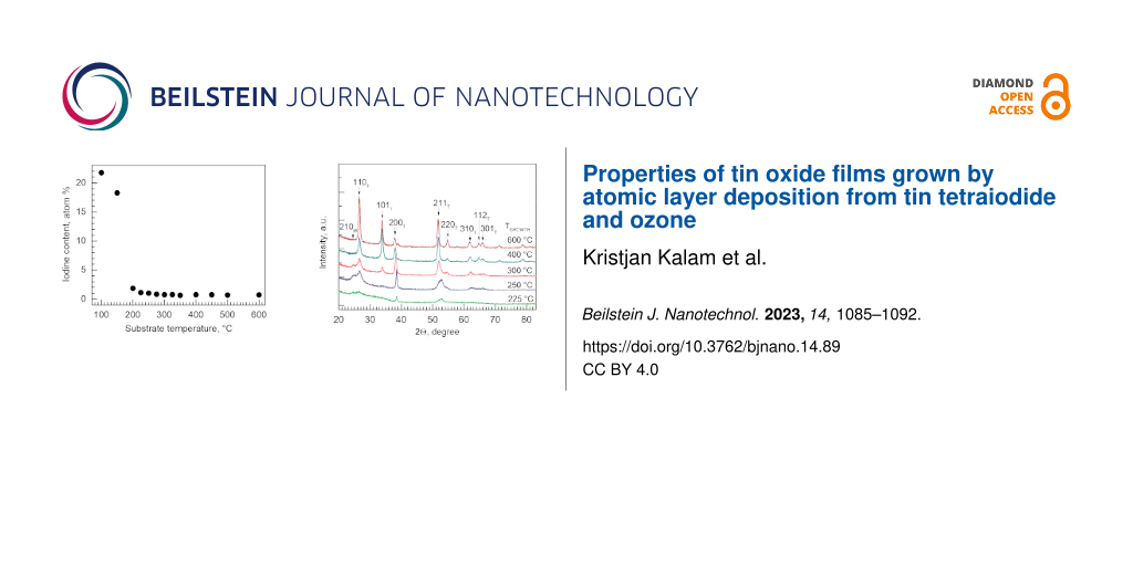
Analysis of oxygen and iodine contents in the films revealed that above a substrate temperature of 200 °C, the oxygen content remained stable. At temperatures below 200 °C, the oxygen content was significantly higher than that expected from a stoichiometric metal dioxide (Figure 6). A similar behaviour was observed for the iodine content. The films grown at temperatures below 200 °C were characterized by a markedly high iodine content (Figure 7). The iodine content decreased upon increasing the deposition temperature above 200 °C and, above 300 °C, stabilized at an appreciably low level of 0.7–0.8 atom % (Figure 7). Since the relatively high oxygen content below a deposition temperature of 200 °C did not arise from increased oxygen amounts in the film, but from decreased tin amounts, one can propose that, at the lowest deposition temperatures, I2O5 forms as a significant component in addition to the SnO2 host. Hence, a functional SnO2 film is most likely not realizable in this process below 200 °C. Even if formed, I2O5 would decompose at temperatures above 300 °C [22]. In our study, iodine and oxygen levels drop to the values low enough to obtain stoichiometric SnO2 as the major phase at temperatures higher than 300 °C.
![[2190-4286-14-89-6]](/bjnano/content/figures/2190-4286-14-89-6.png?scale=2.0&max-width=1024&background=FFFFFF)
Figure 6: Oxygen content in the SnO2 films as function of the substrate temperature.
Figure 6: Oxygen content in the SnO2 films as function of the substrate temperature.
![[2190-4286-14-89-7]](/bjnano/content/figures/2190-4286-14-89-7.png?scale=2.0&max-width=1024&background=FFFFFF)
Figure 7: Content of residual iodine in tin oxide films deposited from tin iodide and ozone in the temperature range of 100–600 °C.
Figure 7: Content of residual iodine in tin oxide films deposited from tin iodide and ozone in the temperatur...
Film structure
Increasing the deposition temperature increased the crystallinity of films, as can be seen in Figure 8. Diffractograms of all crystalline films revealed the presence of tetragonal SnO2 (PDF Card 01-071-5324). Depositions were carried out starting from 100 °C; however, XRD patterns from the films deposited at the lowest temperatures of 100–200 °C are not depicted in Figure 8 since the films grown at 225 °C were the first that revealed distinguishable reflections. The latter likely means that a significant portion of the films deposited below 200 °C is not SnO2. One diffraction maximum at 24.5° that exists in samples up to 300 °C is not attributable to any SnO2 phase. This is, however, the diffraction maximum of monoclinic I2O5 (PDF card 00-022-0338). This is consistent with the higher iodine and oxygen content measured in films deposited at lower temperatures.
![[2190-4286-14-89-8]](/bjnano/content/figures/2190-4286-14-89-8.png?scale=2.0&max-width=1024&background=FFFFFF)
Figure 8: GIXRD patterns of SnO2 films deposited at the given temperatures. Miller indices attributed to the diffraction maxima are indicated on the graph, where T corresponds to the tetragonal crystalline phase of SnO2 and M corresponds to the monoclinic phase of I2O5.
Figure 8: GIXRD patterns of SnO2 films deposited at the given temperatures. Miller indices attributed to the ...
The refractive indices of the films were stable throughout the sample series with different deposition temperatures, remaining between 2.04 and 2.06 at 633 nm wavelength for predominantly SnO2 films with little residuals. One representative dispersion curve from a film deposited at 300 °C is presented in Figure 9.
![[2190-4286-14-89-9]](/bjnano/content/figures/2190-4286-14-89-9.png?scale=2.0&max-width=1024&background=FFFFFF)
Figure 9: Refractive index of a SnO2 film deposited at 300 °C to a thickness of 110 nm as function of the wavelength.
Figure 9: Refractive index of a SnO2 film deposited at 300 °C to a thickness of 110 nm as function of the wav...
The refractive index values in the range of 2.04–2.06 can be regarded as appreciably high for SnO2 thin films. Refractive index values of approx. 2.0 were measured by ellipsometry for SnO2 films grown by ALD from bis(1-dimethylamino-2-methyl-2-propoxide)Sn as the Sn precursor and either H2O plasma or O2 plasma as the oxygen source [23]. Refractive index values between 2.0 and 2.1, comparable to those measured in the present study, have been obtained in a paper reporting the results of thermal ALD of SnO2 from tetrakis(dimethylamino)tin as the Sn precursor and ozone as the oxygen source [24]. The refractive index values obtained in the present study exceed those measured from SnO2 films deposited using spray pyrolysis [25] but remain inferior to those of post-growth-annealed SnO films grown via successive ionic layer adsorption and reaction [26].
The SnO2 films grown at 300 and 500 °C, that is, those with low residual iodine content, were analysed ex situ in terms of surface chemistry using soft X-ray spectroscopy methods. The Sn 3d XPS data (Figure 10a) show almost identical spectra for the samples deposited at 300 and 500 °C, and the narrow Sn 3d line profiles suggest the formation of a single-phase compound. The 2+ and 4+ charge states possible for Sn in its oxides have only a small (approx. 0.8 eV) difference in binding energy, which is less than the linewidth (FWHM ≈ 1.2 eV) of either compound [27,28]. Therefore, for mixed-phase compounds an asymmetric widening of the overall line profiles is observed rather than the appearance of additional resolved peaks [27,28]. The Sn 3d5/2 XPS binding energy of 486.9 eV in our data also aligns well with stoichiometric SnO2 as reported previously [27-34], indicating a single-phase Sn 4+ compound in our samples.
![[2190-4286-14-89-10]](/bjnano/content/figures/2190-4286-14-89-10.png?scale=2.0&max-width=1024&background=FFFFFF)
Figure 10: XPS results of (a) Sn 3d, (b) O 1s, and (c) valence-band region of the SnO2 films deposited at 300 and 500 °C.
Figure 10: XPS results of (a) Sn 3d, (b) O 1s, and (c) valence-band region of the SnO2 films deposited at 300 ...
In O 1s XPS (Figure 10b), the dominant peak at 530.7 eV also aligns well with values earlier reported for SnO2 [32-34]. A bit surprisingly, the spectra obtained from the sample grown at the higher deposition temperature revealed a somewhat more intense peak at the binding energy typical of surface OH (Figure 10b). This might be related to the chemisorption and decomposition of environmental humidity, enhanced on more crystallised film surfaces. Such a surface OH contribution has been described earlier [33,34].
Complementarily, the valence-band photoelectron spectra (Figure 10c) closely resemble those reported for SnO2 [28] with a dominant peak just below 5 eV and further distinct features at around 7.5 and 11 eV. This is in rather stark contrast to the SnO valence band, where mainly the occupied Sn 5s states give rise to a significant peak at ca. 2.5 eV binding energy, whereas the peak at 5 eV is not as dominant [28,29,35].
X-ray absorption spectra (Figure 11) were additionally recorded to possibly detect any differences between the samples. The Sn 3d XAS band is constituted by transitions from the 3d core orbital to the unoccupied p and f symmetry states, as defined by the dipole selection rules common for optical (first-order) transitions (Δl = ±1), whereas the O 1s XAS probes the oxygen p character states [36].
![[2190-4286-14-89-11]](/bjnano/content/figures/2190-4286-14-89-11.png?scale=2.0&max-width=1024&background=FFFFFF)
Figure 11: XAS results depicting O 1s (a) and Sn 3d (b) spectra of the SnO2 films deposited at 300 and 500 °C.
Figure 11: XAS results depicting O 1s (a) and Sn 3d (b) spectra of the SnO2 films deposited at 300 and 500 °C.
The lowest excitation energy peak (at 533.6 eV) in the SnO2 O 1s XAS (Figure 11a) has been assigned to unoccupied O 2p states hybridised with ligand Sn 5s states, while the three consecutive peaks at approximately 536.3, 537.7, and 539.6 eV correspond to states hybridised with Sn 5p states [37,38]. In the SnO2 rutile structure, the latter states are non-degenerate because of non-equidistant ligands for the axes of the coordination octahedron and the linking direction of these octahedra. We note that any eventual contribution from SnO (i.e., due to non-complete oxidation at lower deposition temperatures [39,40]) would show a quite different O 1s absorption spectrum with the lowest energy maximum downshifted by ca. 1 eV [28,29,35,36,41] and a broader and less intense feature in the region corresponding to the Sn 5p states, which then corresponds to an eg state split in C4v symmetry [37].
In the Sn 3d XAS results (Figure 11, right panel), the Sn 5s states are dipole-forbidden for transitions starting from the Sn 3d core level, whereas the triply split b1u, b2u and, b2u unoccupied states of Sn 5p origin in the D2h ligand symmetry, resulting in the three peaks at approximately 491, 493, and 495 eV (Figure 11b) in the Sn3d5/2 region, are characteristic of SnO2 [28,29,37,39,41]. The SnO Sn 3d spectrum is quite different with the Sn 3d5/2 main peak at almost 4 eV lower excitation energy (ca. 487 eV) [29,40,41] and no distinct triple peak structure, while the highest of the SnO2 triplet would already overlap with the SnO spin–orbit component (the Sn 3d3/2) main peak. In our opinion, the somewhat less sharp spectral shape and the slightly elevated relative intensity ratio of the 495 eV peak compared to the lower-energy 3d5/2 (491 and 493 eV) peaks suggests a minor SnO component present in the sample deposited at 300 °C. Alternatively, it is just a less structurally homogeneous sample, where slightly varying ligand distances average to less sharp XAS peaks.
Because of the somewhat less shallow probe depth of XAS recorded in TEY mode (ca. 10 nm) compared to the high surface sensitivity of the recorded photoemission spectra (a few atomic layers) [41] we suggest that less completely oxidised species appear below the outmost surface of the film.
Conclusion
SnO2 thin films were deposited from SnI4 and O3 via ALD in the temperature range of 100–600 °C. The resulting films formed in the crystalline tetragonal phase of SnO2 when the deposition temperature was over 225 °C, and the proportion of crystallised material in the film grew with the deposition temperature. Films grown at 200 °C and lower temperatures did not exhibit ordered structure and contained high amounts of residual iodine. Also, the oxygen fraction was larger than that expected from stoichiometric SnO2. Starting from about 300 °C, the precursor chemistry applied and reported in this work provides a fast route to SnO2 films with clearly defined structural properties. The growth per cycle of the films was about 0.25 nm/cycle. The deposition temperature can be lower than the minimally 400 °C needed for a process using SnI4 and O2, and the growth per cycle is about two times larger than for a process using SnI4 and O2.
Supporting Information
| Supporting Information File 1: Supplementary material. | ||
| Format: PDF | Size: 196.0 KB | Download |
Funding
The study was partially supported by the European Regional Development Fund projects Nos. TT20 and 2014-2020.4.01.20-0278 „Developing new research services and research infrastructures at MAX IV synchrotron radiation source“ (MAX-TEENUS), “Emerging orders in quantum and nanomaterials” (TK134), and the Estonian Research Agency (PRG753). We acknowledge MAX IV Laboratory for time on Beamline FinEstBeAMS under Proposal 20220073. Research conducted at MAX IV, a Swedish national user facility, is supported by the Swedish Research council under contract 2018-07152, the Swedish Governmental Agency for Innovation Systems under contract 2018-04969, and Formas under contract 2019-02496.
References
-
Aravindan, V.; Jinesh, K. B.; Prabhakar, R. R.; Kale, V. S.; Madhavi, S. Nano Energy 2013, 2, 720–725. doi:10.1016/j.nanoen.2012.12.007
Return to citation in text: [1] -
Choi, G.; Satyanarayana, L.; Park, J. Appl. Surf. Sci. 2006, 252, 7878–7883. doi:10.1016/j.apsusc.2005.09.069
Return to citation in text: [1] -
Barr, M. K. S.; Assaud, L.; Brazeau, N.; Hanbücken, M.; Ntais, S.; Santinacci, L.; Baranova, E. A. J. Phys. Chem. C 2017, 121, 17727–17736. doi:10.1021/acs.jpcc.7b05799
Return to citation in text: [1] -
Kavan, L.; Steier, L.; Grätzel, M. J. Phys. Chem. C 2017, 121, 342–350. doi:10.1021/acs.jpcc.6b09965
Return to citation in text: [1] -
Ren, N.; Zhu, C.; Li, R.; Mazumdar, S.; Sun, C.; Chen, B.; Xu, Q.; Wang, P.; Shi, B.; Huang, Q.; Xu, S.; Li, T.; Zhao, Y.; Zhang, X. Appl. Phys. Lett. 2022, 121, 033502. doi:10.1063/5.0091311
Return to citation in text: [1] -
Tamm, A.; Piirsoo, H.-M.; Jõgiaas, T.; Tarre, A.; Link, J.; Stern, R.; Kukli, K. Nanomaterials 2021, 11, 1633. doi:10.3390/nano11071633
Return to citation in text: [1] -
Hussain, S.; Erikson, H.; Kongi, N.; Rähn, M.; Merisalu, M.; Tamm, A.; Sammelselg, V.; Alonso-Vante, N.; Tammeveski, K. J. Electroanal. Chem. 2021, 896, 115147. doi:10.1016/j.jelechem.2021.115147
Return to citation in text: [1] -
Zhao, B.; Mattelaer, F.; Kint, J.; Werbrouck, A.; Henderick, L.; Minjauw, M.; Dendooven, J.; Detavernier, C. Electrochim. Acta 2019, 320, 134604. doi:10.1016/j.electacta.2019.134604
Return to citation in text: [1] -
Macco, B.; Kessels, W. M. M. Appl. Phys. Rev. 2022, 9, 041313. doi:10.1063/5.0116732
Return to citation in text: [1] -
Tarre, A.; Rosental, A.; Aidla, A.; Aarik, J.; Sundqvist, J.; Hårsta, A. Vacuum 2002, 67, 571–575. doi:10.1016/s0042-207x(02)00250-6
Return to citation in text: [1] [2] [3] [4] -
Rosental, A.; Tarre, A.; Gerst, A.; Sundqvist, J.; Hårsta, A.; Aidla, A.; Aarik, J.; Sammelselg, V.; Uustare, T. Sens. Actuators, B 2003, 93, 552–555. doi:10.1016/s0925-4005(03)00236-3
Return to citation in text: [1] [2] [3] -
Tarre, A.; Rosental, A.; Sundqvist, J.; Hårsta, A.; Uustare, T.; Sammelselg, V. Surf. Sci. 2003, 532–535, 514–518. doi:10.1016/s0039-6028(03)00476-x
Return to citation in text: [1] [2] -
Sundqvist, J.; Tarre, A.; Rosental, A.; Hårsta, A. Chem. Vap. Deposition 2003, 9, 21–25. doi:10.1002/cvde.200290002
Return to citation in text: [1] [2] [3] -
Sundqvist, J.; Lu, J.; Ottosson, M.; Hårsta, A. Thin Solid Films 2006, 514, 63–68. doi:10.1016/j.tsf.2006.02.031
Return to citation in text: [1] [2] [3] -
Lu, J.; Sundqvist, J.; Ottosson, M.; Tarre, A.; Rosental, A.; Aarik, J.; Hårsta, A. J. Cryst. Growth 2004, 260, 191–200. doi:10.1016/j.jcrysgro.2003.08.042
Return to citation in text: [1] -
Arroval, T.; Aarik, L.; Rammula, R.; Kruusla, V.; Aarik, J. Thin Solid Films 2016, 600, 119–125. doi:10.1016/j.tsf.2016.01.024
Return to citation in text: [1] -
Aarik, L.; Alles, H.; Aidla, A.; Kahro, T.; Kukli, K.; Niinistö, J.; Mändar, H.; Tamm, A.; Rammula, R.; Sammelselg, V.; Aarik, J. Thin Solid Films 2014, 565, 37–44. doi:10.1016/j.tsf.2014.06.052
Return to citation in text: [1] -
Chernenko, K.; Kivimäki, A.; Pärna, R.; Wang, W.; Sankari, R.; Leandersson, M.; Tarawneh, H.; Pankratov, V.; Kook, M.; Kukk, E.; Reisberg, L.; Urpelainen, S.; Käämbre, T.; Siewert, F.; Gwalt, G.; Sokolov, A.; Lemke, S.; Alimov, S.; Knedel, J.; Kutz, O.; Seliger, T.; Valden, M.; Hirsimäki, M.; Kirm, M.; Huttula, M. J. Synchrotron Radiat. 2021, 28, 1620–1630. doi:10.1107/s1600577521006032
Return to citation in text: [1] -
Wang, W.; Kivimäki, A.; Chernenko, K.; Pärna, R.; Käämbre, T.; Kukk, E.; Kokko, K.; Valden, M.; Hirsimäki, M.; Kirm, M.; Huttula, M. J. Phys.: Conf. Ser. 2022, 2380, 012048. doi:10.1088/1742-6596/2380/1/012048
Return to citation in text: [1] -
Suntola, T. Appl. Surf. Sci. 1996, 100–101, 391–398. doi:10.1016/0169-4332(96)00306-6
Return to citation in text: [1] -
Schuisky, M.; Aarik, J.; Kukli, K.; Aidla, A.; Hårsta, A. Langmuir 2001, 17, 5508–5512. doi:10.1021/la010174+
Return to citation in text: [1] [2] -
Hobosyan, M. A.; Martirosyan, K. S. Propellants, Explos., Pyrotech. 2017, 42, 506–513. doi:10.1002/prep.201600220
Return to citation in text: [1] -
Won, J. H.; Han, S. H.; Park, B. K.; Chung, T.-M.; Han, J. H. Coatings 2020, 10, 692. doi:10.3390/coatings10070692
Return to citation in text: [1] -
Choi, D.-W.; Park, J.-S. Surf. Coat. Technol. 2014, 259, 238–243. doi:10.1016/j.surfcoat.2014.02.012
Return to citation in text: [1] -
Erken, O.; Ozkendir, O. M.; Gunes, M.; Harputlu, E.; Ulutas, C.; Gumus, C. Ceram. Int. 2019, 45, 19086–19092. doi:10.1016/j.ceramint.2019.06.153
Return to citation in text: [1] -
Yıldırım, M. A.; Yıldırım, S. T.; Sakar, E. F.; Ateş, A. Spectrochim. Acta, Part A 2014, 133, 60–65. doi:10.1016/j.saa.2014.05.035
Return to citation in text: [1] -
Fondell, M.; Gorgoi, M.; Boman, M.; Lindblad, A. J. Electron Spectrosc. Relat. Phenom. 2014, 195, 195–199. doi:10.1016/j.elspec.2014.07.012
Return to citation in text: [1] [2] [3] -
Minohara, M.; Kikuchi, N.; Yoshida, Y.; Kumigashira, H.; Aiura, Y. J. Mater. Chem. C 2019, 7, 6332–6336. doi:10.1039/c9tc01297d
Return to citation in text: [1] [2] [3] [4] [5] [6] [7] -
Bouras, K.; Schmerber, G.; Aureau, D.; Rinnert, H.; Ferblantier, G.; Fix, T.; Colis, S.; Bazylewski, P.; Leedahl, B.; Etcheberry, A.; Chang, G. S.; Dinia, A.; Slaoui, A. RSC Adv. 2016, 6, 67157–67165. doi:10.1039/c6ra14460h
Return to citation in text: [1] [2] [3] [4] [5] -
Ahn, H.-J.; Choi, H.-C.; Park, K.-W.; Kim, S.-B.; Sung, Y.-E. J. Phys. Chem. B 2004, 108, 9815–9820. doi:10.1021/jp035769n
Return to citation in text: [1] -
Xia, W.; Wang, H.; Zeng, X.; Han, J.; Zhu, J.; Zhou, M.; Wu, S. CrystEngComm 2014, 16, 6841–6847. doi:10.1039/c4ce00884g
Return to citation in text: [1] -
Won, J. H.; Choi, H.; Han, S. H.; Park, B. K.; Chung, T.-M.; Han, J. H. Vacuum 2022, 196, 110739. doi:10.1016/j.vacuum.2021.110739
Return to citation in text: [1] [2] -
Pan, X. Q.; Fu, L. J. Appl. Phys. 2001, 89, 6048–6055. doi:10.1063/1.1368865
Return to citation in text: [1] [2] [3] -
Gubbala, S.; Russell, H. B.; Shah, H.; Deb, B.; Jasinski, J.; Rypkema, H.; Sunkara, M. K. Energy Environ. Sci. 2009, 2, 1302–1309. doi:10.1039/b910174h
Return to citation in text: [1] [2] [3] -
McLeod, J. A.; Skorikov, N. A.; Finkelstein, L. D.; Kurmaev, E. Z.; Moewes, A. J. Phys. Chem. C 2012, 116, 24248–24254. doi:10.1021/jp3077134
Return to citation in text: [1] [2] -
Frati, F.; Hunault, M. O. J. Y.; de Groot, F. M. F. Chem. Rev. 2020, 120, 4056–4110. doi:10.1021/acs.chemrev.9b00439
Return to citation in text: [1] [2] -
Chouvin, J.; Olivier-Fourcade, J.; Jumas, J. C.; Simon, B.; Biensan, P.; Fernández Madrigal, F. J.; Tirado, J. L.; Pérez Vicente, C. J. Electroanal. Chem. 2000, 494, 136–146. doi:10.1016/s0022-0728(00)00357-0
Return to citation in text: [1] [2] [3] -
Kurganskii, S. I.; Manyakin, M. D.; Dubrovskii, O. I.; Chuvenkova, O. A.; Turishchev, S. Y.; Domashevskaya, E. P. Phys. Solid State 2014, 56, 1748–1753. doi:10.1134/s1063783414090170
Return to citation in text: [1] -
Gago, R.; Prucnal, S.; Azpeitia, J.; Esteban-Mendoza, D.; Jiménez, I. J. Alloys Compd. 2022, 902, 163768. doi:10.1016/j.jallcom.2022.163768
Return to citation in text: [1] [2] -
Braglia, L.; Fracchia, M.; Ghigna, P.; Minguzzi, A.; Meroni, D.; Edla, R.; Vandichel, M.; Ahlberg, E.; Cerrato, G.; Torelli, P. J. Phys. Chem. C 2020, 124, 14202–14212. doi:10.1021/acs.jpcc.0c02546
Return to citation in text: [1] [2] -
Tanuma, S.; Powell, C. J.; Penn, D. R. Surf. Interface Anal. 2005, 37, 1–14. doi:10.1002/sia.1997
Return to citation in text: [1] [2] [3] [4]
| 27. | Fondell, M.; Gorgoi, M.; Boman, M.; Lindblad, A. J. Electron Spectrosc. Relat. Phenom. 2014, 195, 195–199. doi:10.1016/j.elspec.2014.07.012 |
| 28. | Minohara, M.; Kikuchi, N.; Yoshida, Y.; Kumigashira, H.; Aiura, Y. J. Mater. Chem. C 2019, 7, 6332–6336. doi:10.1039/c9tc01297d |
| 27. | Fondell, M.; Gorgoi, M.; Boman, M.; Lindblad, A. J. Electron Spectrosc. Relat. Phenom. 2014, 195, 195–199. doi:10.1016/j.elspec.2014.07.012 |
| 28. | Minohara, M.; Kikuchi, N.; Yoshida, Y.; Kumigashira, H.; Aiura, Y. J. Mater. Chem. C 2019, 7, 6332–6336. doi:10.1039/c9tc01297d |
| 29. | Bouras, K.; Schmerber, G.; Aureau, D.; Rinnert, H.; Ferblantier, G.; Fix, T.; Colis, S.; Bazylewski, P.; Leedahl, B.; Etcheberry, A.; Chang, G. S.; Dinia, A.; Slaoui, A. RSC Adv. 2016, 6, 67157–67165. doi:10.1039/c6ra14460h |
| 30. | Ahn, H.-J.; Choi, H.-C.; Park, K.-W.; Kim, S.-B.; Sung, Y.-E. J. Phys. Chem. B 2004, 108, 9815–9820. doi:10.1021/jp035769n |
| 31. | Xia, W.; Wang, H.; Zeng, X.; Han, J.; Zhu, J.; Zhou, M.; Wu, S. CrystEngComm 2014, 16, 6841–6847. doi:10.1039/c4ce00884g |
| 32. | Won, J. H.; Choi, H.; Han, S. H.; Park, B. K.; Chung, T.-M.; Han, J. H. Vacuum 2022, 196, 110739. doi:10.1016/j.vacuum.2021.110739 |
| 33. | Pan, X. Q.; Fu, L. J. Appl. Phys. 2001, 89, 6048–6055. doi:10.1063/1.1368865 |
| 34. | Gubbala, S.; Russell, H. B.; Shah, H.; Deb, B.; Jasinski, J.; Rypkema, H.; Sunkara, M. K. Energy Environ. Sci. 2009, 2, 1302–1309. doi:10.1039/b910174h |
| 1. | Aravindan, V.; Jinesh, K. B.; Prabhakar, R. R.; Kale, V. S.; Madhavi, S. Nano Energy 2013, 2, 720–725. doi:10.1016/j.nanoen.2012.12.007 |
| 5. | Ren, N.; Zhu, C.; Li, R.; Mazumdar, S.; Sun, C.; Chen, B.; Xu, Q.; Wang, P.; Shi, B.; Huang, Q.; Xu, S.; Li, T.; Zhao, Y.; Zhang, X. Appl. Phys. Lett. 2022, 121, 033502. doi:10.1063/5.0091311 |
| 16. | Arroval, T.; Aarik, L.; Rammula, R.; Kruusla, V.; Aarik, J. Thin Solid Films 2016, 600, 119–125. doi:10.1016/j.tsf.2016.01.024 |
| 28. | Minohara, M.; Kikuchi, N.; Yoshida, Y.; Kumigashira, H.; Aiura, Y. J. Mater. Chem. C 2019, 7, 6332–6336. doi:10.1039/c9tc01297d |
| 29. | Bouras, K.; Schmerber, G.; Aureau, D.; Rinnert, H.; Ferblantier, G.; Fix, T.; Colis, S.; Bazylewski, P.; Leedahl, B.; Etcheberry, A.; Chang, G. S.; Dinia, A.; Slaoui, A. RSC Adv. 2016, 6, 67157–67165. doi:10.1039/c6ra14460h |
| 35. | McLeod, J. A.; Skorikov, N. A.; Finkelstein, L. D.; Kurmaev, E. Z.; Moewes, A. J. Phys. Chem. C 2012, 116, 24248–24254. doi:10.1021/jp3077134 |
| 36. | Frati, F.; Hunault, M. O. J. Y.; de Groot, F. M. F. Chem. Rev. 2020, 120, 4056–4110. doi:10.1021/acs.chemrev.9b00439 |
| 41. | Tanuma, S.; Powell, C. J.; Penn, D. R. Surf. Interface Anal. 2005, 37, 1–14. doi:10.1002/sia.1997 |
| 4. | Kavan, L.; Steier, L.; Grätzel, M. J. Phys. Chem. C 2017, 121, 342–350. doi:10.1021/acs.jpcc.6b09965 |
| 17. | Aarik, L.; Alles, H.; Aidla, A.; Kahro, T.; Kukli, K.; Niinistö, J.; Mändar, H.; Tamm, A.; Rammula, R.; Sammelselg, V.; Aarik, J. Thin Solid Films 2014, 565, 37–44. doi:10.1016/j.tsf.2014.06.052 |
| 37. | Chouvin, J.; Olivier-Fourcade, J.; Jumas, J. C.; Simon, B.; Biensan, P.; Fernández Madrigal, F. J.; Tirado, J. L.; Pérez Vicente, C. J. Electroanal. Chem. 2000, 494, 136–146. doi:10.1016/s0022-0728(00)00357-0 |
| 3. | Barr, M. K. S.; Assaud, L.; Brazeau, N.; Hanbücken, M.; Ntais, S.; Santinacci, L.; Baranova, E. A. J. Phys. Chem. C 2017, 121, 17727–17736. doi:10.1021/acs.jpcc.7b05799 |
| 10. | Tarre, A.; Rosental, A.; Aidla, A.; Aarik, J.; Sundqvist, J.; Hårsta, A. Vacuum 2002, 67, 571–575. doi:10.1016/s0042-207x(02)00250-6 |
| 11. | Rosental, A.; Tarre, A.; Gerst, A.; Sundqvist, J.; Hårsta, A.; Aidla, A.; Aarik, J.; Sammelselg, V.; Uustare, T. Sens. Actuators, B 2003, 93, 552–555. doi:10.1016/s0925-4005(03)00236-3 |
| 12. | Tarre, A.; Rosental, A.; Sundqvist, J.; Hårsta, A.; Uustare, T.; Sammelselg, V. Surf. Sci. 2003, 532–535, 514–518. doi:10.1016/s0039-6028(03)00476-x |
| 13. | Sundqvist, J.; Tarre, A.; Rosental, A.; Hårsta, A. Chem. Vap. Deposition 2003, 9, 21–25. doi:10.1002/cvde.200290002 |
| 14. | Sundqvist, J.; Lu, J.; Ottosson, M.; Hårsta, A. Thin Solid Films 2006, 514, 63–68. doi:10.1016/j.tsf.2006.02.031 |
| 37. | Chouvin, J.; Olivier-Fourcade, J.; Jumas, J. C.; Simon, B.; Biensan, P.; Fernández Madrigal, F. J.; Tirado, J. L.; Pérez Vicente, C. J. Electroanal. Chem. 2000, 494, 136–146. doi:10.1016/s0022-0728(00)00357-0 |
| 38. | Kurganskii, S. I.; Manyakin, M. D.; Dubrovskii, O. I.; Chuvenkova, O. A.; Turishchev, S. Y.; Domashevskaya, E. P. Phys. Solid State 2014, 56, 1748–1753. doi:10.1134/s1063783414090170 |
| 2. | Choi, G.; Satyanarayana, L.; Park, J. Appl. Surf. Sci. 2006, 252, 7878–7883. doi:10.1016/j.apsusc.2005.09.069 |
| 13. | Sundqvist, J.; Tarre, A.; Rosental, A.; Hårsta, A. Chem. Vap. Deposition 2003, 9, 21–25. doi:10.1002/cvde.200290002 |
| 14. | Sundqvist, J.; Lu, J.; Ottosson, M.; Hårsta, A. Thin Solid Films 2006, 514, 63–68. doi:10.1016/j.tsf.2006.02.031 |
| 39. | Gago, R.; Prucnal, S.; Azpeitia, J.; Esteban-Mendoza, D.; Jiménez, I. J. Alloys Compd. 2022, 902, 163768. doi:10.1016/j.jallcom.2022.163768 |
| 40. | Braglia, L.; Fracchia, M.; Ghigna, P.; Minguzzi, A.; Meroni, D.; Edla, R.; Vandichel, M.; Ahlberg, E.; Cerrato, G.; Torelli, P. J. Phys. Chem. C 2020, 124, 14202–14212. doi:10.1021/acs.jpcc.0c02546 |
| 9. | Macco, B.; Kessels, W. M. M. Appl. Phys. Rev. 2022, 9, 041313. doi:10.1063/5.0116732 |
| 10. | Tarre, A.; Rosental, A.; Aidla, A.; Aarik, J.; Sundqvist, J.; Hårsta, A. Vacuum 2002, 67, 571–575. doi:10.1016/s0042-207x(02)00250-6 |
| 11. | Rosental, A.; Tarre, A.; Gerst, A.; Sundqvist, J.; Hårsta, A.; Aidla, A.; Aarik, J.; Sammelselg, V.; Uustare, T. Sens. Actuators, B 2003, 93, 552–555. doi:10.1016/s0925-4005(03)00236-3 |
| 15. | Lu, J.; Sundqvist, J.; Ottosson, M.; Tarre, A.; Rosental, A.; Aarik, J.; Hårsta, A. J. Cryst. Growth 2004, 260, 191–200. doi:10.1016/j.jcrysgro.2003.08.042 |
| 28. | Minohara, M.; Kikuchi, N.; Yoshida, Y.; Kumigashira, H.; Aiura, Y. J. Mater. Chem. C 2019, 7, 6332–6336. doi:10.1039/c9tc01297d |
| 29. | Bouras, K.; Schmerber, G.; Aureau, D.; Rinnert, H.; Ferblantier, G.; Fix, T.; Colis, S.; Bazylewski, P.; Leedahl, B.; Etcheberry, A.; Chang, G. S.; Dinia, A.; Slaoui, A. RSC Adv. 2016, 6, 67157–67165. doi:10.1039/c6ra14460h |
| 35. | McLeod, J. A.; Skorikov, N. A.; Finkelstein, L. D.; Kurmaev, E. Z.; Moewes, A. J. Phys. Chem. C 2012, 116, 24248–24254. doi:10.1021/jp3077134 |
| 8. | Zhao, B.; Mattelaer, F.; Kint, J.; Werbrouck, A.; Henderick, L.; Minjauw, M.; Dendooven, J.; Detavernier, C. Electrochim. Acta 2019, 320, 134604. doi:10.1016/j.electacta.2019.134604 |
| 10. | Tarre, A.; Rosental, A.; Aidla, A.; Aarik, J.; Sundqvist, J.; Hårsta, A. Vacuum 2002, 67, 571–575. doi:10.1016/s0042-207x(02)00250-6 |
| 36. | Frati, F.; Hunault, M. O. J. Y.; de Groot, F. M. F. Chem. Rev. 2020, 120, 4056–4110. doi:10.1021/acs.chemrev.9b00439 |
| 7. | Hussain, S.; Erikson, H.; Kongi, N.; Rähn, M.; Merisalu, M.; Tamm, A.; Sammelselg, V.; Alonso-Vante, N.; Tammeveski, K. J. Electroanal. Chem. 2021, 896, 115147. doi:10.1016/j.jelechem.2021.115147 |
| 33. | Pan, X. Q.; Fu, L. J. Appl. Phys. 2001, 89, 6048–6055. doi:10.1063/1.1368865 |
| 34. | Gubbala, S.; Russell, H. B.; Shah, H.; Deb, B.; Jasinski, J.; Rypkema, H.; Sunkara, M. K. Energy Environ. Sci. 2009, 2, 1302–1309. doi:10.1039/b910174h |
| 6. | Tamm, A.; Piirsoo, H.-M.; Jõgiaas, T.; Tarre, A.; Link, J.; Stern, R.; Kukli, K. Nanomaterials 2021, 11, 1633. doi:10.3390/nano11071633 |
| 10. | Tarre, A.; Rosental, A.; Aidla, A.; Aarik, J.; Sundqvist, J.; Hårsta, A. Vacuum 2002, 67, 571–575. doi:10.1016/s0042-207x(02)00250-6 |
| 11. | Rosental, A.; Tarre, A.; Gerst, A.; Sundqvist, J.; Hårsta, A.; Aidla, A.; Aarik, J.; Sammelselg, V.; Uustare, T. Sens. Actuators, B 2003, 93, 552–555. doi:10.1016/s0925-4005(03)00236-3 |
| 12. | Tarre, A.; Rosental, A.; Sundqvist, J.; Hårsta, A.; Uustare, T.; Sammelselg, V. Surf. Sci. 2003, 532–535, 514–518. doi:10.1016/s0039-6028(03)00476-x |
| 13. | Sundqvist, J.; Tarre, A.; Rosental, A.; Hårsta, A. Chem. Vap. Deposition 2003, 9, 21–25. doi:10.1002/cvde.200290002 |
| 14. | Sundqvist, J.; Lu, J.; Ottosson, M.; Hårsta, A. Thin Solid Films 2006, 514, 63–68. doi:10.1016/j.tsf.2006.02.031 |
| 28. | Minohara, M.; Kikuchi, N.; Yoshida, Y.; Kumigashira, H.; Aiura, Y. J. Mater. Chem. C 2019, 7, 6332–6336. doi:10.1039/c9tc01297d |
| 20. | Suntola, T. Appl. Surf. Sci. 1996, 100–101, 391–398. doi:10.1016/0169-4332(96)00306-6 |
| 18. | Chernenko, K.; Kivimäki, A.; Pärna, R.; Wang, W.; Sankari, R.; Leandersson, M.; Tarawneh, H.; Pankratov, V.; Kook, M.; Kukk, E.; Reisberg, L.; Urpelainen, S.; Käämbre, T.; Siewert, F.; Gwalt, G.; Sokolov, A.; Lemke, S.; Alimov, S.; Knedel, J.; Kutz, O.; Seliger, T.; Valden, M.; Hirsimäki, M.; Kirm, M.; Huttula, M. J. Synchrotron Radiat. 2021, 28, 1620–1630. doi:10.1107/s1600577521006032 |
| 28. | Minohara, M.; Kikuchi, N.; Yoshida, Y.; Kumigashira, H.; Aiura, Y. J. Mater. Chem. C 2019, 7, 6332–6336. doi:10.1039/c9tc01297d |
| 29. | Bouras, K.; Schmerber, G.; Aureau, D.; Rinnert, H.; Ferblantier, G.; Fix, T.; Colis, S.; Bazylewski, P.; Leedahl, B.; Etcheberry, A.; Chang, G. S.; Dinia, A.; Slaoui, A. RSC Adv. 2016, 6, 67157–67165. doi:10.1039/c6ra14460h |
| 37. | Chouvin, J.; Olivier-Fourcade, J.; Jumas, J. C.; Simon, B.; Biensan, P.; Fernández Madrigal, F. J.; Tirado, J. L.; Pérez Vicente, C. J. Electroanal. Chem. 2000, 494, 136–146. doi:10.1016/s0022-0728(00)00357-0 |
| 39. | Gago, R.; Prucnal, S.; Azpeitia, J.; Esteban-Mendoza, D.; Jiménez, I. J. Alloys Compd. 2022, 902, 163768. doi:10.1016/j.jallcom.2022.163768 |
| 41. | Tanuma, S.; Powell, C. J.; Penn, D. R. Surf. Interface Anal. 2005, 37, 1–14. doi:10.1002/sia.1997 |
| 19. | Wang, W.; Kivimäki, A.; Chernenko, K.; Pärna, R.; Käämbre, T.; Kukk, E.; Kokko, K.; Valden, M.; Hirsimäki, M.; Kirm, M.; Huttula, M. J. Phys.: Conf. Ser. 2022, 2380, 012048. doi:10.1088/1742-6596/2380/1/012048 |
| 29. | Bouras, K.; Schmerber, G.; Aureau, D.; Rinnert, H.; Ferblantier, G.; Fix, T.; Colis, S.; Bazylewski, P.; Leedahl, B.; Etcheberry, A.; Chang, G. S.; Dinia, A.; Slaoui, A. RSC Adv. 2016, 6, 67157–67165. doi:10.1039/c6ra14460h |
| 40. | Braglia, L.; Fracchia, M.; Ghigna, P.; Minguzzi, A.; Meroni, D.; Edla, R.; Vandichel, M.; Ahlberg, E.; Cerrato, G.; Torelli, P. J. Phys. Chem. C 2020, 124, 14202–14212. doi:10.1021/acs.jpcc.0c02546 |
| 41. | Tanuma, S.; Powell, C. J.; Penn, D. R. Surf. Interface Anal. 2005, 37, 1–14. doi:10.1002/sia.1997 |
| 41. | Tanuma, S.; Powell, C. J.; Penn, D. R. Surf. Interface Anal. 2005, 37, 1–14. doi:10.1002/sia.1997 |
| 26. | Yıldırım, M. A.; Yıldırım, S. T.; Sakar, E. F.; Ateş, A. Spectrochim. Acta, Part A 2014, 133, 60–65. doi:10.1016/j.saa.2014.05.035 |
| 27. | Fondell, M.; Gorgoi, M.; Boman, M.; Lindblad, A. J. Electron Spectrosc. Relat. Phenom. 2014, 195, 195–199. doi:10.1016/j.elspec.2014.07.012 |
| 28. | Minohara, M.; Kikuchi, N.; Yoshida, Y.; Kumigashira, H.; Aiura, Y. J. Mater. Chem. C 2019, 7, 6332–6336. doi:10.1039/c9tc01297d |
| 24. | Choi, D.-W.; Park, J.-S. Surf. Coat. Technol. 2014, 259, 238–243. doi:10.1016/j.surfcoat.2014.02.012 |
| 25. | Erken, O.; Ozkendir, O. M.; Gunes, M.; Harputlu, E.; Ulutas, C.; Gumus, C. Ceram. Int. 2019, 45, 19086–19092. doi:10.1016/j.ceramint.2019.06.153 |
| 22. | Hobosyan, M. A.; Martirosyan, K. S. Propellants, Explos., Pyrotech. 2017, 42, 506–513. doi:10.1002/prep.201600220 |
| 23. | Won, J. H.; Han, S. H.; Park, B. K.; Chung, T.-M.; Han, J. H. Coatings 2020, 10, 692. doi:10.3390/coatings10070692 |
| 21. | Schuisky, M.; Aarik, J.; Kukli, K.; Aidla, A.; Hårsta, A. Langmuir 2001, 17, 5508–5512. doi:10.1021/la010174+ |
| 21. | Schuisky, M.; Aarik, J.; Kukli, K.; Aidla, A.; Hårsta, A. Langmuir 2001, 17, 5508–5512. doi:10.1021/la010174+ |
© 2023 Kalam et al.; licensee Beilstein-Institut.
This is an open access article licensed under the terms of the Beilstein-Institut Open Access License Agreement (https://www.beilstein-journals.org/bjnano/terms), which is identical to the Creative Commons Attribution 4.0 International License (https://creativecommons.org/licenses/by/4.0). The reuse of material under this license requires that the author(s), source and license are credited. Third-party material in this article could be subject to other licenses (typically indicated in the credit line), and in this case, users are required to obtain permission from the license holder to reuse the material.