1SUNAG Laboratory, Institute of Physics, Bhubaneswar 751 005, Odisha, India
2Homi Bhabha National Institute, Training School Complex, Anushakti Nagar, Mumbai 400 094, India
3Department of Physics, Alagappa University, Karaikudi 630 003, India
4Department of Physics, Indian Institute of Technology Kharagpur, Kharagpur 721 302, India
Corresponding author email
‡ Equal contributors
Associate Editor: L. Fu Beilstein J. Nanotechnol.2024,15, 350–359.https://doi.org/10.3762/bjnano.15.31 Received 08 Nov 2023,
Accepted 13 Mar 2024,
Published 02 Apr 2024
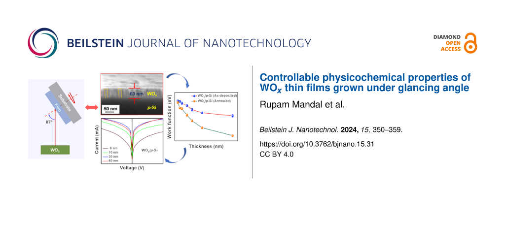
In this work, various physicochemical properties are investigated in nanostructured WOx thin films prepared by radio-frequency magnetron sputtering for optoelectronic applications. A glancing angle of 87° is employed to grow films of different thicknesses, which are then exposed to post-growth annealing. Detailed local probe analyses in terms of morphology and work function of WOx films are carried out to investigate thickness-dependent property modulations of the as-deposited and annealed films. The analyses show a reasonably good correlation with photoelectron spectroscopic measurements on the films and the bulk I–V characteristics acquired on a series of WOx/p-Si heterojunction diodes. The presence of a critical WOx thickness is identified to regulate the rectification ratio values at the WOx/p-Si heterostructures and increase in series resistance within the bulk of the films. The present study provides valuable insights to correlate optical, electrical, and structural properties of WOx thin films, which will be beneficial for fabricating WOx-based optoelectronic devices, including photovoltaic cells.
Tungsten oxide (WOx; x ≤ 3) is a popular transition-metal oxide for various optoelectronic devices because of its fascinating optical and electrical properties [1]. WOx is a wide-bandgap oxide semiconductor with a large excitonic binding energy of 0.15 eV and a high optical absorption coefficient (≥104 cm−1 in the UV region) [2]. These, in conjunction with decent carrier mobility (12 cm2·V−1·s−1), make this material an ideal candidate for UV photodetector applications [3]. Because of its octahedral lattice symmetry and partially filled d bands, WOx is also highly attractive as an electrochromic material for developing modern-day smart windows and display devices [4-7]. Exhibiting various stoichiometric and sub-stoichiometric compositions and polymorphs, WOx usually behaves as an n-type semiconductor because an unintentional incorporation of a certain amount of reduced W cations is thermodynamically inevitable in these films [8]. It is, therefore, possible to tune the physicochemical properties, such as work function, bandgap, and electrical conductivity, to a large extent by controlling the cationic oxidation state and the film stoichiometry [2]. As a matter of fact, adjustments in the film stoichiometry and microstructure are experimentally viable by the choice of a suitable growth technique [9-11]. As a result, heterostructures having an n-type WOx layer on various p-type substrates such as p-Si [12,13], Cu2O [14], NiO [15], p-ZnO nanowires (NWs) [16], diamond [17], and BiVO4[18], have a great technological importance in the field of heterojunction solar cells, LEDs, and resistance random access memory (RRAM) devices. In this regard, radio frequency (rf) sputter deposition is one of the preferred choices as an industry-compatible method to grow WOx thin films [2,19-21].
Apart from thin films, nanostructured metal oxides generally possess superior electrochemical properties compared to their bulk counterparts [2]. WOx nanostructures, exhibiting high chemical and thermal stability, and structural flexibility, have obvious relevance in areas such as photocatalysis [22], electrochromism [23], supercapacitors [24], and lithium batteries [25] and have undergone extensive investigations during the last decades. In this respect, the use of glancing angle deposition (GLAD) to produce high-aspect-ratio nanostructures has certain advantages in terms of a wide range of structural possibilities (such as screws and helical or columnar structures) and reduced complexity (no templates involved) [26]. In addition, film crystallinity and compositional variations in such films can also be adjusted as a function of the growth angle [27,28], making GLAD a promising approach to yield nanostructured (NS) films [29-31]. Electronic devices consisting of multilayers often require information on surface electrochemical property variation of the underlying films induced by structural changes. Therefore, a systematic investigation on the surface work function of the NS-WOx films as a function of thickness holds the potential for accessing its practical device application.
In this article, we report on tunable structural, optical, and electrical properties of glancing angle-deposited NS-WOx thin films, where NS-WOx films of different thicknesses (6–60 nm) are prepared by rf sputtering and exposed to post-growth annealing at 673 K in vacuum (2 × 10⁻⁷ mbar). The role of increased oxygen vacancy concentration (OV) on optical bandgap and work function is thoroughly investigated by employing various spectroscopic and microscopic techniques. The systematic investigation of the work function of the films reveals a distinct trend with thickness, originating from the thickness-dependent defect concentration within the films. It is observed that the as-deposited NS-WOx/p-Si heterostructures are quasi-ohmic in nature. The annealed counterparts exhibit a relatively higher rectification, which points towards a possible defect-dependent Fermi level pinning at the hetero-interface. Overall, our systematic experimental observations demonstrate a wide range of tunability and correlation among several physicochemical properties of glancing angle-deposited WOx films, which is due to serve as a guide for fabricating WOx-based optoelectronic devices, including carrier-selective contacts for photovoltaic cells.
Experimental
NS-WOx thin films were deposited on ultrasonically cleaned p-Si (100) and soda lime glass substrates of 1 × 1 cm2 dimension using a rf magnetron sputtering setup (Excel Instruments). Trichloroethylene, propanol, acetone, and DI water were used to carry out ultrasonication of the substrates for removing organic contaminants. Prior to the deposition, the substrates were properly air-dried. A 99.99% pure WO3 target (5 mm thick) was used to grow the WOx films. The initial pressure in the deposition chamber was 5 × 10⁻⁷ mbar, and the WOx films were deposited at 5 × 10⁻³ mbar working pressure by injecting ultrapure Ar gas (99.99%) using a mass flow controller at 30 sccm flow rate. The substrate holder was kept 12.5 cm away from the target at a glancing angle of 87° and 50 W rf power (Advanced Energy) was applied to the target, keeping the substrate holder grounded. Pre-sputtering was carried out for a duration of 1200 s to achieve stability in depositions and contamination-free films. A constant substrate rotation (10 rpm) was maintained to achieve uniform WOx films. Post-growth annealing of all WOx films (grown under the same conditions) was performed at 673 K for 60 min in a vacuum environment (3 × 10⁻⁷ mbar).
The thickness of the films was measured using a surface profilometer (Ambios, XP 200). The surface morphology of the as-deposited and the annealed films was acquired using tapping mode AFM (Asylum Research). AFM images were recorded at different places on each sample to confirm the film uniformity. WSxM software was used to carry out AFM image analysis.
Kelvin probe force microscopy (KPFM) was used to study the local work function of the WOx films. WOx samples were removed from the high-vacuum environment right before the KPFM measurements to avoid any contamination in air. For KPFM measurements, a conductive tip (Ti/Pt coated) having a resonance frequency of approx. 70 kHz, a stiffness of approx. 2 N·m−1, and a radius of curvature of approx. 30 nm was used for KPFM measurements. To examine the uniformity in work function values of each film, different regions on the sample surface were mapped. Also, variable scan angles and scan speeds (0.2 to 1 Hz) were used to avoid the undesired presence of artefacts in the measured data. A dry nitrogen atmosphere ensured a low humidity level of 8–10% during all the KPFM measurements [29]. Further, the I–V measurements on the WOx/p-Si heterostructures were performed by preparing Ag electrodes (1 mm diameter) on top of the WOx films and p-Si substrates. The I–V data were acquired by applying DC voltage sweeps (−1 V→0 V→+1 V) using a Keithley source meter (Model 2400, Tektronix, USA) in a sandwiched configuration. During the measurements, the bias voltage was applied to the p-Si substrates, whereas the WOx films were kept grounded.
The crystallinity of the WOx films was examined using X-ray diffraction (XRD) (Bruker) under Bragg–Brentano geometry (θ–2θ) in an angular window of 2θ = 20° to 80°. The chemical composition of the WOx films was identified using X-ray photoelectron spectroscopy (XPS) measurements (PHI 5000 VersaProbeII, ULVAC – PHI, INC) with a monochromatic Al Kα source (hν = 1486.6 eV), and a microfocus (100 µm, 15 kV, 25 W) arrangement along with a multichannel detector and a hemispherical analyser. The microstructure of the WOx films was studied in cross-section view mode using a field-emission scanning electron microscope (FESEM) (Carl Zeiss). The samples were cleaved using a diamond cutter and placed on the SEM sample holder with the cross-sectional area facing the electron beam. All SEM images were captured using 5 keV electrons under the InLens configuration. The optical characteristics of the films were examined using a UV–Vis–NIR spectrophotometer (Shimadzu-3101PC) equipped with an unpolarised light source (300–1200 nm wavelength range).
Results and Discussion
Figure 1a–d depicts AFM topographic images of as-deposited WOx films having thicknesses of 6, 10, 30, and 60 nm on p-Si substrates. It is observed that the films are granular in nature. RMS roughness (blue-green circles) and average grain size (red-blue circles) increase as the film thickness increases from 6 to 60 nm (Figure 1i). Figure 1e–h shows the AFM images of vacuum-annealed (at 673 K for 1 h) WOx films prepared by the same set of deposition conditions. Similar to the as-deposited ones, all annealed WOx films possess prominent granular structures and an increasing trend in grain size and RMS roughness with film thickness (Figure 1j). However, the annealed films show bigger grain sizes compared to the respective as-deposited ones. It is noted that the WOx films deposited on glass substrates show similar trends in grain sizes with film thickness (data not shown here). Additionally, cross-sectional SEM images of 60 and 120 nm thick films are depicted in Figure S1a and Figure S1b (Supporting Information File 1), respectively, confirming the compact growth of the columnar nanostructures originating from the GLAD geometry [32]. Here, the higher thickness is presented only to demonstrate the columnar nanostructure formation in a clearer way. Based on the AFM and SEM analysis, henceforth, the films will be referred to as NS-WOx films.
Figure 1:
AFM height images of (a–d) as-deposited and (e–h) vacuum-annealed WOx films grown at a fixed glancing angle of 87°. (i, j) Variations in RMS roughness and grain size with WOx films thickness before and after annealing, respectively.
Figure 1:
AFM height images of (a–d) as-deposited and (e–h) vacuum-annealed WOx films grown at a fixed glanci...
Regarding the optical properties, the transmittance spectra of the as-deposited NS-WOx films on glass show the highest transmittance (more than 90%) over the spectral range of 300 to 1200 nm for 6 nm films, which reduces to 78.4% for the 30 nm films (Figure 2a). The absorption edge, having a sharp drop in the UV region, shifts towards higher wavelengths with increasing thickness values [33]. The shift of the absorption edge to higher wavelengths is likely to be associated with the bandgap (Eg) variation in the NS-WOx films. The value of Eg is estimated by employing the well-known Tauc’s equation [34]:
(1)
where hv is the energy of the incident photons (in eV), α is the optical absorption coefficient, k is a constant, and n is a constant whose value depends on the type of transition (n = 2 for direct and n = 1/2 for indirect transitions). The optical bandgap values (considering an indirect transition in WO3) of the as-deposited and annealed films are estimated from (αhv)1/2 versus hv plots (Tauc plots, see Figure S3 in Supporting Information File 1).
Figure 2:
(a) Transmittance plots of the as-deposited NS-WOx films and (b) bandgap variation with film thickness for as-deposited and annealed films.
Figure 2:
(a) Transmittance plots of the as-deposited NS-WOx films and (b) bandgap variation with film thickn...
Figure 2b shows the optical bandgap variation of WOx films before and after annealing as a function of thickness, wherein the bandgap decreases for increasing film thickness (from 6 to 60 nm) in both cases [35]. The estimated bandgap range (2.81–3.31 eV) in various NS-WOx films is in line with the literature [36,37].
In order to understand the observed variability in bandgap energies, we recall that the optical bandgap of this class of materials is a function of defect density and stoichiometric composition, which is mainly governed by the OV concentration within the films [39,40]. To probe any possible variation in OV concentration and stoichiometry, chemical analysis on the NS-WOx films is conducted using XPS measurements. Figure 3a–d depicts the XPS core-level spectra of W 4f and O 1s for as-deposited and annealed films, each having a thickness of 6 nm. The W 4f spectra are deconvoluted into two major and two minor peaks using Gaussian–Lorentzian curve fitting after Shirley background subtraction [38]. The two major symmetric peaks at 35.87 and 38.00 eV binding energies correspond to the 4f7/2 and 4f5/2 levels (spin–orbit splitting: 2.13 eV), respectively, indicating the presence of W6+ in the as-deposited WOx films [38,39]. The two minor peaks at 34.78 and 36.92 eV can be designated to 4f7/2 and 4f5/2 levels of the W5+ oxidation state [40]. Similarly, the presence of W6+ and W5+ is observed in the annealed WOx films, where the W 4f7/2 and W 4f5/2 peaks corresponding to the W6+ state are found at slightly smaller binding energies (35.82 and 37.95 eV). The presence of a satellite peak (W 5p3/2) in the W 4f spectra is also observed at 41.59 eV for both as-deposited and annealed films. O 1s spectra of the WOx films before and after annealing are presented in Figure 3c and Figure 3d, respectively, which have been deconvoluted into three separate peaks. The intense peak at 530.7 eV can be assigned to lattice O atoms (OL) in the stoichiometric WO3 structure, whereas the peaks at 531.5 eV are due to the presence of OV in the films [40]. In addition, the presence of surface adsorbates (at 532.6 eV) is observed in both the as-deposited and annealed WOx films [40]. The results suggest that the relative OV concentration in the WOx films increases from 19 to 25% after vacuum annealing; consequently, a rise in the W5+ component is also observed. In contrast, XPS analysis on a 30 nm as-deposited film (Figure S2a,b in Supporting Information File 1) indicates a much higher OV concentration (26%) along with an increase in W5+ component compared to the as-deposited 6 nm film. Overall, from these results, one can infer that there is an enhanced concentration of OV in thicker films in both the as-deposited and annealed case.
Figure 3:
(a, c) XPS core-level spectra for W 4f and O 1s, respectively, of a 6 nm as-deposited WOx film. (b, d) W 4f and O 1s spectra of the film after vacuum annealing.
Figure 3:
(a, c) XPS core-level spectra for W 4f and O 1s, respectively, of a 6 nm as-deposited WOx film. (b,...
The variation in OV concentration within a metal oxide film is known to influence its bandgap and work function values. As OV increases, there is a corresponding rise in electron concentration within the bandgap region, which results in the formation of certain localized electronic states associated with these vacancy defects within the forbidden gap. These states lead to a reduction in bandgap energy and an upward shift of the Fermi level [41,42]. This is the reason behind the observed reduction in bandgap with higher thicknesses (Figure 2b,c) [43]. To probe the Fermi level position, KPFM is a useful tool to acquire valuable information on the work function of a variety of films’ surfaces. Mathematically, the sample work function (ϕsample) can be expressed as:
(2)
where the contact potential difference between the sample and the tip is denoted by VCPD and the ϕtip is the work function of the tip [44]. Figure 4a–d presents the VCPD maps of 6 and 60 nm thick films before and after annealing. A comparison between the VCPD maps and the respective topographic images in Figure 1 suggest that there is apparently no deviation in VCPD among the grain-like topographic features, suggesting uniform VCPD variation across the film surface. The work function of the tip was estimated to be 4.94 eV by using highly oriented pyrolytic graphite as a reference, and the work functions of the films were estimated using Equation 2. Figure 4e depicts the variation in work function of NS-WOx films before and after annealing as a function of the film thickness. It is worth noting that the as-deposited 6 nm film has a maximum work function of 4.82 eV, which gradually decreases to 4.72 eV when the thickness increases to 60 nm. A similar decreasing trend is observed for vacuum-annealed NS-WOx films, where the work function reduces from 4.81 to 4.62 eV as the film thickness changes from 6 to 60 nm. Another aspect to note from Figure 4e is that the annealed films possess lower work functions than the as-deposited ones, especially for thicker films (60 nm). Apart from having a higher concentration of OV in the annealed films, the change in crystallinity after vacuum annealing might also play a role in determining the work function [45]. XRD measurements were carried out on the 60 nm thick film to investigate any possible change in the crystallinity due to vacuum annealing. The XRD data (Figure 5) of a 60 nm-thick NS-WOx film reveals an amorphous nature of the as-deposited film, which transforms into a polycrystalline monoclinic structure after vacuum annealing. A similar observation is reported in literature where the as-deposited amorphous WOx films transformed into monoclinic structures after annealing at or above 673 K [2,12,46]. It is to be noted that no apparent peak is visible in annealed films having thicknesses less than or equal to 30 nm (Figure 5, inset). Depending on the material, there can be a critical thickness below which crystallization may not be observed in as-deposited as well as annealed films [33,47,48]. The inhibition of crystallization at lower thicknesses arises mainly because of a considerable contribution of the surface energy to the total Gibbs free energy of crystallization, resulting in a higher crystallization temperature and/or time [47,48]. It can be concluded that the annealing condition (i.e., 673 K, 1 h) used in the present study may not be sufficient to induce crystallinity in the films.
Figure 4:
(a, b) and (c, d) VCPD maps of, respectively, as-deposited and vacuum annealed WOx films having thicknesses of 6 and 60 nm. (e) Presents the work function variation with film thickness.
Figure 4:
(a, b) and (c, d) VCPD maps of, respectively, as-deposited and vacuum annealed WOx films having thi...
Figure 5:
XRD spectra of WOx films deposited at 87° before and after annealing. The inset shows the XRD spectra of WOx films having thicknesses varying from 6 to 30 nm.
Figure 5:
XRD spectra of WOx films deposited at 87° before and after annealing. The inset shows the XRD spect...
Usually, the work function of polycrystalline WOx films is reported to vary between 5.7 and 6.7 eV [49]. In the present work, no O2 partial pressure was used, so it is expected that all WOx films are reduced in nature. This explains the observed low work function values of the films, which are mainly due to the presence of a high concentration of OV in the same (see XPS results). Greiner et al. have pointed out that a higher work function can be achieved in metal oxides in fully oxidized form compared to their reduced form, and a small change in the stoichiometric ratio is sufficient for a significant change in the material’s work function [42].
Next, a series of NS-WOx/p-Si heterojunctions was constructed to investigate how the above variation in physicochemical properties influences the current transport through the same. The I–V characteristics were recorded with a positive bias applied to the p-Si substrate. Figure 6a and Figure 6b show, respectively, the semi-log I–V curves (linear I–V curves are presented in Figure S4 of Supporting Information File 1) of WOx/p-Si heterostructures before and after annealing as a function of the WOx thickness. A schematic of the measurement configuration is presented in the inset of Figure 6a. An increase in current is apparent as the thickness increases (up to 30 nm). For instance, the current at +1 V increases from 0.1 to 1 mA as the thickness increases from 6 to 30 nm. The XPS results supported by KPFM analysis reveal a higher concentration of OV in thicker WOx films, which mainly act as donors. The presence of a higher amount of OV can promote OV-mediated conduction across the NS-WOx films [50], as observed in Figure 6.
Figure 6:I–V characteristics of (a) as-deposited and (b) annealed WOx/p-Si heterostructures for different WOx film thickness.
Figure 6:I–V characteristics of (a) as-deposited and (b) annealed WOx/p-Si heterostructures for different WOx...
However, a further increase in thickness to 60 nm saturates the overall current increment due to the dominant effect of series resistance in thicker films (i.e., for 60 nm). Another aspect to note from the I–V curves is that a drastic rise in current (about one order of magnitude) is seen when the film thickness increases from 6 to 10 nm for both the as-deposited and annealed films (Figure 6a). It may arise from Fermi level de-pinning at the NS-WOx/p-Si heterojunction when the film thickness increases to 10 nm. To understand this behaviour, in the I–V-measurement configuration (Figure 6a, inset), the WOx film can be regarded as an interlayer between the p-Si substrate and the Ag electrode. The glancing angle (87°) growth of a 6 nm film is likely to sustain a large number of metal (Ag)-induced gap states at the NS-WOx/p-Si interface, leading to Fermi level pinning, the degree of pinning being directly related to film thickness [51]. Evidently, more symmetric I–V characteristics are observed with increasing film thickness, which can be quantitatively verified from the calculated rectification ratio (RR) values of the NS-WOx/p-Si heterojunctions, as summarised in Table 1. The RR values are calculated employing Equation 3 for the as-deposited and annealed NS-WOx/p-Si heterojunctions at three different applied voltages (V), viz. ±0.5, ±0.7, and ±1 V, where a higher value of RR indicates a stronger rectifying nature of a junction.
(3)
As can be seen from Table 1, an increase in the film thickness minimizes the RR value of the junction, thereby leading to more symmetric I–V curves. Nevertheless, one can infer from the observed low values of RR (Table 1) that all the as-deposited NS-WOx/p-Si samples show a quasi-ohmic conduction behaviour, which implies that tunnelling may be responsible for the current transport. The post-growth annealing in vacuum of NS-WOx/p-Si samples generates an enhanced OV concentration (as observed from the XPS analysis) in the WOx films, which eventually contributes to a higher number of gap states within the film as well as at the WOx/p-Si interface. Since the Fermi level pinning becomes stronger with the increasing number of interface gap states [52,53], this explains the comparatively higher values of RR in all annealed samples (Table 1). Thus, there exists a critical thickness (30 nm) of the NS-WOx layers in terms of effective elimination of Fermi level pinning at the interface and increased series resistance in the film.
Table 1:
Rectification ratio values (RR) for as-deposited and annealed WOx films with various thicknesses.
Sample
Thickness (nm)
RR
±0.5 V
±0.7 V
±1.0 V
WOx/p-Si (as-deposited)
6
1.82
2.04
2.59
10
1.30
1.74
2.49
30
1.02
1.08
1.22
60
0.81
0.91
0.96
WOx/p-Si (annealed)
6
2.76
4.70
9.04
10
1.40
1.58
1.88
30
1.48
1.66
1.77
60
1.37
1.38
1.37
Describing the I–V characteristics of the heterojunction, it can be noted that no correlation can be drawn between the surface work function values obtained from KPFM analysis and the resulting band offsets at the hetero-interface [54,55]. However, the investigation on the variation in work function with thickness for GLAD-grown WOx films in this study is valuable towards potential device applications, where work function optimization among consecutive layers is imperative. Moreover, the adopted rf sputtering technique in the present work ensures reduced surface damage of the underlying Si substrate, which is otherwise prominent in case of DC sputtering, commonly adopted for WOx growth under GLAD configuration. For a better assessment of the present work and existing literature, a table of comparison (Table S1) is provided in Supporting Information File 1.
Overall, the detailed study exploring a wide range of tunability regarding electrical and optical properties in WOx films as functions of the thickness points towards its importance for various device applications including electrochromic devices, RRAM, and LEDs, and even in designing carrier-selective contacts for solar cells.
Conclusion
A series of glancing angle-deposited NS-WOx thin films (6–60 nm) on p-Si substrates are investigated to achieve insights into their tuneable structural, optical, and electrical properties, such as crystallinity, bandgap, work function, and diode characteristics. As revealed from the XRD studies, as-deposited NS-WOx films are amorphous in nature, whereas post-growth vacuum-annealed (at 673 K for 1 h) films show an amorphous-to-crystalline structural phase transition. XPS analysis confirms an increasing concentration of defect density in the form of oxygen vacancies with increasing film thickness and also due to the post-growth annealing, which corroborates well the KPFM and UV–vis–NIR spectrophotometric analyses showing the reduction in work function and bandgap values. I–V characteristics of WOx/p-Si heterojunctions reveal a nearly symmetric nature in the as-deposited films, compared to the annealed ones, indicating a quasi-ohmic nature of the junction. Increased rectification ratios are observed for thinner WOx films, which are insufficient to overcome the metal electrode-induced gap states at the interface leading to Fermi level pinning. Improved current conduction across the heterojunction with increasing film thickness indicates a possible role of oxygen vacancies in facilitating smooth charge transport till the thickness reaches 30 nm, above which the series resistance effect within the WOx film starts to dominate. Overall, this study demonstrates a wide range of tunability in structural, optical, and electrical properties of NS-WOx thin films through controlling microstructure and film thickness. This will be useful for optoelectronic applications in photovoltaics where such films are used as a carrier-selective contact.
Supporting Information
Cross-sectional SEM images of 60 and 120 nm WOx films, XPS spectra of 30 nm WOx film, Tauc plots of as-deposited WOx films, and linear I–V curves of as-deposited and annealed WOx films.
Supporting Information File 1:
Supplementary data.
The data that supports the findings of this study is available from the corresponding author upon reasonable request.
References
Yao, Y.; Sang, D.; Zou, L.; Wang, Q.; Liu, C. Nanomaterials2021,11, 2136. doi:10.3390/nano11082136
Return to citation in text:
[1]
Zheng, H.; Ou, J. Z.; Strano, M. S.; Kaner, R. B.; Mitchell, A.; Kalantar‐zadeh, K. Adv. Funct. Mater.2011,21, 2175–2196. doi:10.1002/adfm.201002477
Return to citation in text:
[1]
[2]
[3]
[4]
[5]
Cook, B.; Liu, Q.; Butler, J.; Smith, K.; Shi, K.; Ewing, D.; Casper, M.; Stramel, A.; Elliot, A.; Wu, J. ACS Appl. Mater. Interfaces2018,10, 873–879. doi:10.1021/acsami.7b15391
Return to citation in text:
[1]
Niklasson, G. A.; Granqvist, C. G. J. Mater. Chem.2007,17, 127–156. doi:10.1039/b612174h
Return to citation in text:
[1]
Cheng, C.-P.; Kuo, Y.; Chou, C.-P.; Cheng, C.-H.; Teng, T. P. Appl. Phys. A: Mater. Sci. Process.2014,116, 1553–1559. doi:10.1007/s00339-014-8371-x
Return to citation in text:
[1]
Georg, A.; Georg, A.; Graf, W.; Wittwer, V. Vacuum2008,82, 730–735. doi:10.1016/j.vacuum.2007.10.020
Return to citation in text:
[1]
Fortunato, J.; Zydlewski, B. Z.; Lei, M.; Holzapfel, N. P.; Chagnot, M.; Mitchell, J. B.; Lu, H.-C.; Jiang, D.-e.; Milliron, D. J.; Augustyn, V. ACS Photonics2023,10, 3409–3418. doi:10.1021/acsphotonics.3c00921
Return to citation in text:
[1]
Shinde, N. M.; Jagadale, A. D.; Kumbhar, V. S.; Rana, T. R.; Kim, J.; Lokhande, C. D. Korean J. Chem. Eng.2015,32, 974–979. doi:10.1007/s11814-014-0323-9
Return to citation in text:
[1]
Kostis, I.; Vasilopoulou, M.; Papadimitropoulos, G.; Stathopoulos, N.; Savaidis, S.; Davazoglou, D. Surf. Coat. Technol.2013,230, 51–58. doi:10.1016/j.surfcoat.2013.06.021
Return to citation in text:
[1]
Yuan, Y.; Zhang, X.; Li, D.; Zhang, X.; Wang, L.; Lu, Z.; Liu, L.; Chi, F. Phys. Chem. Chem. Phys.2020,22, 13214–13222. doi:10.1039/d0cp02006k
Return to citation in text:
[1]
Lee, C.-Y.; Aziz, M. I. A.; Wenham, S.; Hoex, B. Jpn. J. Appl. Phys.2017,56, 08MA08. doi:10.7567/jjap.56.08ma08
Return to citation in text:
[1]
[2]
Nasser, H.; Gülnahar, M.; Mehmood, H.; Canar, H. H. SSRN Electron. J.2022, 4040422. doi:10.2139/ssrn.4040422
Return to citation in text:
[1]
Wei, S.; Ma, Y.; Chen, Y.; Liu, L.; Liu, Y.; Shao, Z. J. Hazard. Mater.2011,194, 243–249. doi:10.1016/j.jhazmat.2011.07.096
Return to citation in text:
[1]
Zhang, J.; Lu, H.; Liu, C.; Chen, C.; Xin, X. RSC Adv.2017,7, 40499–40509. doi:10.1039/c7ra07663k
Return to citation in text:
[1]
Li, N.; Fu, S.; Wu, J.; Li, X.; Zhou, J.; Wang, Y.; Zhang, X.; Liu, Y. Appl. Phys. Lett.2020,116, 251606. doi:10.1063/5.0009967
Return to citation in text:
[1]
Wang, L.; Cheng, S.; Wu, C.; Pei, K.; Song, Y.; Li, H.; Wang, Q.; Sang, D. Appl. Phys. Lett.2017,110, 052106. doi:10.1063/1.4975208
Return to citation in text:
[1]
Yin, C.; Zhu, S.; Zhang, D. RSC Adv.2017,7, 27354–27360. doi:10.1039/c7ra03491a
Return to citation in text:
[1]
Bivour, M.; Zähringer, F.; Ndione, P.; Hermle, M. Energy Procedia2017,124, 400–405. doi:10.1016/j.egypro.2017.09.259
Return to citation in text:
[1]
Mahjabin, S.; Hossain, M. I.; Haque, M. M.; Bashar, M. S.; Jamal, M. S.; Shahiduzzaman, M.; Muhammad, G.; Sopian, K.; Akhtaruzzaman, M. Appl. Phys. A: Mater. Sci. Process.2022,128, 358. doi:10.1007/s00339-022-05500-5
Return to citation in text:
[1]
Xu, X.; Arab Pour Yazdi, M.; Rauch, J.-Y.; Salut, R.; Billard, A.; Potin, V.; Martin, N. Mater. Today: Proc.2015,2, 4656–4663. doi:10.1016/j.matpr.2015.09.019
Return to citation in text:
[1]
Calixto-Rodriguez, M.; García, H. M.; Nair, M. T. S.; Nair, P. K. ECS J. Solid State Sci. Technol.2013,2, Q69–Q73. doi:10.1149/2.027304jss
Return to citation in text:
[1]
Pang, S.; Gong, L.; Du, N.; Luo, H.; Yu, K.; Gao, J.; Zheng, Z.; Zhou, B. Mater. Today Energy2019,13, 239–248. doi:10.1016/j.mtener.2019.05.016
Return to citation in text:
[1]
Zheng, M.; Tang, H.; Hu, Q.; Zheng, S.; Li, L.; Xu, J.; Pang, H. Adv. Funct. Mater.2018,28, 1707500. doi:10.1002/adfm.201707500
Return to citation in text:
[1]
Rydosz, A.; Dyndał, K.; Kollbek, K.; Andrysiewicz, W.; Sitarz, M.; Marszałek, K. Vacuum2020,177, 109378. doi:10.1016/j.vacuum.2020.109378
Return to citation in text:
[1]
Singh, R.; Sivakumar, R.; Srivastava, S. K.; Som, T. Appl. Surf. Sci.2020,507, 144958. doi:10.1016/j.apsusc.2019.144958
Return to citation in text:
[1]
Kumar, M.; Singh, R.; Nandy, S.; Ghosh, A.; Rath, S.; Som, T. J. Appl. Phys.2016,120, 015302. doi:10.1063/1.4955056
Return to citation in text:
[1]
[2]
Chatterjee, S.; Kumar, M.; Gohil, S.; Som, T. Thin Solid Films2014,568, 81–86. doi:10.1016/j.tsf.2014.08.005
Return to citation in text:
[1]
Hawkeye, M. M.; Taschuk, M. T.; Brett, M. J. Glancing Angle Deposition of Thin Films; John Wiley & Sons, Ltd: Chichester, UK, 2014. doi:10.1002/9781118847510
Return to citation in text:
[1]
Kumar, M.; Kanjilal, A.; Som, T. AIP Adv.2013,3, 092126. doi:10.1063/1.4823480
Return to citation in text:
[1]
Singh, R.; Sivakumar, R.; Kumar Srivastava, S.; Som, T. Appl. Surf. Sci.2021,564, 150316. doi:10.1016/j.apsusc.2021.150316
Return to citation in text:
[1]
[2]
Dutta, A.; Singh, R.; Srivastava, S. K.; Som, T. Sol. Energy2019,194, 716–723. doi:10.1016/j.solener.2019.11.016
Return to citation in text:
[1]
Aly, S. A.; Akl, A. A. Chalcogenide Lett.2015,12, 489–496.
Return to citation in text:
[1]
Charles, C.; Martin, N.; Devel, M.; Ollitrault, J.; Billard, A. Thin Solid Films2013,534, 275–281. doi:10.1016/j.tsf.2013.03.004
Return to citation in text:
[1]
Kwong, W. L.; Savvides, N.; Sorrell, C. C. Electrochim. Acta2012,75, 371–380. doi:10.1016/j.electacta.2012.05.019
Return to citation in text:
[1]
Weinhardt, L.; Blum, M.; Bär, M.; Heske, C.; Cole, B.; Marsen, B.; Miller, E. L. J. Phys. Chem. C2008,112, 3078–3082. doi:10.1021/jp7100286
Return to citation in text:
[1]
[2]
Ji, R.; Zheng, D.; Zhou, C.; Cheng, J.; Yu, J.; Li, L. Materials2017,10, 820. doi:10.3390/ma10070820
Return to citation in text:
[1]
[2]
Bourdin, M.; Mjejri, I.; Rougier, A.; Labrugère, C.; Cardinal, T.; Messaddeq, Y.; Gaudon, M. J. Alloys Compd.2020,823, 153690. doi:10.1016/j.jallcom.2020.153690
Return to citation in text:
[1]
[2]
[3]
[4]
El-Nahass, M. M.; Soliman, H. S.; El-Denglawey, A. Appl. Phys. A: Mater. Sci. Process.2016,122, 775. doi:10.1007/s00339-016-0302-6
Return to citation in text:
[1]
Greiner, M. T.; Chai, L.; Helander, M. G.; Tang, W.-M.; Lu, Z.-H. Adv. Funct. Mater.2012,22, 4557–4568. doi:10.1002/adfm.201200615
Return to citation in text:
[1]
[2]
Malliga, P.; Pandiarajan, J.; Prithivikumaran, N.; Neyvasagam, K. IOSR J. Appl. Phys.2014,6, 22–28. doi:10.9790/4861-06112228
Return to citation in text:
[1]
Bampoulis, P.; van Bremen, R.; Yao, Q.; Poelsema, B.; Zandvliet, H. J. W.; Sotthewes, K. ACS Appl. Mater. Interfaces2017,9, 19278–19286. doi:10.1021/acsami.7b02739
Return to citation in text:
[1]
Cowley, A. M.; Sze, S. M. J. Appl. Phys.1965,36, 3212–3220. doi:10.1063/1.1702952
Return to citation in text:
[1]
Song, X. M.; Huang, Z. G.; Gao, M.; Chen, D. Y.; Fan, Z.; Ma, Z. Q. Int. J. Photoenergy2021, 6623150. doi:10.1155/2021/6623150
Return to citation in text:
[1]
Gerling, L. G.; Voz, C.; Alcubilla, R.; Puigdollers, J. J. Mater. Res.2017,32, 260–268. doi:10.1557/jmr.2016.453
Return to citation in text:
[1]
References 36,37
36.
Charles, C.; Martin, N.; Devel, M.; Ollitrault, J.; Billard, A. Thin Solid Films2013,534, 275–281. doi:10.1016/j.tsf.2013.03.004
Fortunato, J.; Zydlewski, B. Z.; Lei, M.; Holzapfel, N. P.; Chagnot, M.; Mitchell, J. B.; Lu, H.-C.; Jiang, D.-e.; Milliron, D. J.; Augustyn, V. ACS Photonics2023,10, 3409–3418. doi:10.1021/acsphotonics.3c00921
Mahjabin, S.; Hossain, M. I.; Haque, M. M.; Bashar, M. S.; Jamal, M. S.; Shahiduzzaman, M.; Muhammad, G.; Sopian, K.; Akhtaruzzaman, M. Appl. Phys. A: Mater. Sci. Process.2022,128, 358. doi:10.1007/s00339-022-05500-5
21.
Xu, X.; Arab Pour Yazdi, M.; Rauch, J.-Y.; Salut, R.; Billard, A.; Potin, V.; Martin, N. Mater. Today: Proc.2015,2, 4656–4663. doi:10.1016/j.matpr.2015.09.019
Shinde, N. M.; Jagadale, A. D.; Kumbhar, V. S.; Rana, T. R.; Kim, J.; Lokhande, C. D. Korean J. Chem. Eng.2015,32, 974–979. doi:10.1007/s11814-014-0323-9
10.
Kostis, I.; Vasilopoulou, M.; Papadimitropoulos, G.; Stathopoulos, N.; Savaidis, S.; Davazoglou, D. Surf. Coat. Technol.2013,230, 51–58. doi:10.1016/j.surfcoat.2013.06.021
Hawkeye, M. M.; Taschuk, M. T.; Brett, M. J. Glancing Angle Deposition of Thin Films; John Wiley & Sons, Ltd: Chichester, UK, 2014. doi:10.1002/9781118847510


![[2190-4286-15-31-1]](/bjnano/content/figures/2190-4286-15-31-1.png?scale=2.0&max-width=1024&background=FFFFFF)
![[2190-4286-15-31-i1]](/bjnano/content/inline/2190-4286-15-31-i1.svg?max-width=590&scale=1.18182)
![[2190-4286-15-31-2]](/bjnano/content/figures/2190-4286-15-31-2.png?scale=2.0&max-width=1024&background=FFFFFF)
![[2190-4286-15-31-3]](/bjnano/content/figures/2190-4286-15-31-3.png?scale=2.0&max-width=1024&background=FFFFFF)
![[2190-4286-15-31-i2]](/bjnano/content/inline/2190-4286-15-31-i2.svg?max-width=590&scale=1.18182)
![[2190-4286-15-31-4]](/bjnano/content/figures/2190-4286-15-31-4.png?scale=2.0&max-width=1024&background=FFFFFF)
![[2190-4286-15-31-5]](/bjnano/content/figures/2190-4286-15-31-5.png?scale=2.0&max-width=1024&background=FFFFFF)
![[2190-4286-15-31-6]](/bjnano/content/figures/2190-4286-15-31-6.png?scale=2.0&max-width=1024&background=FFFFFF)
![[2190-4286-15-31-i3]](/bjnano/content/inline/2190-4286-15-31-i3.svg?max-width=590&scale=1.18182)