Abstract
Graphene, which as a new carbon material shows great potential for a range of applications because of its exceptional electronic and mechanical properties, becomes a matter of attention in these years. The use of graphene in nanoscale devices plays an important role in achieving more accurate and faster devices. Although there are lots of experimental studies in this area, there is a lack of analytical models. Quantum capacitance as one of the important properties of field effect transistors (FETs) is in our focus. The quantum capacitance of electrolyte-gated transistors (EGFETs) along with a relevant equivalent circuit is suggested in terms of Fermi velocity, carrier density, and fundamental physical quantities. The analytical model is compared with the experimental data and the mean absolute percentage error (MAPE) is calculated to be 11.82. In order to decrease the error, a new function of E composed of α and β parameters is suggested. In another attempt, the ant colony optimization (ACO) algorithm is implemented for optimization and development of an analytical model to obtain a more accurate capacitance model. To further confirm this viewpoint, based on the given results, the accuracy of the optimized model is more than 97% which is in an acceptable range of accuracy.
Introduction
The astonishing discovery of graphene as an extraordinary two-dimensional (2D) material with low dimensional physics, and possible applications in electronics [1-6] has attracted the attention of scientists in these days. Geim, in 2004, demonstrated that the six-membered rings are the basis of all carbon materials in electrochemical biosensor research [7]. The remarkable electrical properties of graphene such as fast electron transport, tunable energy bandgap, high thermal conductivity, and ballistic transport at room temperature give rise to the potential applicability in electrolyte-gated transistors [8-11]. Graphene, as a nearly perfect 2D crystal free of the structural defects [12,13] shows ballistic transport because of its significant high electron mobility at low temperatures, which can reach up to 200,000 cm2/V·s with a typical carrier concentration of 2·1011 cm−2 [7,14]. Recently attempts have also been made to use graphene as a novel channel material in field effect transistors (FETs) for electronics [15]. The remarkable properties of graphene reported so far included high stiffness with a Young’s modulus of approximately 1000 GPa, a significant heat conductivity of 3000 W·(m·K)−1, and large specific surface area of 2600 m2·g−1 [15-17]. Intrinsic graphene is a semi metal or a zero band gap semiconductor, which results in a high electron mobility at room temperature [18]. Therefore, the electron transfer in graphene is expected to be 100 times faster than that in silicon. Other advantages of graphene, which make it a perfect semiconductor is its massless Dirac fermion structure with zero band gap (graphene is considered to be theoretically lossless) [19]. Compared to silicon-based devices, graphene with its outstanding properties such as consuming less energy and faster heat dissipating show a great promise in electrolyte-gated graphene field-effect transistors (EGFETs) [20].
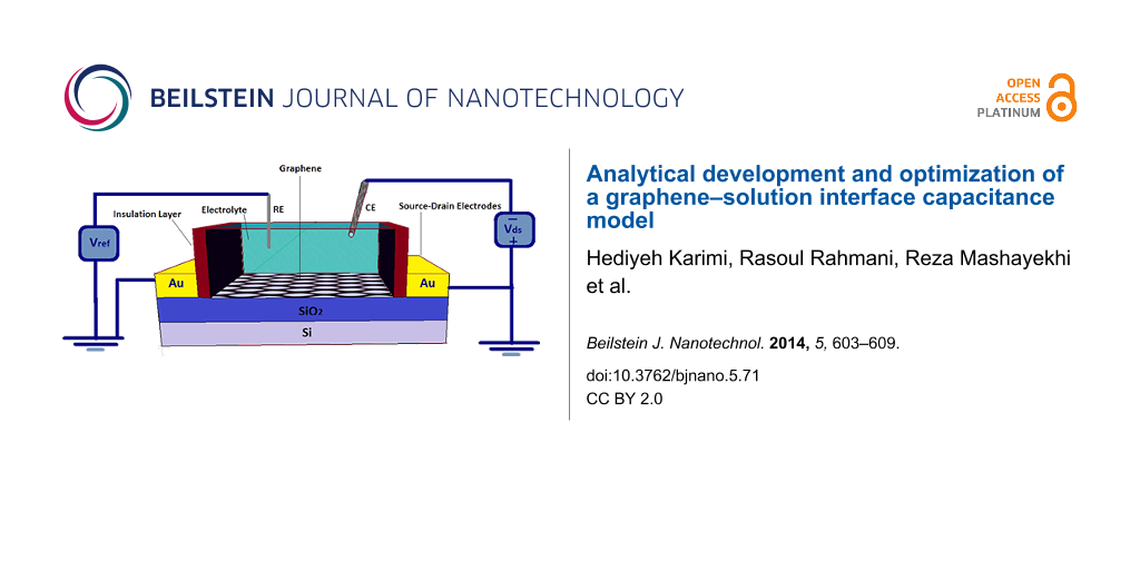
An EGFET fabricated on a SiO2/Si substrate with gold source and drain electrodes and a graphene layer as a conducting channel can be seen in Figure 1. A 300 nm SiO2 layer as a back-gate dielectric has been deposited above the doped silicon substrate. The graphene layer, the gate, and a quasi-reference electrode were covered by a small droplet of ionic liquid [21]. The standard three-electrode electrochemical cell using a potentiostat has measured the interfacial capacitance of the graphene [22]. VG is the voltage applied at the Pt gate electrode, and Vref is the voltage measured on the quasi-reference electrode. Ye et al. have discussed the distinguished properties and high carrier-density transport of ion-gated mono-, bi-, and trilayer graphene bases in double-layer transistors [23]. They demonstrated that Vref ≈ 0 over the whole sweep range of VG, which has led to dropping all the applied VG at the liquid/graphene interface [15].
![[2190-4286-5-71-1]](/bjnano/content/figures/2190-4286-5-71-1.png?scale=2.0&max-width=1024&background=FFFFFF)
Figure 1: A schematic of a graphene-based EGFET including the bias configuration (three-electrode electrochemical cell).
Figure 1: A schematic of a graphene-based EGFET including the bias configuration (three-electrode electrochem...
In order to minimize the background capacitance,the mentioned configuration is employed which can also prevent the graphene edges from exposure to the electrolyte. To interpret the electrical response of the device, an analytical model of the EGFET together with the equivalent circuit describing its operation is discussed in this paper. As depicted in Figure 2, the measured capacitance is assumed as the contribution of two interfacial capacitances which arise from the double layer formed by ions at the graphene–ionic liquid interface and the quantum capacitance of graphene. The particular case of EGFET is discussed in the context of 2D systems.
![[2190-4286-5-71-2]](/bjnano/content/figures/2190-4286-5-71-2.png?scale=2.0&max-width=1024&background=FFFFFF)
Figure 2: A cross-section of graphene-based electrolyte-gated field effect transistor, together with the equivalent electrical circuit.
Figure 2: A cross-section of graphene-based electrolyte-gated field effect transistor, together with the equi...
To substantiate all the consideration just made, the equivalent circuit of the EGFET device is suggested in terms of a simple, well-defined theoretical model. It is seen that C′G is the capacitance that forms between the gate and the ionic liquid, RB is the electrical resistance of the solution, CG represents the geometrical capacitance of the double layer/graphene interface to model the accumulation of a layer of counter-ions on a charged electrode. Finally, CQ is the quantum capacitance of the EGFET associated with the finite density of states of graphene [24]. Figure 2 shows that VG has a strong influence on the capacitance. The total capacitance is given by 1/C = 1/CG + 1/CQ with the smaller of the two capacitances dominating the total capacitance. Previous experimental studies have reported a large geometrical capacitance (several tens of μF∕cm2) [25,26]. Since the two mentioned capacitances are connected in series, the smallest one would dominate the total capacitance. Hence, geometrical capacitance is neglected compared to the theoretically predicted quantum capacitance of graphene. As expected, CQ dominates the total capacitance, which is why the position of the Fermi energy EF can be tuned by applying only small values of VG. These explanations of the current study are consistent with those of Jilin Xia [26] in 2009, who found that the Debye ionic screening length of the ionic liquid is virtually zero, which makes the quantum capacitance a dominant source of the measured capacitance. They performed the measurement of quantum capacitance of bilayer graphene in an ionic liquid electrolyte. The aim of this study is to evaluate the quantum capacitance of single layer graphene sheet as a function of voltage, and validate theoretical predictions with the experimental results [26].
Results and Discussion
Proposed model
The quantum capacitance of nanoscale devices is considered as an important quantity in the design of nanoelectronic devices. The classic expression for quantum capacitance utilized in the prediction of the theoretical model for an ideal single layer graphene [27,28] is
![[2190-4286-5-71-i1]](/bjnano/content/inline/2190-4286-5-71-i1.svg?max-width=590&scale=1.18182)
in which ∂Q = e·∂n is the charge measured in coulombs, e is the electron charge, and n is the intrinsic carrier concentration of graphene. By substitution of the applied voltage ∂V = ∂E/e to the device we obtain
![[2190-4286-5-71-i2]](/bjnano/content/inline/2190-4286-5-71-i2.svg?max-width=590&scale=1.18182)
In the modeling process, the density of state (DOS) and the Fermi probability function, f(E), are employed. It is notable that electrical property of materials from metal to semiconductor is changing by the gradient of DOS(E) near the Dirac point [29].
![[2190-4286-5-71-i3]](/bjnano/content/inline/2190-4286-5-71-i3.svg?max-width=590&scale=1.18182)
where aC-C = 1.42 Å is the carbon–carbon bond length, t = 2.7 eV is the nearest neighbor C–C tight binding overlap energy,
![[Graphic 1]](/bjnano/content/inline/2190-4286-5-71-i16.svg?max-width=637&scale=1.18182)
is the energy band gap of graphene monolayer, and the Fermi probability function f(E) is defined as [30]
![[2190-4286-5-71-i4]](/bjnano/content/inline/2190-4286-5-71-i4.svg?max-width=590&scale=1.18182)
The integral of these two values with respect to E gives the carrier concentration equation as
![[2190-4286-5-71-i5]](/bjnano/content/inline/2190-4286-5-71-i5.svg?max-width=590&scale=1.18182)
By replacing the DOS and f(E) in Equation 3, the carrier concentration in the non-parabolic region is defined as
![[2190-4286-5-71-i6]](/bjnano/content/inline/2190-4286-5-71-i6.svg?max-width=590&scale=1.18182)
Now the quantum capacitance can be calculated as:
![[2190-4286-5-71-i7]](/bjnano/content/inline/2190-4286-5-71-i7.svg?max-width=590&scale=1.18182)
The equation provides a quantitative description of the graphene quantum capacitance in terms of the Fermi velocity [31], carrier density, temperature and fundamental physical quantities. According to the relationship between energy band structure and the graphene potential, the quantum capacitance–voltage characteristic of the proposed model is depicted in Figure 3. In the figure, the experimental data is also plotted to have a fair scale for validating the proposed model [32].
![[2190-4286-5-71-3]](/bjnano/content/figures/2190-4286-5-71-3.png?scale=2.0&max-width=1024&background=FFFFFF)
Figure 3: The proposed model of quantum capacitance of EGFETs based single-layer graphene.
Figure 3: The proposed model of quantum capacitance of EGFETs based single-layer graphene.
To get a greater insight into the quantum capacitance of graphene-based EGFET devices, a number of important characteristics of the C–V curve are discussed. To begin with, at the Dirac point, the quantum capacitance has a minimum value which is close to zero. The other evident aspect in the quantum capacitance model is the linear rise of the capacitance with the voltage, which is symmetric with respect to the Dirac point. Despite of all mentioned vintages of the proposed model, the characteristics of the proposed model diverge considerably from the experimental data. To ease this error, a new function of E is multiplied by the previous model in Equation 7. This function is a square root function, which must be symmetric to its own origin. Otherwise, it will disrupt the isochronism of the proposed model. Equation 8 shows the general form of the suggested function multiplied by the presented model in Equation 7. The quantum capacitance, Cq, is now
![[2190-4286-5-71-i8]](/bjnano/content/inline/2190-4286-5-71-i8.svg?max-width=590&scale=1.18182)
where α and β are unknown parameters, which need to be adjusted properly. Finding the best fitted values for α and β requires an optimization technique with an accurate and reliable performance. To this end, ant colony optimization (ACO) is used as one of the well-known and efficient metaheuristic swarm intelligence-based optimization algorithms. The ACO algorithm has several advantages over conventional mathematic algorithms [33,34]. It is a fast converging algorithm with the capability of escaping from local optima in the search space. The random values used in the movements of the particles help the algorithm to stochastically improve the obtained solution during each iteration.
Ant colony optimization overview
Ant colony optimization (ACO), which is inspired by the foraging behavior of real ant colonies exploring for foods, was proposed by Dorigo in 1992 [33,35,36]. ACO mainly imitates the team work of an ant colony in finding a food source. If an ant finds a food source, it will carry a portion of the food to the nest, after performing some evaluations about the size of the source. On the way back to the nest, it releases some pheromones, which are known as pheromone trail. The rest of the ants in the nest can reach to the food source by tracing the remaining pheromones. The same behavior is shown by the rest of the ants in returning to the nest from the source. The amount of the pheromones deposited on the way is quite dependant on the quantity and quality of the food source [37]. The pheromone (τt) is a vaporizable substance and its amount decreases over time. Therefore, the path with the highest amount of pheromone is the one, which was chosen by the more ants than the other paths. The shortness of the path is a priority to the pheromone trail and the ants try to find the shortest possible path. In the ACO technique, the pheromone trail that represents a better solution, is updated consequently and there exist several ant colony models in the literature [37-39]. Equation 9 presents the location of the k-th ant in the solution space:
![[2190-4286-5-71-i9]](/bjnano/content/inline/2190-4286-5-71-i9.svg?max-width=590&scale=1.18182)
where T is the total number of iterations and t denotes the iteration number, xgbest is the location of the best objective value obtained until iteration t, and ∂x is a random vector generated from [−α, α] to determine the allowed variation the ant can have from the xgbest with the same dimensions. The length of this jump (variation) is obtained from Equation 10 at the end of √T iterations.
![[2190-4286-5-71-i10]](/bjnano/content/inline/2190-4286-5-71-i10.svg?max-width=590&scale=1.18182)
The direction of the variation from xgbest, which is shown by ± in Equation 9 is decided based on the following equation:
![[2190-4286-5-71-i11]](/bjnano/content/inline/2190-4286-5-71-i11.svg?max-width=590&scale=1.18182)
To simulate the evaporation of the pheromone, Equation 12 is presented, and Equation 13 shows the increment of the pheromone around the best objective value obtained after each iteration.
![[2190-4286-5-71-i12]](/bjnano/content/inline/2190-4286-5-71-i12.svg?max-width=590&scale=1.18182)
![[2190-4286-5-71-i13]](/bjnano/content/inline/2190-4286-5-71-i13.svg?max-width=590&scale=1.18182)
Optimization of the proposed model
The aim of the optimization is to find the best values for α and β in Equation 8. Therefore, the search space of the problem is a 2D space, which returns values for α and β at each iteration. The number of ants hired as agents in the ACO algorithm is set to be 100, which requires a matrix of 100 × 2 to store the α and β values for all the ants, at each iteration. To evaluate the solutions proposed at each iteration, a fitness function is defined as:
![[2190-4286-5-71-i14]](/bjnano/content/inline/2190-4286-5-71-i14.svg?max-width=590&scale=1.18182)
where ![[Graphic 2]](/bjnano/content/inline/2190-4286-5-71-i17.svg?max-width=637&scale=1.18182) represents the modelled quantum capacitance waveform for particle i, Cq(k) is the experimental data of the quantum capacitance, and φi is the fitness value for the i-th ant in the colony. The chosen fitness function calculates the squared error between the proposed model and experimental data; hence, the lowest value for the fitness function indicates the best solution to the α and β values. The strategy of the ACO algorithm for the optimization is shown in Figure 4 as a flow chart. The best values obtained for the parameters α and β after the optimization process are shown in Table 1. The fitness value that is the best of 30 runs of the algorithm, and the respective values for the desired parameters are tabulated. Figure 5 shows the proposed single-layer graphene quantum capacitance model, the optimized proposed model and the experimental extracted data, as graphs.
represents the modelled quantum capacitance waveform for particle i, Cq(k) is the experimental data of the quantum capacitance, and φi is the fitness value for the i-th ant in the colony. The chosen fitness function calculates the squared error between the proposed model and experimental data; hence, the lowest value for the fitness function indicates the best solution to the α and β values. The strategy of the ACO algorithm for the optimization is shown in Figure 4 as a flow chart. The best values obtained for the parameters α and β after the optimization process are shown in Table 1. The fitness value that is the best of 30 runs of the algorithm, and the respective values for the desired parameters are tabulated. Figure 5 shows the proposed single-layer graphene quantum capacitance model, the optimized proposed model and the experimental extracted data, as graphs.
![[2190-4286-5-71-4]](/bjnano/content/figures/2190-4286-5-71-4.png?scale=2.0&max-width=1024&background=FFFFFF)
Figure 4: A flowchart of ACO-based algorithm for optimizing the quantum capacitance model.
Figure 4: A flowchart of ACO-based algorithm for optimizing the quantum capacitance model.
![[2190-4286-5-71-5]](/bjnano/content/figures/2190-4286-5-71-5.png?scale=2.0&max-width=1024&background=FFFFFF)
Figure 5: Comparison between the proposed single-layer graphene quantum capacitance model, the optimized proposed model and the experimental extracted data.
Figure 5: Comparison between the proposed single-layer graphene quantum capacitance model, the optimized prop...
To evaluate the quality of the optimized model compared with the experimental data, the mean absolute percentage error (MAPE) is used as an error evaluation parameter, as shown in Equation 15.
![[2190-4286-5-71-i15]](/bjnano/content/inline/2190-4286-5-71-i15.svg?max-width=590&scale=1.18182)
The results for the MAPE for the proposed model and the optimized proposed model are shown in Table 2. The accuracy based on the obtained MAPE value is also reported as the result of subtracting the MAPE from 100 percent. Based on the results tabulated, the accuracy of the optimized model is more than 97%, which is in an acceptable range of accuracy.
The logarithmic convergence profile of the best fitness value obtained is plotted in Figure 6. The graph indicates that the algorithm converges to the optimized values with an acceptable convergence speed after around 1500 iterations.
![[2190-4286-5-71-6]](/bjnano/content/figures/2190-4286-5-71-6.png?scale=2.0&max-width=1024&background=FFFFFF)
Figure 6: The convergence profile of the optimization of the proposed model using ACO technique.
Figure 6: The convergence profile of the optimization of the proposed model using ACO technique.
It is apparent that there is a favorable agreement between the optimized proposed model of graphene-based EGFETs device and experimental result. It can be concluded that, the presented model can be applied as a powerful tool to optimize the graphene-based EGFETs device performance.
Conclusion
Graphene as a 2D sheet of hexagonally arranged carbon atoms exhibits amazing carrier transport properties and a high sensitivity at the single-molecule level, which makes it a promising material for nanoscale devices. According to the graphene structure, it can satisfy the major requirements of a channel in electrolyte-gated transistor (EGFET) devices due to its ballistic transport, high conductivity, and strong mechanical and elasticity properties. An analytical modeling of the graphene capacitance as a major characteristic of EGFET is studied in this paper and the electrical circuit of the device is discussed. An EGFET based structure is employed as a platform and the graphene capacitance is studied. In order to enhance the accuracy of the proposed model, an ant colony optimization (ACO) algorithm is implemented and we obtained acceptable results with more than 97% of accuracy. Finally, for the purpose of verification, the C–V characteristic of the optimized model is investigated with an existing experimental study and shows an acceptable agreement. This paper demonstrates how the optimized model can be used to predict the capacitance variation of graphene in graphene-based devices.
Acknowledgements
The authors would like to acknowledge the financial support from Research University grant of the Ministry of Education Malaysia under project number Q.J130000.2523.04H99. Also thanks to the Research Management Centre (RMC) of Universiti Teknologi Malaysia (UTM) for providing an excellent research environment in which this work was completed.
References
-
Gibertini, M.; Singha, A.; Pellegrini, V.; Polini, M.; Vignale, G.; Pinczuk, A.; Pfeiffer, L. N.; West, K. W. Phys. Rev. B 2009, 79, 241406. doi:10.1103/PhysRevB.79.241406
Return to citation in text: [1] -
Zârbo, L. P.; Nikolić, B. K. EPL 2007, 80, 47001. doi:10.1209/0295-5075/80/47001
Return to citation in text: [1] -
Burgess, C. P.; Dolan, B. P. Phys. Rev. B 2007, 76, 113406. doi:10.1103/PhysRevB.76.113406
Return to citation in text: [1] -
Wang, X.; Xie, W.; Xu, J.-B. Adv. Mater., in press. doi:10.1002/adma.201306041
Return to citation in text: [1] -
Zou, Y.; Li, F.; Zhu, Z. H.; Zhao, M. W.; Xu, X. G.; Su, X. Y. Eur. Phys. J. B 2011, 81, 475–479. doi:10.1140/epjb/e2011-20225-8
Return to citation in text: [1] -
Chai, Y.; Gong, J.; Zhang, K.; Chan, P. C. H.; Yuen, M. M. F. Nanotechnology 2007, 18, 355709. doi:10.1088/0957-4484/18/35/355709
Return to citation in text: [1] -
Novoselov, K. S.; Geim, A. K.; Morozov, S. V.; Jiang, D.; Zhang, Y.; Dubonos, S. V.; Grigorieva, I. V.; Firsov, A. A. Science 2004, 306, 666–669. doi:10.1126/science.1102896
Return to citation in text: [1] [2] -
Dong, X.; Zhao, X.; Wang, L.; Huang, W. Curr. Phys. Chem. 2013, 3, 291–301. doi:10.2174/1877946811303030006
Return to citation in text: [1] -
Ragheb, T.; Massoud, Y. On the modeling of resistance in graphene nanoribbon (GNR) for future interconnect applications. In IEEE/ACM International Conference on Computer-Aided Design, 2008. ICCAD 2008, San Jose, CA, Nov 10–13, 2008; IEEE, 2008; pp 593–597. doi:10.1109/ICCAD.2008.4681637
Return to citation in text: [1] -
Adam, S.; Das Sarma, S. Phys. Rev. B 2008, 77, 115436. doi:10.1103/PhysRevB.77.115436
Return to citation in text: [1] -
Hill, E. W.; Geim, A. K.; Novoselov, K.; Schedin, F.; Blake, P. IEEE Trans. Magn. 2006, 42, 2694–2696. doi:10.1109/TMAG.2006.878852
Return to citation in text: [1] -
Grassi, R.; Gnudi, A.; Gnani, E.; Reggiani, S.; Baccarani, G. Graphene Nanoribbons FETs for High-Performance Logic Applications: Perspectives and Challenges. In 9th International Conference on Solid-State and Integrated-Circuit Technology, 2008. ICSICT 2008, Solid-State and Integrated-Circuit Technology, Beijing, China, Oct 20–23, 2008; IEEE, 2008; pp 365–368. doi:10.1109/ICSICT.2008.4734555
Return to citation in text: [1] -
Liang, G.; Neophytou, N.; Nikonov, D. E.; Lundstrom, M. S. IEEE Trans. Electron Devices 2007, 54, 677–682. doi:10.1109/TED.2007.891872
Return to citation in text: [1] -
Bolotin, K. I.; Sikes, K. J.; Jiang, Z.; Klima, M.; Fudenberg, G.; Hone, J.; Kim, P.; Stormer, H. L. Solid State Commun. 2008, 146, 351–355. doi:10.1016/j.ssc.2008.02.024
Return to citation in text: [1] -
Chen, D.; Tang, L.; Li, J. Chem. Soc. Rev. 2010, 39, 3157–3180. doi:10.1039/b923596e
Return to citation in text: [1] [2] [3] -
Novoselov, K. S.; Fal′ko, V. I.; Colombo, L.; Gellert, P. R.; Schwab, M. G.; Kim, K. Nature 2012, 490, 192–200. doi:10.1038/nature11458
Return to citation in text: [1] -
Neto, A. C.; Geim, A. New Sci. 2012, 2012, 214.
Return to citation in text: [1] -
Han, M. Y.; Özyilmaz, B.; Zhang, Y.; Kim, P. Phys. Rev. Lett. 2007, 98, 206805. doi:10.1103/PhysRevLett.98.206805
Return to citation in text: [1] -
Yang, L.; Park, C.-H.; Son, Y.-W.; Cohen, M. L.; Louie, S. G. Phys. Rev. Lett. 2007, 99, 186801. doi:10.1103/PhysRevLett.99.186801
Return to citation in text: [1] -
Novoselov, K. S.; Jiang, D.; Schedin, F.; Booth, T. J.; Khotkevich, V. V.; Morozov, S. V.; Geim, A. K. Proc. Natl. Acad. Sci. U. S. A. 2005, 102, 10451–10453. doi:10.1073/pnas.0502848102
Return to citation in text: [1] -
Ouyang, Y.; Yoon, Y.; Guo, J. IEEE Trans. Electron Devices 2007, 54, 2223–2231. doi:10.1109/TED.2007.902692
Return to citation in text: [1] -
Heller, I.; Chatoor, S.; Männik, J.; Zevenbergen, M. A. G.; Dekker, C.; Lemay, S. G. J. Am. Chem. Soc. 2010, 132, 17149–17156. doi:10.1021/ja104850n
Return to citation in text: [1] -
Ye, J.; Craciun, M. F.; Koshino, M.; Russo, S.; Inoue, S.; Yuan, H.; Shimotani, H.; Morpurgo, A. F.; Iwasa, Y. Proc. Natl. Acad. Sci. U. S. A. 2011, 108, 13002–13006. doi:10.1073/pnas.1018388108
Return to citation in text: [1] -
Warner, J. H.; Rümmeli, M. H.; Ge, L.; Gemming, T.; Montanari, B.; Harrison, N. M.; Büchner, B.; Briggs, G. A. D. Nat. Nanotechnol. 2009, 4, 500–504. doi:10.1038/nnano.2009.194
Return to citation in text: [1] -
Sorgenfrei, S.; Chiu, C.-y.; Gonzalez, R. L., Jr.; Yu, Y.-J.; Kim, P.; Nuckolls, C.; Shepard, K. L. Nat. Nanotechnol. 2011, 6, 126–132. doi:10.1038/nnano.2010.275
Return to citation in text: [1] -
O'Connor, I.; Junchen, L.; Gaffiot, F.; Prégaldiny, F.; Lallement, C.; Maneux, C.; Goguet, J.; Frégonèse, S.; Zimmer, T.; Anghel, L.; Trong-Trinh, D.; Leveugle, R. IEEE Trans. Circuits Syst., I 2007, 54, 2365–2379. doi:10.1109/TCSI.2007.907835
Return to citation in text: [1] [2] [3] -
John, D. L.; Castro, L. C.; Pulfrey, D. L. J. Appl. Phys. 2004, 96, 5180–5184. doi:10.1063/1.1803614
Return to citation in text: [1] -
Chu, L.; Xue, Q.; Zhang, T.; Ling, C. J. Phys. Chem. C 2011, 115, 15217–15224. doi:10.1021/jp2030768
Return to citation in text: [1] -
Schaper, A. K.; Wang, M. S.; Xu, Z.; Bando, Y.; Golberg, D. Nano Lett. 2011, 11, 3295–3300. doi:10.1021/nl201655c
Return to citation in text: [1] -
Karimi, F. A. H.; Ahmadi, M. T.; Rahmani, M.; Akbari, E.; Kiani, M. J.; Khalid, M. Sci. Adv. Mater. 2012, 4, 1142–1147. doi:10.1166/sam.2012.1405
Return to citation in text: [1] -
Venkatesan, B. M.; Bashir, R. Nat. Nanotechnol. 2011, 6, 615–624. doi:10.1038/nnano.2011.129
Return to citation in text: [1] -
Xia, J.; Chen, F.; Li, J.; Tao, N. Nat. Nanotechnol. 2009, 4, 505–509. doi:10.1038/nnano.2009.177
Return to citation in text: [1] -
Dorigo, M.; Birattari, M.; Stutzle, T. IEEE Comput. Intell. Mag. 2006, 1, 28–39. doi:10.1109/MCI.2006.329691
Return to citation in text: [1] [2] -
Dorigo, M.; Blum, C. Theor. Comp. Sci. 2005, 344, 243–278. doi:10.1016/j.tcs.2005.05.020
Return to citation in text: [1] -
Dorigo, M.; Gambardella, L. M. IEEE Trans. Evol. Comput. 1997, 1, 53–66. doi:10.1109/4235.585892
Return to citation in text: [1] -
Shen, Q.; Jiang, J.-H.; Tao, J.-c.; Shen, G.-l.; Yu, R.-Q. J. Chem. Inf. Model. 2005, 45, 1024–1029. doi:10.1021/ci049610z
Return to citation in text: [1] -
Socha, K.; Dorigo, M. Eur. J. Oper. Res. 2008, 185, 1155–1173. doi:10.1016/j.ejor.2006.06.046
Return to citation in text: [1] [2] -
Dorigo, M.; Maniezzo, V.; Colorni, A. IEEE Trans. Syst. Man Cybern., Part B 1996, 26, 29–41. doi:10.1109/3477.484436
Return to citation in text: [1] -
Rahmani, R.; Yusof, R.; Seyedmahmoudian, M.; Mekhilef, S. J. Wind End. Ind. Aerodyn. 2013, 123, Part A, 163–170. doi:10.1016/j.jweia.2013.10.004
Return to citation in text: [1]
| 1. | Gibertini, M.; Singha, A.; Pellegrini, V.; Polini, M.; Vignale, G.; Pinczuk, A.; Pfeiffer, L. N.; West, K. W. Phys. Rev. B 2009, 79, 241406. doi:10.1103/PhysRevB.79.241406 |
| 2. | Zârbo, L. P.; Nikolić, B. K. EPL 2007, 80, 47001. doi:10.1209/0295-5075/80/47001 |
| 3. | Burgess, C. P.; Dolan, B. P. Phys. Rev. B 2007, 76, 113406. doi:10.1103/PhysRevB.76.113406 |
| 4. | Wang, X.; Xie, W.; Xu, J.-B. Adv. Mater., in press. doi:10.1002/adma.201306041 |
| 5. | Zou, Y.; Li, F.; Zhu, Z. H.; Zhao, M. W.; Xu, X. G.; Su, X. Y. Eur. Phys. J. B 2011, 81, 475–479. doi:10.1140/epjb/e2011-20225-8 |
| 6. | Chai, Y.; Gong, J.; Zhang, K.; Chan, P. C. H.; Yuen, M. M. F. Nanotechnology 2007, 18, 355709. doi:10.1088/0957-4484/18/35/355709 |
| 7. | Novoselov, K. S.; Geim, A. K.; Morozov, S. V.; Jiang, D.; Zhang, Y.; Dubonos, S. V.; Grigorieva, I. V.; Firsov, A. A. Science 2004, 306, 666–669. doi:10.1126/science.1102896 |
| 14. | Bolotin, K. I.; Sikes, K. J.; Jiang, Z.; Klima, M.; Fudenberg, G.; Hone, J.; Kim, P.; Stormer, H. L. Solid State Commun. 2008, 146, 351–355. doi:10.1016/j.ssc.2008.02.024 |
| 24. | Warner, J. H.; Rümmeli, M. H.; Ge, L.; Gemming, T.; Montanari, B.; Harrison, N. M.; Büchner, B.; Briggs, G. A. D. Nat. Nanotechnol. 2009, 4, 500–504. doi:10.1038/nnano.2009.194 |
| 12. | Grassi, R.; Gnudi, A.; Gnani, E.; Reggiani, S.; Baccarani, G. Graphene Nanoribbons FETs for High-Performance Logic Applications: Perspectives and Challenges. In 9th International Conference on Solid-State and Integrated-Circuit Technology, 2008. ICSICT 2008, Solid-State and Integrated-Circuit Technology, Beijing, China, Oct 20–23, 2008; IEEE, 2008; pp 365–368. doi:10.1109/ICSICT.2008.4734555 |
| 13. | Liang, G.; Neophytou, N.; Nikonov, D. E.; Lundstrom, M. S. IEEE Trans. Electron Devices 2007, 54, 677–682. doi:10.1109/TED.2007.891872 |
| 25. | Sorgenfrei, S.; Chiu, C.-y.; Gonzalez, R. L., Jr.; Yu, Y.-J.; Kim, P.; Nuckolls, C.; Shepard, K. L. Nat. Nanotechnol. 2011, 6, 126–132. doi:10.1038/nnano.2010.275 |
| 26. | O'Connor, I.; Junchen, L.; Gaffiot, F.; Prégaldiny, F.; Lallement, C.; Maneux, C.; Goguet, J.; Frégonèse, S.; Zimmer, T.; Anghel, L.; Trong-Trinh, D.; Leveugle, R. IEEE Trans. Circuits Syst., I 2007, 54, 2365–2379. doi:10.1109/TCSI.2007.907835 |
| 8. | Dong, X.; Zhao, X.; Wang, L.; Huang, W. Curr. Phys. Chem. 2013, 3, 291–301. doi:10.2174/1877946811303030006 |
| 9. | Ragheb, T.; Massoud, Y. On the modeling of resistance in graphene nanoribbon (GNR) for future interconnect applications. In IEEE/ACM International Conference on Computer-Aided Design, 2008. ICCAD 2008, San Jose, CA, Nov 10–13, 2008; IEEE, 2008; pp 593–597. doi:10.1109/ICCAD.2008.4681637 |
| 10. | Adam, S.; Das Sarma, S. Phys. Rev. B 2008, 77, 115436. doi:10.1103/PhysRevB.77.115436 |
| 11. | Hill, E. W.; Geim, A. K.; Novoselov, K.; Schedin, F.; Blake, P. IEEE Trans. Magn. 2006, 42, 2694–2696. doi:10.1109/TMAG.2006.878852 |
| 23. | Ye, J.; Craciun, M. F.; Koshino, M.; Russo, S.; Inoue, S.; Yuan, H.; Shimotani, H.; Morpurgo, A. F.; Iwasa, Y. Proc. Natl. Acad. Sci. U. S. A. 2011, 108, 13002–13006. doi:10.1073/pnas.1018388108 |
| 7. | Novoselov, K. S.; Geim, A. K.; Morozov, S. V.; Jiang, D.; Zhang, Y.; Dubonos, S. V.; Grigorieva, I. V.; Firsov, A. A. Science 2004, 306, 666–669. doi:10.1126/science.1102896 |
| 15. | Chen, D.; Tang, L.; Li, J. Chem. Soc. Rev. 2010, 39, 3157–3180. doi:10.1039/b923596e |
| 19. | Yang, L.; Park, C.-H.; Son, Y.-W.; Cohen, M. L.; Louie, S. G. Phys. Rev. Lett. 2007, 99, 186801. doi:10.1103/PhysRevLett.99.186801 |
| 21. | Ouyang, Y.; Yoon, Y.; Guo, J. IEEE Trans. Electron Devices 2007, 54, 2223–2231. doi:10.1109/TED.2007.902692 |
| 18. | Han, M. Y.; Özyilmaz, B.; Zhang, Y.; Kim, P. Phys. Rev. Lett. 2007, 98, 206805. doi:10.1103/PhysRevLett.98.206805 |
| 22. | Heller, I.; Chatoor, S.; Männik, J.; Zevenbergen, M. A. G.; Dekker, C.; Lemay, S. G. J. Am. Chem. Soc. 2010, 132, 17149–17156. doi:10.1021/ja104850n |
| 15. | Chen, D.; Tang, L.; Li, J. Chem. Soc. Rev. 2010, 39, 3157–3180. doi:10.1039/b923596e |
| 16. | Novoselov, K. S.; Fal′ko, V. I.; Colombo, L.; Gellert, P. R.; Schwab, M. G.; Kim, K. Nature 2012, 490, 192–200. doi:10.1038/nature11458 |
| 17. | Neto, A. C.; Geim, A. New Sci. 2012, 2012, 214. |
| 15. | Chen, D.; Tang, L.; Li, J. Chem. Soc. Rev. 2010, 39, 3157–3180. doi:10.1039/b923596e |
| 20. | Novoselov, K. S.; Jiang, D.; Schedin, F.; Booth, T. J.; Khotkevich, V. V.; Morozov, S. V.; Geim, A. K. Proc. Natl. Acad. Sci. U. S. A. 2005, 102, 10451–10453. doi:10.1073/pnas.0502848102 |
| 27. | John, D. L.; Castro, L. C.; Pulfrey, D. L. J. Appl. Phys. 2004, 96, 5180–5184. doi:10.1063/1.1803614 |
| 28. | Chu, L.; Xue, Q.; Zhang, T.; Ling, C. J. Phys. Chem. C 2011, 115, 15217–15224. doi:10.1021/jp2030768 |
| 26. | O'Connor, I.; Junchen, L.; Gaffiot, F.; Prégaldiny, F.; Lallement, C.; Maneux, C.; Goguet, J.; Frégonèse, S.; Zimmer, T.; Anghel, L.; Trong-Trinh, D.; Leveugle, R. IEEE Trans. Circuits Syst., I 2007, 54, 2365–2379. doi:10.1109/TCSI.2007.907835 |
| 26. | O'Connor, I.; Junchen, L.; Gaffiot, F.; Prégaldiny, F.; Lallement, C.; Maneux, C.; Goguet, J.; Frégonèse, S.; Zimmer, T.; Anghel, L.; Trong-Trinh, D.; Leveugle, R. IEEE Trans. Circuits Syst., I 2007, 54, 2365–2379. doi:10.1109/TCSI.2007.907835 |
| 37. | Socha, K.; Dorigo, M. Eur. J. Oper. Res. 2008, 185, 1155–1173. doi:10.1016/j.ejor.2006.06.046 |
| 37. | Socha, K.; Dorigo, M. Eur. J. Oper. Res. 2008, 185, 1155–1173. doi:10.1016/j.ejor.2006.06.046 |
| 38. | Dorigo, M.; Maniezzo, V.; Colorni, A. IEEE Trans. Syst. Man Cybern., Part B 1996, 26, 29–41. doi:10.1109/3477.484436 |
| 39. | Rahmani, R.; Yusof, R.; Seyedmahmoudian, M.; Mekhilef, S. J. Wind End. Ind. Aerodyn. 2013, 123, Part A, 163–170. doi:10.1016/j.jweia.2013.10.004 |
| 33. | Dorigo, M.; Birattari, M.; Stutzle, T. IEEE Comput. Intell. Mag. 2006, 1, 28–39. doi:10.1109/MCI.2006.329691 |
| 34. | Dorigo, M.; Blum, C. Theor. Comp. Sci. 2005, 344, 243–278. doi:10.1016/j.tcs.2005.05.020 |
| 33. | Dorigo, M.; Birattari, M.; Stutzle, T. IEEE Comput. Intell. Mag. 2006, 1, 28–39. doi:10.1109/MCI.2006.329691 |
| 35. | Dorigo, M.; Gambardella, L. M. IEEE Trans. Evol. Comput. 1997, 1, 53–66. doi:10.1109/4235.585892 |
| 36. | Shen, Q.; Jiang, J.-H.; Tao, J.-c.; Shen, G.-l.; Yu, R.-Q. J. Chem. Inf. Model. 2005, 45, 1024–1029. doi:10.1021/ci049610z |
| 31. | Venkatesan, B. M.; Bashir, R. Nat. Nanotechnol. 2011, 6, 615–624. doi:10.1038/nnano.2011.129 |
| 32. | Xia, J.; Chen, F.; Li, J.; Tao, N. Nat. Nanotechnol. 2009, 4, 505–509. doi:10.1038/nnano.2009.177 |
| 29. | Schaper, A. K.; Wang, M. S.; Xu, Z.; Bando, Y.; Golberg, D. Nano Lett. 2011, 11, 3295–3300. doi:10.1021/nl201655c |
| 30. | Karimi, F. A. H.; Ahmadi, M. T.; Rahmani, M.; Akbari, E.; Kiani, M. J.; Khalid, M. Sci. Adv. Mater. 2012, 4, 1142–1147. doi:10.1166/sam.2012.1405 |
© 2014 Karimi et al; licensee Beilstein-Institut.
This is an Open Access article under the terms of the Creative Commons Attribution License (http://creativecommons.org/licenses/by/2.0), which permits unrestricted use, distribution, and reproduction in any medium, provided the original work is properly cited.
The license is subject to the Beilstein Journal of Nanotechnology terms and conditions: (http://www.beilstein-journals.org/bjnano)