Abstract
There have recently been several experiments studying induced superconductivity in semiconducting two-dimensional electron gases that are strongly coupled to thin superconducting layers, as well as probing possible topological phases supporting Majorana bound states in such setups. We show that a large band shift is induced in the semiconductor by the superconductor in this geometry, thus making it challenging to realize a topological phase. Additionally, we show that while increasing the thickness of the superconducting layer reduces the magnitude of the band shift, it also leads to a more significant renormalization of the semiconducting material parameters and does not reduce the challenge of tuning into a topological phase.
Introduction
Topological superconductors host zero-energy Majorana bound states at their edges that are highly sought for applications in topological quantum computing [1-3]. The two proposals to realize topological superconductivity that have received the most attention to date involve engineering Majorana bound states in either low-dimensional semiconducting systems [4-23] or in ferromagnetic atomic chains [24-32]. After the first signatures of topological superconductivity were observed [33-37], much of the experimental focus was placed on developing more suitable devices for realizing robust topological superconducting phases. One of the most significant experimental advances of the past few years was the successful epitaxial growth of thin layers of superconducting Al on InAs and InSb nanowires [38-42]. The intimate contact between the semiconductor and superconductor in these devices ensures a hard induced superconducting gap. Recently, this epitaxial growth technique has been applied also to InAs two-dimensional electron gases (2DEGs) [43-47].
The proximity effect has been theoretically studied recently in both strictly one-dimensional (1D) [48] and quasi-1D [49] wires coupled to thin superconducting layers. In both instances, a strong proximity coupling induces a large band shift on the semiconducting wire. This band shift is comparable to the level spacing in the superconductor, ![[Graphic 1]](/bjnano/content/inline/2190-4286-9-118-i28.svg?max-width=637&scale=1.18182) (which is δEs ~ 400 meV for a superconductor thickness of d ~ 10 nm and a Fermi velocity of Al of vF ~ 2 × 10⁶ m/s). In both cases, this large band shift makes it very challenging to realize a topological phase when utilizing thin superconducting layers.
(which is δEs ~ 400 meV for a superconductor thickness of d ~ 10 nm and a Fermi velocity of Al of vF ~ 2 × 10⁶ m/s). In both cases, this large band shift makes it very challenging to realize a topological phase when utilizing thin superconducting layers.
In this paper, we extend the works of [48,49] to the 2D limit. We show that the large band shift that plagues the 1D case persists also in two dimensions. First, we show that the self-energy induced in an infinite 2DEG coupled to a superconductor of finite thickness is equivalent to that induced in an infinite wire coupled to a 2D superconductor of finite width (corresponding to the theoretical model of [48]), with the simple replacement of a 1D momentum by the magnitude of a 2D momentum. Analyzing the self-energy, we find that the induced gap in the presence of only Rashba spin–orbit coupling can be made comparable to the bulk gap of the superconductor only if the tunneling energy scale exceeds the large level spacing of the superconducting layer. As in the 1D case, the large tunneling energy scale induces a large band shift on the 2DEG and makes it very challenging to realize a topological phase. We also show that while the band shift can be significantly reduced by increasing the thickness of the superconducting layer, the topological phase is still difficult to realize if the 2DEG/superconductor interface remains very transparent.
Model of the Proximity Effect
The system we consider consists of a 2DEG with strong Rashba spin–orbit interaction (SOI) proximity-coupled to an s-wave superconductor of thickness d, as shown in Figure 1. The 2DEG-superconductor heterostructure is described by the action
![[2190-4286-9-118-i1]](/bjnano/content/inline/2190-4286-9-118-i1.svg?max-width=590&scale=1.18182)
The action of the 2DEG in Nambu space is given by
![[2190-4286-9-118-i2]](/bjnano/content/inline/2190-4286-9-118-i2.svg?max-width=590&scale=1.18182)
where ω is a Matsubara frequency, k = (kx,ky) is the momentum,
![[Graphic 2]](/bjnano/content/inline/2190-4286-9-118-i29.svg?max-width=637&scale=1.18182)
and
![[Graphic 3]](/bjnano/content/inline/2190-4286-9-118-i30.svg?max-width=637&scale=1.18182)
is a spinor of Heisenberg operators describing states in the 2DEG. The Hamiltonian density is
![[2190-4286-9-118-i3]](/bjnano/content/inline/2190-4286-9-118-i3.svg?max-width=590&scale=1.18182)
where ξk = k2/2m2D − μ2D (m2D and μ2D are the effective mass and chemical potential of the 2DEG, respectively, and ![[Graphic 4]](/bjnano/content/inline/2190-4286-9-118-i31.svg?max-width=637&scale=1.18182) ), α is the Rashba SOI constant, and σx,y,z (τx,y,z) are Pauli matrices acting in spin (Nambu) space. The superconductor is described by the BCS action,
), α is the Rashba SOI constant, and σx,y,z (τx,y,z) are Pauli matrices acting in spin (Nambu) space. The superconductor is described by the BCS action,
![[2190-4286-9-118-i4]](/bjnano/content/inline/2190-4286-9-118-i4.svg?max-width=590&scale=1.18182)
where
![[Graphic 5]](/bjnano/content/inline/2190-4286-9-118-i32.svg?max-width=637&scale=1.18182)
is a spinor of Heisenberg operators describing states in the superconductor and the Hamiltonian density is
![[2190-4286-9-118-i5]](/bjnano/content/inline/2190-4286-9-118-i5.svg?max-width=590&scale=1.18182)
with ms, μs, and Δ the effective mass, chemical potential, and pairing potential of the superconductor, respectively. Local tunneling at the interface between the two materials is assumed to conserve both spin and momentum,
![[2190-4286-9-118-i6]](/bjnano/content/inline/2190-4286-9-118-i6.svg?max-width=590&scale=1.18182)
where t is the tunneling amplitude. We must take the 2DEG to be located at some finite z2D (0 < z2D < d) due to the breakdown of the tunneling Hamiltonian approach for the case where the 2DEG is located at the boundary of the superconductor. The breakdown of the tunneling Hamiltonian results from our neglect of the thickness of the 2DEG (for related calculations in which the finite thickness is taken into account, see [50-53]). However, as shown in [48], choosing ![[Graphic 6]](/bjnano/content/inline/2190-4286-9-118-i33.svg?max-width=637&scale=1.18182) (where
(where ![[Graphic 7]](/bjnano/content/inline/2190-4286-9-118-i34.svg?max-width=637&scale=1.18182) is the Fermi momentum of the superconductor) yields good agreement with numerical calculations in which there is no issue with placing the 2DEG strictly at the boundary.
is the Fermi momentum of the superconductor) yields good agreement with numerical calculations in which there is no issue with placing the 2DEG strictly at the boundary.
![[2190-4286-9-118-1]](/bjnano/content/figures/2190-4286-9-118-1.png?scale=2.0&max-width=1024&background=FFFFFF)
Figure 1: A 2DEG is proximity-coupled to an s-wave superconductor with finite thickness d. Both systems are taken to be infinite in the xy-plane.
Figure 1: A 2DEG is proximity-coupled to an s-wave superconductor with finite thickness d. Both systems are t...
In the absence of tunneling, the spectrum of the 2DEG consists of two spin–orbit-split subbands described by
![[2190-4286-9-118-i7]](/bjnano/content/inline/2190-4286-9-118-i7.svg?max-width=590&scale=1.18182)
When the finite-size quantization scale of the superconductor greatly exceeds the gap, ![[Graphic 8]](/bjnano/content/inline/2190-4286-9-118-i35.svg?max-width=637&scale=1.18182) , the first few subbands of the superconductor follow a linearized form given by (
, the first few subbands of the superconductor follow a linearized form given by (![[Graphic 9]](/bjnano/content/inline/2190-4286-9-118-i36.svg?max-width=637&scale=1.18182) )
)
![[2190-4286-9-118-i8]](/bjnano/content/inline/2190-4286-9-118-i8.svg?max-width=590&scale=1.18182)
where δEs = πvF/d is the level spacing in the superconductor (vF = kF/ms is the Fermi velocity) and ![[Graphic 10]](/bjnano/content/inline/2190-4286-9-118-i37.svg?max-width=637&scale=1.18182) . When the thickness of the superconducting layer is much smaller than its coherence length,
. When the thickness of the superconducting layer is much smaller than its coherence length, ![[Graphic 11]](/bjnano/content/inline/2190-4286-9-118-i38.svg?max-width=637&scale=1.18182) = πvF/Δ, the level spacing of the layer greatly exceeds its gap,
= πvF/Δ, the level spacing of the layer greatly exceeds its gap, ![[Graphic 12]](/bjnano/content/inline/2190-4286-9-118-i39.svg?max-width=637&scale=1.18182) .
.
The spectra of the 2DEG and the superconductor are plotted in Figure 2. Provided that ![[Graphic 13]](/bjnano/content/inline/2190-4286-9-118-i40.svg?max-width=637&scale=1.18182) , the bands of the 2DEG and superconductor intersect at high energies
, the bands of the 2DEG and superconductor intersect at high energies ![[Graphic 14]](/bjnano/content/inline/2190-4286-9-118-i41.svg?max-width=637&scale=1.18182) . Since we impose momentum conservation (in addition to energy conservation) in Equation 6, the subbands are coupled only at the intersection points. Thus, a weak tunnel coupling induces anticrossings in the spectrum, as indicated in Figure 2, which leads to a shift in the subbands of the 2DEG. Additionally, the tunnel coupling opens a superconducting gap at the Fermi momenta of the 2DEG; however, due to the intersection points lying at very large energies, the gap opened in the 2DEG is very small. A large gap can only be induced if tunneling is strong enough to overcome the large energy mismatch similar to δEs.
. Since we impose momentum conservation (in addition to energy conservation) in Equation 6, the subbands are coupled only at the intersection points. Thus, a weak tunnel coupling induces anticrossings in the spectrum, as indicated in Figure 2, which leads to a shift in the subbands of the 2DEG. Additionally, the tunnel coupling opens a superconducting gap at the Fermi momenta of the 2DEG; however, due to the intersection points lying at very large energies, the gap opened in the 2DEG is very small. A large gap can only be induced if tunneling is strong enough to overcome the large energy mismatch similar to δEs.
![[2190-4286-9-118-2]](/bjnano/content/figures/2190-4286-9-118-2.png?scale=2.0&max-width=1024&background=FFFFFF)
Figure 2:
Sketch of Bogoliubov excitation spectra as a function of ![[Graphic 15]](/bjnano/content/inline/2190-4286-9-118-i42.svg?max-width=637&scale=1.18182) in the absence of tunneling, assuming
in the absence of tunneling, assuming ![[Graphic 16]](/bjnano/content/inline/2190-4286-9-118-i43.svg?max-width=637&scale=1.18182) and μ2D = 0. The red and blue curves correspond to ± subbands of the 2DEG (Equation 7), respectively, which result from the spin-splitting Rashba SOI. The black curve corresponds to the lowest-energy subband of the superconductor (Equation 8). A weak tunneling amplitude t induces anticrossings in the spectrum where indicated and induces a superconducting gap in the 2DEG at the Fermi momenta (corresponding to those momenta for which E±(k)=0). Due to the large energy mismatch between the superconducting subband and the Fermi points of the 2DEG, the induced gap is very small.
and μ2D = 0. The red and blue curves correspond to ± subbands of the 2DEG (Equation 7), respectively, which result from the spin-splitting Rashba SOI. The black curve corresponds to the lowest-energy subband of the superconductor (Equation 8). A weak tunneling amplitude t induces anticrossings in the spectrum where indicated and induces a superconducting gap in the 2DEG at the Fermi momenta (corresponding to those momenta for which E±(k)=0). Due to the large energy mismatch between the superconducting subband and the Fermi points of the 2DEG, the induced gap is very small.
Figure 2:
Sketch of Bogoliubov excitation spectra as a function of in the absence of tunneling, assuming an...
To determine the self-energy of the 2DEG induced by the superconductor, we integrate out the superconducting degrees of freedom. After integrating out, the 2DEG can be described by the effective action
![[2190-4286-9-118-i9]](/bjnano/content/inline/2190-4286-9-118-i9.svg?max-width=590&scale=1.18182)
with the self-energy given by
![[2190-4286-9-118-i10]](/bjnano/content/inline/2190-4286-9-118-i10.svg?max-width=590&scale=1.18182)
In Equation 10, ![[Graphic 17]](/bjnano/content/inline/2190-4286-9-118-i44.svg?max-width=637&scale=1.18182) is the Green’s function of the bare superconductor (in the absence of tunneling), which satisfies
is the Green’s function of the bare superconductor (in the absence of tunneling), which satisfies
![[2190-4286-9-118-i11]](/bjnano/content/inline/2190-4286-9-118-i11.svg?max-width=590&scale=1.18182)
Imposing a vanishing boundary condition at z = 0 and z = d, we find a solution to Equation 11 given by
![[2190-4286-9-118-i12]](/bjnano/content/inline/2190-4286-9-118-i12.svg?max-width=590&scale=1.18182)
where ![[Graphic 18]](/bjnano/content/inline/2190-4286-9-118-i45.svg?max-width=637&scale=1.18182) = 2ms(μs ± iΩ) − k2 and Ω2 = Δ2 + ω2 [48,54]. The Green’s function of a bulk superconductor, expressed in real space, is
= 2ms(μs ± iΩ) − k2 and Ω2 = Δ2 + ω2 [48,54]. The Green’s function of a bulk superconductor, expressed in real space, is
![[2190-4286-9-118-i13]](/bjnano/content/inline/2190-4286-9-118-i13.svg?max-width=590&scale=1.18182)
where, in evaluating the integral, we make a semiclassical expansion k± = kFφ ± iΩ/(vFφ) ≡ ζ ± iχ (valid in the limit ![[Graphic 19]](/bjnano/content/inline/2190-4286-9-118-i46.svg?max-width=637&scale=1.18182) ) and define a quantity
) and define a quantity ![[Graphic 20]](/bjnano/content/inline/2190-4286-9-118-i47.svg?max-width=637&scale=1.18182) that parametrizes the trajectories of states in the superconductor. Substituting the Green’s function (Equation 12) into the self-energy (Equation 10), we find
that parametrizes the trajectories of states in the superconductor. Substituting the Green’s function (Equation 12) into the self-energy (Equation 10), we find
![[2190-4286-9-118-i14]](/bjnano/content/inline/2190-4286-9-118-i14.svg?max-width=590&scale=1.18182)
where we define
![[2190-4286-9-118-i15]](/bjnano/content/inline/2190-4286-9-118-i15.svg?max-width=590&scale=1.18182)
with γ = t2/vF, an energy scale determined by the tunneling strength. The quantity Γk,ω can be interpreted as an effective quasiparticle weight, as it takes values of 0 < Γ < 1, and is responsible for inducing superconductivity in the 2DEG, while δμk,ω corresponds to a tunneling-induced shift in the effective chemical potential of the 2DEG. Quite surprisingly, the self-energy in Equation 14 and Equation 15 coincides with that of a nanowire coupled to a two-dimensional superconductor with finite width as found in [48], with the simple replacement of a 1D momentum by the magnitude of a 2D momentum.
Results and Discussion
Induced gap and band shift
Using the self-energy derived in the previous section, we first calculate the size of the proximity-induced gap in the 2DEG. Once we find an expression for the gap, we estimate the tunneling strength needed in order for the gap in the 2DEG to be comparable to that in the superconductor. We then add a Zeeman term to the Hamiltonian of the 2DEG and estimate the Zeeman energy needed to reach the topological phase in such a setup.
It is convenient to work in the chiral basis in which the normal Green’s function of the 2DEG is diagonal. To this end, we introduce a unitary transformation
![[2190-4286-9-118-i16]](/bjnano/content/inline/2190-4286-9-118-i16.svg?max-width=590&scale=1.18182)
with ![[Graphic 21]](/bjnano/content/inline/2190-4286-9-118-i48.svg?max-width=637&scale=1.18182) , which can be used to convert between the spin (σ) and chiral (λ) bases,
, which can be used to convert between the spin (σ) and chiral (λ) bases, ![[Graphic 22]](/bjnano/content/inline/2190-4286-9-118-i49.svg?max-width=637&scale=1.18182) . The Green’s function in the spin basis is given by
. The Green’s function in the spin basis is given by ![[Graphic 23]](/bjnano/content/inline/2190-4286-9-118-i50.svg?max-width=637&scale=1.18182) . Rotating to the chiral basis, we find a Green’s function given by
. Rotating to the chiral basis, we find a Green’s function given by
![[2190-4286-9-118-i17]](/bjnano/content/inline/2190-4286-9-118-i17.svg?max-width=590&scale=1.18182)
where ![[Graphic 24]](/bjnano/content/inline/2190-4286-9-118-i51.svg?max-width=637&scale=1.18182) = ω/Γk,ω,
= ω/Γk,ω, ![[Graphic 25]](/bjnano/content/inline/2190-4286-9-118-i52.svg?max-width=637&scale=1.18182) = ξk − δμk,ω ± αk and
= ξk − δμk,ω ± αk and ![[Graphic 26]](/bjnano/content/inline/2190-4286-9-118-i53.svg?max-width=637&scale=1.18182) = Δ(1/Γk,ω − 1). The spin–singlet pairing induced by the superconductor appears as intraband chiral p-wave pairing (of the form px ± ipy) when expressed in the chiral basis.
= Δ(1/Γk,ω − 1). The spin–singlet pairing induced by the superconductor appears as intraband chiral p-wave pairing (of the form px ± ipy) when expressed in the chiral basis.
Before continuing, let us simplify the parameters Γk,ω and δμk,ω. We will focus on the limit where the thickness of the superconducting layer is much smaller than its coherence length, ![[Graphic 27]](/bjnano/content/inline/2190-4286-9-118-i54.svg?max-width=637&scale=1.18182) (equivalently,
(equivalently, ![[Graphic 28]](/bjnano/content/inline/2190-4286-9-118-i55.svg?max-width=637&scale=1.18182) ), and where the normal layer is located close to the edge of the superconductor,
), and where the normal layer is located close to the edge of the superconductor, ![[Graphic 29]](/bjnano/content/inline/2190-4286-9-118-i56.svg?max-width=637&scale=1.18182) . Because of the large Fermi surface mismatch between the 2DEG and superconductor, we must have
. Because of the large Fermi surface mismatch between the 2DEG and superconductor, we must have ![[Graphic 30]](/bjnano/content/inline/2190-4286-9-118-i57.svg?max-width=637&scale=1.18182) (or, equivalently, φ ≈ 1); in the following, we neglect the momentum dependence by setting φ = 1 (which is justified as long as we only consider momenta
(or, equivalently, φ ≈ 1); in the following, we neglect the momentum dependence by setting φ = 1 (which is justified as long as we only consider momenta ![[Graphic 31]](/bjnano/content/inline/2190-4286-9-118-i58.svg?max-width=637&scale=1.18182) ). In the limit
). In the limit ![[Graphic 32]](/bjnano/content/inline/2190-4286-9-118-i59.svg?max-width=637&scale=1.18182) , the parameters simplify to
, the parameters simplify to
![[2190-4286-9-118-i18]](/bjnano/content/inline/2190-4286-9-118-i18.svg?max-width=590&scale=1.18182)
where we drop the subscript (k,ω) because both Γ and δμ are now independent of frequency and momentum. In expanding Equation 15 to arrive at Equation 18, we assumed that ![[Graphic 33]](/bjnano/content/inline/2190-4286-9-118-i60.svg?max-width=637&scale=1.18182) (therefore, these expressions break down when kFd/π→n, with
(therefore, these expressions break down when kFd/π→n, with ![[Graphic 34]](/bjnano/content/inline/2190-4286-9-118-i61.svg?max-width=637&scale=1.18182) ).
).
The spectrum of the proximitized 2DEG is determined by the poles of the retarded Green’s function. After analytic continuation iω→E + i0+, we find two branches of the spectrum from Equation 17 given by
![[2190-4286-9-118-i19]](/bjnano/content/inline/2190-4286-9-118-i19.svg?max-width=590&scale=1.18182)
where μeff = μ2D + δμ is an effective chemical potential of the 2DEG. The spectrum describes an s-wave superconductor with Rashba-split bands and an excitation gap
![[2190-4286-9-118-i20]](/bjnano/content/inline/2190-4286-9-118-i20.svg?max-width=590&scale=1.18182)
We see that the size of the excitation gap is determined by the parameter Γ. When ![[Graphic 35]](/bjnano/content/inline/2190-4286-9-118-i62.svg?max-width=637&scale=1.18182) , the full bulk gap of the superconductor is induced in the 2DEG, while for
, the full bulk gap of the superconductor is induced in the 2DEG, while for ![[Graphic 36]](/bjnano/content/inline/2190-4286-9-118-i63.svg?max-width=637&scale=1.18182) , a very small gap is induced. In order to have an induced gap comparable (but not equal) to the bulk gap, we require that neither
, a very small gap is induced. In order to have an induced gap comparable (but not equal) to the bulk gap, we require that neither ![[Graphic 37]](/bjnano/content/inline/2190-4286-9-118-i64.svg?max-width=637&scale=1.18182) nor
nor ![[Graphic 38]](/bjnano/content/inline/2190-4286-9-118-i65.svg?max-width=637&scale=1.18182) is satisfied. However, to realize this situation requires a tunneling strength
is satisfied. However, to realize this situation requires a tunneling strength
![[2190-4286-9-118-i21]](/bjnano/content/inline/2190-4286-9-118-i21.svg?max-width=590&scale=1.18182)
where we have assumed that (kFz2D)2/sin2(kFd) ~ 1. If the tunneling strength is chosen as in Equation 21, the band shift measured at k = 0, E±(0), is
![[2190-4286-9-118-i22]](/bjnano/content/inline/2190-4286-9-118-i22.svg?max-width=590&scale=1.18182)
Therefore, the scale of the band shift is also set by the level spacing in the thin superconducting layer. We note that while the quantity δμ is bounded only by the chemical potential of the superconductor μs (as the tunneling Hamiltonian approach itself should break down for γ ~ μs), the band shift saturates to E±(0) ~ δEs in the limit ![[Graphic 39]](/bjnano/content/inline/2190-4286-9-118-i66.svg?max-width=637&scale=1.18182) (where
(where ![[Graphic 40]](/bjnano/content/inline/2190-4286-9-118-i67.svg?max-width=637&scale=1.18182) ).
).
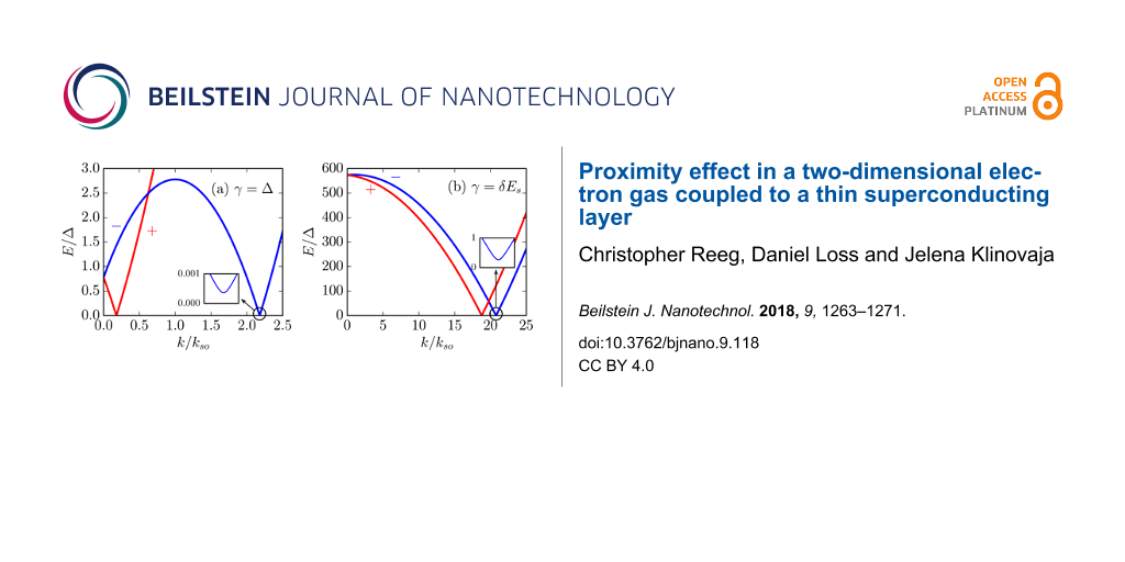
We plot the spectrum of the 2DEG (see Equation 19) in Figure 3. In the weak-coupling limit (Figure 3a), there is a rather small band shift but a negligible superconducting gap is opened in the 2DEG. In the strong-coupling limit (Figure 3b), we show that while a larger gap is induced, the band shift is very large.
![[2190-4286-9-118-3]](/bjnano/content/figures/2190-4286-9-118-3.png?scale=2.0&max-width=1024&background=FFFFFF)
Figure 3: Spectrum of a 2DEG coupled to a thin superconducting layer (see Equation 19) for (a) γ = Δ (corresponding to Γ = 0.9996 and δμ = 0.78Δ) and (b) γ = δEs (corresponding to Γ = 0.735 and δμ = 780Δ). When tunneling is weak (as in panel a), the band shift is rather small but the induced gap is negligible. If tunneling is strong enough to open a sizable gap (as in panel b), the band shift is very large (note that the band shift is given by E±(0) ~ Γδμ rather than δμ). In both plots, Eso = 2Δ, δEs = 1000Δ, μ2D = 0, kFd/π = 48.75, and kFz2D = 0.3. Here kso = mα is the spin–orbit momentum. Note that although, in the insets, we show only the induced gap on the "−"-subband, there is an equally large gap induced on the "+"-subband.
Figure 3: Spectrum of a 2DEG coupled to a thin superconducting layer (see Equation 19) for (a) γ = Δ (corresponding to Γ...
Topological transition
We now add a Zeeman splitting ΔZ to the Hamiltonian of the 2DEG such that
![[2190-4286-9-118-i23]](/bjnano/content/inline/2190-4286-9-118-i23.svg?max-width=590&scale=1.18182)
Such a Zeeman splitting can arise due to the application of an out-of-plane magnetic field [4,5] (though orbital effects are not incorporated here) or due to the proximity of a magnetic insulator [8]. Also, it is possible to apply an in-plane magnetic field (to avoid unwanted orbital effects) to reach the topological phase if the 2DEG has a finite Dresselhaus SOI, as shown in [9]. An in-plane magnetic field in the presence of only Rashba SOI is not sufficient to reach the topological phase because it does not open a gap in the Rashba spectrum. The spectrum in the presence of the Zeeman splitting, which again is determined by poles in the retarded Green’s function ![[Graphic 41]](/bjnano/content/inline/2190-4286-9-118-i68.svg?max-width=637&scale=1.18182) , is given by
, is given by
![[2190-4286-9-118-i24]](/bjnano/content/inline/2190-4286-9-118-i24.svg?max-width=590&scale=1.18182)
where we have used Eg = Δ(1 − Γ) as in Equation 20. Therefore, we find a gap-closing topological transition at k = 0 for the critical Zeeman splitting
![[2190-4286-9-118-i25]](/bjnano/content/inline/2190-4286-9-118-i25.svg?max-width=590&scale=1.18182)
In the case of a very large band shift, ![[Graphic 42]](/bjnano/content/inline/2190-4286-9-118-i69.svg?max-width=637&scale=1.18182) and
and ![[Graphic 43]](/bjnano/content/inline/2190-4286-9-118-i70.svg?max-width=637&scale=1.18182) , the topological transition is given by
, the topological transition is given by ![[Graphic 44]](/bjnano/content/inline/2190-4286-9-118-i71.svg?max-width=637&scale=1.18182) [note that Γ drops out of Equation 25 in this limit].
[note that Γ drops out of Equation 25 in this limit].
We now provide an estimate of the Zeeman splitting at which we expect the k = 0 gap-closing transition to occur experimentally in an Al/InAs 2DEG heterostructure. Given the thickness of the superconducting Al layer of d = 10 nm [44], we estimate a level spacing of δEs = ![[Graphic 45]](/bjnano/content/inline/2190-4286-9-118-i72.svg?max-width=637&scale=1.18182) = 413 meV (taking vF = 2 × 10⁶ m/s). Therefore, if a sizable gap is induced in the 2DEG, as observed experimentally, typical values for the band shift are of the same order of magnitude as the level spacing, Γδμ ~ 400 meV. Then, provided that the chemical potential cannot be controlled over such a large scale by external gates, the critical Zeeman splitting needed to reach the topological phase is
= 413 meV (taking vF = 2 × 10⁶ m/s). Therefore, if a sizable gap is induced in the 2DEG, as observed experimentally, typical values for the band shift are of the same order of magnitude as the level spacing, Γδμ ~ 400 meV. Then, provided that the chemical potential cannot be controlled over such a large scale by external gates, the critical Zeeman splitting needed to reach the topological phase is ![[Graphic 46]](/bjnano/content/inline/2190-4286-9-118-i73.svg?max-width=637&scale=1.18182) = δμ ~ 400 meV. Such a large Zeeman splitting cannot be achieved in the 2DEG without destroying superconductivity in the thin layer. We also note the possibility that, by coincidence, the band shift vanishes (or becomes small); from Equation 18, we see that δμ = 0 if kFd = cot−1(1/kFz2D) + nπ (for
= δμ ~ 400 meV. Such a large Zeeman splitting cannot be achieved in the 2DEG without destroying superconductivity in the thin layer. We also note the possibility that, by coincidence, the band shift vanishes (or becomes small); from Equation 18, we see that δμ = 0 if kFd = cot−1(1/kFz2D) + nπ (for ![[Graphic 47]](/bjnano/content/inline/2190-4286-9-118-i74.svg?max-width=637&scale=1.18182) ). In this special case, which requires the thickness of the superconducting layer to be finely tuned on the scale of its Fermi wavelength, there is no band shift to prevent one from tuning into a topological phase. However, for most devices, the large band shift makes it very challenging to realize a topological phase.
). In this special case, which requires the thickness of the superconducting layer to be finely tuned on the scale of its Fermi wavelength, there is no band shift to prevent one from tuning into a topological phase. However, for most devices, the large band shift makes it very challenging to realize a topological phase.
Increasing thickness of superconducting layer
The self-energy appearing most frequently in the literature to describe proximitized nanowires and 2DEGs [55-60], which also has been used often in interpreting experimental results [40,42], is that induced by a bulk superconductor,
![[2190-4286-9-118-i26]](/bjnano/content/inline/2190-4286-9-118-i26.svg?max-width=590&scale=1.18182)
Equation 26 can be obtained by setting z2D = d/2 and taking the limit d→∞ in Equation 15 (or, as it is usually done, by substituting the bulk Green’s function in Equation 13 when evaluating the self-energy in Equation 10). Hence, this self-energy describes a 2DEG embedded within a bulk superconductor, as shown in Figure 4a. To describe the case where a 2DEG is placed at the surface of a bulk superconductor (as shown in Figure 4b), the limit d→∞ should be taken in Equation 15 while keeping z2D finite (or, equivalently, substituting the Green’s function of a semi-infinite (SI) superconductor when evaluating the self-energy in Equation 10). For this case, we obtain
![[2190-4286-9-118-i27]](/bjnano/content/inline/2190-4286-9-118-i27.svg?max-width=590&scale=1.18182)
The most notable difference is the presence of a nonzero band shift in the semi-infinite case. However, this band shift is significantly reduced compared to the case of a thin superconducting layer, as it saturates to E±(0) ~ ΓSIδμSI ~ Δ in the limit ![[Graphic 48]](/bjnano/content/inline/2190-4286-9-118-i75.svg?max-width=637&scale=1.18182) .
.
![[2190-4286-9-118-4]](/bjnano/content/figures/2190-4286-9-118-4.png?scale=2.0&max-width=1024&background=FFFFFF)
Figure 4: (a) Evaluating the self-energy with the Green’s function of a bulk superconductor (see Equation 26) corresponds to a 2DEG embedded within an infinitely large superconductor. (b) Evaluating the self-energy with the Green’s function of a semi-infinite superconductor (see Equation 27) corresponds to a 2DEG placed on the surface of an infinitely large superconductor.
Figure 4: (a) Evaluating the self-energy with the Green’s function of a bulk superconductor (see Equation 26) correspond...
Although it may seem that a topological phase can be much more easily realized by simply increasing the thickness of the superconducting layer in order to reduce the band shift induced on the 2DEG, this is not the case. Crucially, both the bulk and the semi-infinite self-energies give the ratio γ/Δ as the relevant parameter determining whether the system is in the weak-coupling [![[Graphic 49]](/bjnano/content/inline/2190-4286-9-118-i76.svg?max-width=637&scale=1.18182) , or equivalently
, or equivalently ![[Graphic 50]](/bjnano/content/inline/2190-4286-9-118-i77.svg?max-width=637&scale=1.18182) ] or strong-coupling [(1 − Γ) ~ 1, or equivalently Eg ~ Δ] limit. This is in stark contrast to the limit of a thin superconducting layer, where a tunneling energy
] or strong-coupling [(1 − Γ) ~ 1, or equivalently Eg ~ Δ] limit. This is in stark contrast to the limit of a thin superconducting layer, where a tunneling energy ![[Graphic 51]](/bjnano/content/inline/2190-4286-9-118-i78.svg?max-width=637&scale=1.18182) is required to open a gap Eg ~ Δ in the 2DEG. Therefore, because the tunneling energy γ is a property of the interface and should not be expected to change as the thickness of the superconducting layer is increased, this energy is fixed to γ ~ δEs provided that the interface is transparent enough to induce a gap in the thin-layer limit (as seen in the experiments). If the thickness of the superconductor is increased, such that
is required to open a gap Eg ~ Δ in the 2DEG. Therefore, because the tunneling energy γ is a property of the interface and should not be expected to change as the thickness of the superconducting layer is increased, this energy is fixed to γ ~ δEs provided that the interface is transparent enough to induce a gap in the thin-layer limit (as seen in the experiments). If the thickness of the superconductor is increased, such that ![[Graphic 52]](/bjnano/content/inline/2190-4286-9-118-i79.svg?max-width=637&scale=1.18182) , the system will be deep within the strong-coupling limit; from Equation 26 and Equation 27, we find
, the system will be deep within the strong-coupling limit; from Equation 26 and Equation 27, we find ![[Graphic 53]](/bjnano/content/inline/2190-4286-9-118-i80.svg?max-width=637&scale=1.18182) . The critical Zeeman splitting needed to induce a topological phase (see Equation 25) is therefore given by
. The critical Zeeman splitting needed to induce a topological phase (see Equation 25) is therefore given by ![[Graphic 54]](/bjnano/content/inline/2190-4286-9-118-i81.svg?max-width=637&scale=1.18182) ~ Δ/Γ ~ γ ~ 400 meV. We note that in the case of a thin superconducting layer, the topological transition is pushed to large Zeeman splitting by very large δμ, which could possibly be compensated for if the chemical potential μ2D has a large range of tunability. In the case of a bulk system, the topological transition is pushed to large Zeeman splitting by very small Γ, which cannot be affected by tuning μ2D. Hence, even if the thickness d of the superconducting layer is made infinite, the topological phase transition is determined by the interfacial tunneling energy. In order to induce a topological phase more reliably, a much weaker coupling between a 2DEG and a bulk superconductor (such that γ ≤ Δ) should be sought. We also note that this result applies to the 1D model considered in [48] as well.)
~ Δ/Γ ~ γ ~ 400 meV. We note that in the case of a thin superconducting layer, the topological transition is pushed to large Zeeman splitting by very large δμ, which could possibly be compensated for if the chemical potential μ2D has a large range of tunability. In the case of a bulk system, the topological transition is pushed to large Zeeman splitting by very small Γ, which cannot be affected by tuning μ2D. Hence, even if the thickness d of the superconducting layer is made infinite, the topological phase transition is determined by the interfacial tunneling energy. In order to induce a topological phase more reliably, a much weaker coupling between a 2DEG and a bulk superconductor (such that γ ≤ Δ) should be sought. We also note that this result applies to the 1D model considered in [48] as well.)
Conclusion
We have studied the proximity effect in a two-dimensional electron gas (2DEG) strongly coupled to a thin superconducting layer, showing that the detrimental band shift shown in [48,49] to dominate the proximity effect in wires is also crucial in 2DEGs. In order to induce a sizable gap in the 2DEG, the tunneling energy scale must overcome the large level spacing within the superconductor. However, introducing such a large energy scale to the semiconductor induces a large band shift that makes it challenging to realize a topological phase. This challenge cannot be alleviated by simply increasing the thickness of the superconducting layer but requires a significant weakening of the proximity coupling afforded by the epitaxial interface.
References
-
Kitaev, A. Y. Phys.-Usp. 2001, 44, 131. doi:10.1070/1063-7869/44/10S/S29
Return to citation in text: [1] -
Nayak, C.; Simon, S. H.; Stern, A.; Freedman, M.; Das Sarma, S. Rev. Mod. Phys. 2008, 80, 1083. doi:10.1103/RevModPhys.80.1083
Return to citation in text: [1] -
Alicea, J. Rep. Prog. Phys. 2012, 75, 076501. doi:10.1088/0034-4885/75/7/076501
Return to citation in text: [1] -
Sato, M.; Fujimoto, S. Phys. Rev. B 2009, 79, 094504. doi:10.1103/PhysRevB.79.094504
Return to citation in text: [1] [2] -
Sato, M.; Takahashi, Y.; Fujimoto, S. Phys. Rev. Lett. 2009, 103, 020401. doi:10.1103/PhysRevLett.103.020401
Return to citation in text: [1] [2] -
Lutchyn, R. M.; Sau, J. D.; Das Sarma, S. Phys. Rev. Lett. 2010, 105, 077001. doi:10.1103/PhysRevLett.105.077001
Return to citation in text: [1] -
Oreg, Y.; Refael, G.; von Oppen, F. Phys. Rev. Lett. 2010, 105, 177002. doi:10.1103/PhysRevLett.105.177002
Return to citation in text: [1] -
Sau, J. D.; Lutchyn, R. M.; Tewari, S.; Das Sarma, S. Phys. Rev. Lett. 2010, 104, 040502. doi:10.1103/PhysRevLett.104.040502
Return to citation in text: [1] [2] -
Alicea, J. Phys. Rev. B 2010, 81, 125318. doi:10.1103/PhysRevB.81.125318
Return to citation in text: [1] [2] -
Chevallier, D.; Sticlet, D.; Simon, P.; Bena, C. Phys. Rev. B 2012, 85, 235307. doi:10.1103/PhysRevB.85.235307
Return to citation in text: [1] -
Halperin, B. I.; Oreg, Y.; Stern, A.; Refael, G.; Alicea, J.; von Oppen, F. Phys. Rev. B 2012, 85, 144501. doi:10.1103/PhysRevB.85.144501
Return to citation in text: [1] -
Sticlet, D.; Bena, C.; Simon, P. Phys. Rev. Lett. 2012, 108, 096802. doi:10.1103/PhysRevLett.108.096802
Return to citation in text: [1] -
Klinovaja, J.; Stano, P.; Loss, D. Phys. Rev. Lett. 2012, 109, 236801. doi:10.1103/PhysRevLett.109.236801
Return to citation in text: [1] -
Klinovaja, J.; Gangadharaiah, S.; Loss, D. Phys. Rev. Lett. 2012, 108, 196804. doi:10.1103/PhysRevLett.108.196804
Return to citation in text: [1] -
Prada, E.; San-Jose, P.; Aguado, R. Phys. Rev. B 2012, 86, 180503. doi:10.1103/PhysRevB.86.180503
Return to citation in text: [1] -
Domínguez, F.; Hassler, F.; Platero, G. Phys. Rev. B 2012, 86, 140503. doi:10.1103/PhysRevB.86.140503
Return to citation in text: [1] -
Klinovaja, J.; Loss, D. Phys. Rev. X 2013, 3, 011008. doi:10.1103/PhysRevX.3.011008
Return to citation in text: [1] -
DeGottardi, W.; Thakurathi, M.; Vishveshwara, S.; Sen, D. Phys. Rev. B 2013, 88, 165111. doi:10.1103/PhysRevB.88.165111
Return to citation in text: [1] -
Maier, F.; Klinovaja, J.; Loss, D. Phys. Rev. B 2014, 90, 195421. doi:10.1103/PhysRevB.90.195421
Return to citation in text: [1] -
Vernek, E.; Penteado, P. H.; Seridonio, A. C.; Egues, J. C. Phys. Rev. B 2014, 89, 165314. doi:10.1103/PhysRevB.89.165314
Return to citation in text: [1] -
Weithofer, L.; Recher, P.; Schmidt, T. L. Phys. Rev. B 2014, 90, 205416. doi:10.1103/PhysRevB.90.205416
Return to citation in text: [1] -
Thakurathi, M.; Deb, O.; Sen, D. J. Phys.: Condens. Matter 2015, 27, 275702. doi:10.1088/0953-8984/27/27/275702
Return to citation in text: [1] -
Dmytruk, O.; Trif, M.; Simon, P. Phys. Rev. B 2015, 92, 245432. doi:10.1103/PhysRevB.92.245432
Return to citation in text: [1] -
Nadj-Perge, S.; Drozdov, I. K.; Li, J.; Chen, H.; Jeon, S.; Seo, J.; MacDonald, A. H.; Bernevig, B. A.; Yazdani, A. Science 2014, 346, 602. doi:10.1126/science.1259327
Return to citation in text: [1] -
Ruby, M.; Pientka, F.; Peng, Y.; von Oppen, F.; Heinrich, B. W.; Franke, K. J. Phys. Rev. Lett. 2015, 115, 197204. doi:10.1103/PhysRevLett.115.197204
Return to citation in text: [1] -
Pawlak, R.; Kisiel, M.; Klinovaja, J.; Meier, T.; Kawai, S.; Glatzel, T.; Loss, D.; Meyer, E. npj Quantum Inf. 2016, 2, 16035. doi:10.1038/npjqi.2016.35
Return to citation in text: [1] -
Klinovaja, J.; Stano, P.; Yazdani, A.; Loss, D. Phys. Rev. Lett. 2013, 111, 186805. doi:10.1103/PhysRevLett.111.186805
Return to citation in text: [1] -
Vazifeh, M. M.; Franz, M. Phys. Rev. Lett. 2013, 111, 206802. doi:10.1103/PhysRevLett.111.206802
Return to citation in text: [1] -
Braunecker, B.; Simon, P. Phys. Rev. Lett. 2013, 111, 147202. doi:10.1103/PhysRevLett.111.147202
Return to citation in text: [1] -
Nadj-Perge, S.; Drozdov, I. K.; Bernevig, B. A.; Yazdani, A. Phys. Rev. B 2013, 88, 020407. doi:10.1103/PhysRevB.88.020407
Return to citation in text: [1] -
Pientka, F.; Glazman, L. I.; von Oppen, F. Phys. Rev. B 2013, 88, 155420. doi:10.1103/PhysRevB.88.155420
Return to citation in text: [1] -
Awoga, O. A.; Björnson, K.; Black-Schaffer, A. M. Phys. Rev. B 2017, 95, 184511. doi:10.1103/PhysRevB.95.184511
Return to citation in text: [1] -
Mourik, V.; Zuo, K.; Frolov, S. M.; Plissard, S. R.; Bakkers, E. P. A. M.; Kouwenhoven, L. P. Science 2012, 336, 1003. doi:10.1126/science.1222360
Return to citation in text: [1] -
Deng, M. T.; Yu, C. L.; Huang, G. Y.; Larsson, M.; Caroff, P.; Xu, H. Q. Nano Lett. 2012, 12, 6414. doi:10.1021/nl303758w
Return to citation in text: [1] -
Das, A.; Ronen, Y.; Most, Y.; Oreg, Y.; Heiblum, M.; Shtrikman, H. Nat. Phys. 2012, 8, 887. doi:10.1038/nphys2479
Return to citation in text: [1] -
Churchill, H. O. H.; Fatemi, V.; Grove-Rasmussen, K.; Deng, M. T.; Caroff, P.; Xu, H. Q.; Marcus, C. M. Phys. Rev. B 2013, 87, 241401. doi:10.1103/PhysRevB.87.241401
Return to citation in text: [1] -
Finck, A. D. K.; Van Harlingen, D. J.; Mohseni, P. K.; Jung, K.; Li, X. Phys. Rev. Lett. 2013, 110, 126406. doi:10.1103/PhysRevLett.110.126406
Return to citation in text: [1] -
Chang, W.; Albrecht, S. M.; Jespersen, T. S.; Kuemmeth, F.; Krogstrup, P.; Nygård, J.; Marcus, C. M. Nat. Nanotechnol. 2015, 10, 232. doi:10.1038/nnano.2014.306
Return to citation in text: [1] -
Albrecht, S. M.; Higginbotham, A. P.; Madsen, M.; Kuemmeth, F.; Jespersen, T. S.; Nygård, J.; Krogstrup, P.; Marcus, C. M. Nature 2016, 531, 206–209. doi:10.1038/nature17162
Return to citation in text: [1] -
Deng, M. T.; Vaitiekėnas, S.; Hansen, E. B.; Danon, J.; Leijnse, M.; Flensberg, K.; Nygård, J.; Krogstrup, P.; Marcus, C. M. Science 2016, 354, 1557. doi:10.1126/science.aaf3961
Return to citation in text: [1] [2] -
Gazibegovic, S.; Car, D.; Zhang, H.; Balk, S. C.; Logan, J. A.; de Moor, M. W. A.; Cassidy, M. C.; Schmits, R.; Xu, D.; Wang, G.; Krogstrup, P.; Op het Veld, R. L. M.; Zuo, K.; Vos, Y.; Shen, J.; Bouman, D.; Shojaei, B.; Pennachio, D.; Lee, J. S.; van Veldhoven, P. J.; Koelling, S.; Verheijen, M. A.; Kouwenhoven, L. P.; Palmstrøm, C. J.; Bakkers, E. P. A. M. Nature 2017, 548, 434. doi:10.1038/nature23468
Return to citation in text: [1] -
Zhang, H.; Liu, C.-X.; Gazibegovic, S.; Xu, D.; Logan, J. A.; Wang, G.; van Loo, N.; Bommer, J. D. S.; de Moor, M. W. A.; Car, D.; het Veld, R. L. M. O.; van Veldhoven, P. J.; Koelling, S.; Verheijen, M. A.; Pendharkar, M.; Pennachio, D. J.; Shojaei, B.; Lee, J. S.; Palmstrom, C. J.; Bakkers, E. P. A. M.; Das Sarma, S.; Kouwenhoven, L. P. arXiv 2017, No. 1710.10701.
Return to citation in text: [1] [2] -
Kjaergaard, M.; Nichele, F.; Suominen, H. J.; Nowak, M. P.; Wimmer, M.; Akhmerov, A. R.; Folk, J. A.; Flensberg, K.; Shabani, J.; Palmstrøm, C. J.; Marcus, C. M. Nat. Commun. 2016, 7, 12841. doi:10.1038/ncomms12841
Return to citation in text: [1] -
Shabani, J.; Kjaergaard, M.; Suominen, H. J.; Kim, Y.; Nichele, F.; Pakrouski, K.; Stankevic, T.; Lutchyn, R. M.; Krogstrup, P.; Feidenhans’l, R.; Kraemer, S.; Nayak, C.; Troyer, M.; Marcus, C. M.; Palmstrøm, C. J. Phys. Rev. B 2016, 93, 155402. doi:10.1103/PhysRevB.93.155402
Return to citation in text: [1] [2] -
Kjaergaard, M.; Suominen, H. J.; Nowak, M. P.; Akhmerov, A. R.; Shabani, J.; Palmstrøm, C. J.; Nichele, F.; Marcus, C. M. Phys. Rev. Appl. 2017, 7, 034029. doi:10.1103/PhysRevApplied.7.034029
Return to citation in text: [1] -
Suominen, H. J.; Kjaergaard, M.; Hamilton, A. R.; Shabani, J.; Palmstrøm, C. J.; Marcus, C. M.; Nichele, F. Phys. Rev. Lett. 2017, 119, 176805. doi:10.1103/PhysRevLett.119.176805
Return to citation in text: [1] -
Nichele, F.; Drachmann, A. C. C.; Whiticar, A. M.; O’Farrell, E. C. T.; Suominen, H. J.; Fornieri, A.; Wang, T.; Gardner, G. C.; Thomas, C.; Hatke, A. T.; Krogstrup, P.; Manfra, M. J.; Flensberg, K.; Marcus, C. M. Phys. Rev. Lett. 2017, 119, 136803. doi:10.1103/PhysRevLett.119.136803
Return to citation in text: [1] -
Reeg, C.; Loss, D.; Klinovaja, J. Phys. Rev. B 2017, 96, 125426. doi:10.1103/PhysRevB.96.125426
Return to citation in text: [1] [2] [3] [4] [5] [6] [7] [8] -
Reeg, C.; Loss, D.; Klinovaja, J. arXiv 2018, No. 1801.06509.
Return to citation in text: [1] [2] [3] -
Volkov, A. F.; Magnée, P. H. C.; van Wees, B. J.; Klapwijk, T. M. Physica C 1995, 242, 261. doi:10.1016/0921-4534(94)02429-4
Return to citation in text: [1] -
Fagas, G.; Tkachov, G.; Pfund, A.; Richter, K. Phys. Rev. B 2005, 71, 224510. doi:10.1103/PhysRevB.71.224510
Return to citation in text: [1] -
Tkachov, G. Physica C 2005, 417, 127. doi:10.1016/j.physc.2004.10.015
Return to citation in text: [1] -
Reeg, C. R.; Maslov, D. L. Phys. Rev. B 2016, 94, 020501. doi:10.1103/PhysRevB.94.020501
Return to citation in text: [1] -
Reeg, C.; Klinovaja, J.; Loss, D. Phys. Rev. B 2017, 96, 081301. doi:10.1103/PhysRevB.96.081301
Return to citation in text: [1] -
Sau, J. D.; Lutchyn, R. M.; Tewari, S.; Das Sarma, S. Phys. Rev. B 2010, 82, 094522. doi:10.1103/PhysRevB.82.094522
Return to citation in text: [1] -
Potter, A. C.; Lee, P. A. Phys. Rev. B 2011, 83, 184520. doi:10.1103/PhysRevB.83.184520
Return to citation in text: [1] -
Kopnin, N. B.; Melnikov, A. S. Phys. Rev. B 2011, 84, 064524. doi:10.1103/PhysRevB.84.064524
Return to citation in text: [1] -
Zyuzin, A. A.; Rainis, D.; Klinovaja, J.; Loss, D. Phys. Rev. Lett. 2013, 111, 056802. doi:10.1103/PhysRevLett.111.056802
Return to citation in text: [1] -
van Heck, B.; Lutchyn, R. M.; Glazman, L. I. Phys. Rev. B 2016, 93, 235431. doi:10.1103/PhysRevB.93.235431
Return to citation in text: [1] -
Reeg, C.; Maslov, D. L. Phys. Rev. B 2017, 95, 205439. doi:10.1103/PhysRevB.95.205439
Return to citation in text: [1]
| 55. | Sau, J. D.; Lutchyn, R. M.; Tewari, S.; Das Sarma, S. Phys. Rev. B 2010, 82, 094522. doi:10.1103/PhysRevB.82.094522 |
| 56. | Potter, A. C.; Lee, P. A. Phys. Rev. B 2011, 83, 184520. doi:10.1103/PhysRevB.83.184520 |
| 57. | Kopnin, N. B.; Melnikov, A. S. Phys. Rev. B 2011, 84, 064524. doi:10.1103/PhysRevB.84.064524 |
| 58. | Zyuzin, A. A.; Rainis, D.; Klinovaja, J.; Loss, D. Phys. Rev. Lett. 2013, 111, 056802. doi:10.1103/PhysRevLett.111.056802 |
| 59. | van Heck, B.; Lutchyn, R. M.; Glazman, L. I. Phys. Rev. B 2016, 93, 235431. doi:10.1103/PhysRevB.93.235431 |
| 60. | Reeg, C.; Maslov, D. L. Phys. Rev. B 2017, 95, 205439. doi:10.1103/PhysRevB.95.205439 |
| 44. | Shabani, J.; Kjaergaard, M.; Suominen, H. J.; Kim, Y.; Nichele, F.; Pakrouski, K.; Stankevic, T.; Lutchyn, R. M.; Krogstrup, P.; Feidenhans’l, R.; Kraemer, S.; Nayak, C.; Troyer, M.; Marcus, C. M.; Palmstrøm, C. J. Phys. Rev. B 2016, 93, 155402. doi:10.1103/PhysRevB.93.155402 |
| 1. | Kitaev, A. Y. Phys.-Usp. 2001, 44, 131. doi:10.1070/1063-7869/44/10S/S29 |
| 2. | Nayak, C.; Simon, S. H.; Stern, A.; Freedman, M.; Das Sarma, S. Rev. Mod. Phys. 2008, 80, 1083. doi:10.1103/RevModPhys.80.1083 |
| 3. | Alicea, J. Rep. Prog. Phys. 2012, 75, 076501. doi:10.1088/0034-4885/75/7/076501 |
| 38. | Chang, W.; Albrecht, S. M.; Jespersen, T. S.; Kuemmeth, F.; Krogstrup, P.; Nygård, J.; Marcus, C. M. Nat. Nanotechnol. 2015, 10, 232. doi:10.1038/nnano.2014.306 |
| 39. | Albrecht, S. M.; Higginbotham, A. P.; Madsen, M.; Kuemmeth, F.; Jespersen, T. S.; Nygård, J.; Krogstrup, P.; Marcus, C. M. Nature 2016, 531, 206–209. doi:10.1038/nature17162 |
| 40. | Deng, M. T.; Vaitiekėnas, S.; Hansen, E. B.; Danon, J.; Leijnse, M.; Flensberg, K.; Nygård, J.; Krogstrup, P.; Marcus, C. M. Science 2016, 354, 1557. doi:10.1126/science.aaf3961 |
| 41. | Gazibegovic, S.; Car, D.; Zhang, H.; Balk, S. C.; Logan, J. A.; de Moor, M. W. A.; Cassidy, M. C.; Schmits, R.; Xu, D.; Wang, G.; Krogstrup, P.; Op het Veld, R. L. M.; Zuo, K.; Vos, Y.; Shen, J.; Bouman, D.; Shojaei, B.; Pennachio, D.; Lee, J. S.; van Veldhoven, P. J.; Koelling, S.; Verheijen, M. A.; Kouwenhoven, L. P.; Palmstrøm, C. J.; Bakkers, E. P. A. M. Nature 2017, 548, 434. doi:10.1038/nature23468 |
| 42. | Zhang, H.; Liu, C.-X.; Gazibegovic, S.; Xu, D.; Logan, J. A.; Wang, G.; van Loo, N.; Bommer, J. D. S.; de Moor, M. W. A.; Car, D.; het Veld, R. L. M. O.; van Veldhoven, P. J.; Koelling, S.; Verheijen, M. A.; Pendharkar, M.; Pennachio, D. J.; Shojaei, B.; Lee, J. S.; Palmstrom, C. J.; Bakkers, E. P. A. M.; Das Sarma, S.; Kouwenhoven, L. P. arXiv 2017, No. 1710.10701. |
| 4. | Sato, M.; Fujimoto, S. Phys. Rev. B 2009, 79, 094504. doi:10.1103/PhysRevB.79.094504 |
| 5. | Sato, M.; Takahashi, Y.; Fujimoto, S. Phys. Rev. Lett. 2009, 103, 020401. doi:10.1103/PhysRevLett.103.020401 |
| 33. | Mourik, V.; Zuo, K.; Frolov, S. M.; Plissard, S. R.; Bakkers, E. P. A. M.; Kouwenhoven, L. P. Science 2012, 336, 1003. doi:10.1126/science.1222360 |
| 34. | Deng, M. T.; Yu, C. L.; Huang, G. Y.; Larsson, M.; Caroff, P.; Xu, H. Q. Nano Lett. 2012, 12, 6414. doi:10.1021/nl303758w |
| 35. | Das, A.; Ronen, Y.; Most, Y.; Oreg, Y.; Heiblum, M.; Shtrikman, H. Nat. Phys. 2012, 8, 887. doi:10.1038/nphys2479 |
| 36. | Churchill, H. O. H.; Fatemi, V.; Grove-Rasmussen, K.; Deng, M. T.; Caroff, P.; Xu, H. Q.; Marcus, C. M. Phys. Rev. B 2013, 87, 241401. doi:10.1103/PhysRevB.87.241401 |
| 37. | Finck, A. D. K.; Van Harlingen, D. J.; Mohseni, P. K.; Jung, K.; Li, X. Phys. Rev. Lett. 2013, 110, 126406. doi:10.1103/PhysRevLett.110.126406 |
| 8. | Sau, J. D.; Lutchyn, R. M.; Tewari, S.; Das Sarma, S. Phys. Rev. Lett. 2010, 104, 040502. doi:10.1103/PhysRevLett.104.040502 |
| 24. | Nadj-Perge, S.; Drozdov, I. K.; Li, J.; Chen, H.; Jeon, S.; Seo, J.; MacDonald, A. H.; Bernevig, B. A.; Yazdani, A. Science 2014, 346, 602. doi:10.1126/science.1259327 |
| 25. | Ruby, M.; Pientka, F.; Peng, Y.; von Oppen, F.; Heinrich, B. W.; Franke, K. J. Phys. Rev. Lett. 2015, 115, 197204. doi:10.1103/PhysRevLett.115.197204 |
| 26. | Pawlak, R.; Kisiel, M.; Klinovaja, J.; Meier, T.; Kawai, S.; Glatzel, T.; Loss, D.; Meyer, E. npj Quantum Inf. 2016, 2, 16035. doi:10.1038/npjqi.2016.35 |
| 27. | Klinovaja, J.; Stano, P.; Yazdani, A.; Loss, D. Phys. Rev. Lett. 2013, 111, 186805. doi:10.1103/PhysRevLett.111.186805 |
| 28. | Vazifeh, M. M.; Franz, M. Phys. Rev. Lett. 2013, 111, 206802. doi:10.1103/PhysRevLett.111.206802 |
| 29. | Braunecker, B.; Simon, P. Phys. Rev. Lett. 2013, 111, 147202. doi:10.1103/PhysRevLett.111.147202 |
| 30. | Nadj-Perge, S.; Drozdov, I. K.; Bernevig, B. A.; Yazdani, A. Phys. Rev. B 2013, 88, 020407. doi:10.1103/PhysRevB.88.020407 |
| 31. | Pientka, F.; Glazman, L. I.; von Oppen, F. Phys. Rev. B 2013, 88, 155420. doi:10.1103/PhysRevB.88.155420 |
| 32. | Awoga, O. A.; Björnson, K.; Black-Schaffer, A. M. Phys. Rev. B 2017, 95, 184511. doi:10.1103/PhysRevB.95.184511 |
| 48. | Reeg, C.; Loss, D.; Klinovaja, J. Phys. Rev. B 2017, 96, 125426. doi:10.1103/PhysRevB.96.125426 |
| 54. | Reeg, C.; Klinovaja, J.; Loss, D. Phys. Rev. B 2017, 96, 081301. doi:10.1103/PhysRevB.96.081301 |
| 4. | Sato, M.; Fujimoto, S. Phys. Rev. B 2009, 79, 094504. doi:10.1103/PhysRevB.79.094504 |
| 5. | Sato, M.; Takahashi, Y.; Fujimoto, S. Phys. Rev. Lett. 2009, 103, 020401. doi:10.1103/PhysRevLett.103.020401 |
| 6. | Lutchyn, R. M.; Sau, J. D.; Das Sarma, S. Phys. Rev. Lett. 2010, 105, 077001. doi:10.1103/PhysRevLett.105.077001 |
| 7. | Oreg, Y.; Refael, G.; von Oppen, F. Phys. Rev. Lett. 2010, 105, 177002. doi:10.1103/PhysRevLett.105.177002 |
| 8. | Sau, J. D.; Lutchyn, R. M.; Tewari, S.; Das Sarma, S. Phys. Rev. Lett. 2010, 104, 040502. doi:10.1103/PhysRevLett.104.040502 |
| 9. | Alicea, J. Phys. Rev. B 2010, 81, 125318. doi:10.1103/PhysRevB.81.125318 |
| 10. | Chevallier, D.; Sticlet, D.; Simon, P.; Bena, C. Phys. Rev. B 2012, 85, 235307. doi:10.1103/PhysRevB.85.235307 |
| 11. | Halperin, B. I.; Oreg, Y.; Stern, A.; Refael, G.; Alicea, J.; von Oppen, F. Phys. Rev. B 2012, 85, 144501. doi:10.1103/PhysRevB.85.144501 |
| 12. | Sticlet, D.; Bena, C.; Simon, P. Phys. Rev. Lett. 2012, 108, 096802. doi:10.1103/PhysRevLett.108.096802 |
| 13. | Klinovaja, J.; Stano, P.; Loss, D. Phys. Rev. Lett. 2012, 109, 236801. doi:10.1103/PhysRevLett.109.236801 |
| 14. | Klinovaja, J.; Gangadharaiah, S.; Loss, D. Phys. Rev. Lett. 2012, 108, 196804. doi:10.1103/PhysRevLett.108.196804 |
| 15. | Prada, E.; San-Jose, P.; Aguado, R. Phys. Rev. B 2012, 86, 180503. doi:10.1103/PhysRevB.86.180503 |
| 16. | Domínguez, F.; Hassler, F.; Platero, G. Phys. Rev. B 2012, 86, 140503. doi:10.1103/PhysRevB.86.140503 |
| 17. | Klinovaja, J.; Loss, D. Phys. Rev. X 2013, 3, 011008. doi:10.1103/PhysRevX.3.011008 |
| 18. | DeGottardi, W.; Thakurathi, M.; Vishveshwara, S.; Sen, D. Phys. Rev. B 2013, 88, 165111. doi:10.1103/PhysRevB.88.165111 |
| 19. | Maier, F.; Klinovaja, J.; Loss, D. Phys. Rev. B 2014, 90, 195421. doi:10.1103/PhysRevB.90.195421 |
| 20. | Vernek, E.; Penteado, P. H.; Seridonio, A. C.; Egues, J. C. Phys. Rev. B 2014, 89, 165314. doi:10.1103/PhysRevB.89.165314 |
| 21. | Weithofer, L.; Recher, P.; Schmidt, T. L. Phys. Rev. B 2014, 90, 205416. doi:10.1103/PhysRevB.90.205416 |
| 22. | Thakurathi, M.; Deb, O.; Sen, D. J. Phys.: Condens. Matter 2015, 27, 275702. doi:10.1088/0953-8984/27/27/275702 |
| 23. | Dmytruk, O.; Trif, M.; Simon, P. Phys. Rev. B 2015, 92, 245432. doi:10.1103/PhysRevB.92.245432 |
| 48. | Reeg, C.; Loss, D.; Klinovaja, J. Phys. Rev. B 2017, 96, 125426. doi:10.1103/PhysRevB.96.125426 |
| 48. | Reeg, C.; Loss, D.; Klinovaja, J. Phys. Rev. B 2017, 96, 125426. doi:10.1103/PhysRevB.96.125426 |
| 49. | Reeg, C.; Loss, D.; Klinovaja, J. arXiv 2018, No. 1801.06509. |
| 50. | Volkov, A. F.; Magnée, P. H. C.; van Wees, B. J.; Klapwijk, T. M. Physica C 1995, 242, 261. doi:10.1016/0921-4534(94)02429-4 |
| 51. | Fagas, G.; Tkachov, G.; Pfund, A.; Richter, K. Phys. Rev. B 2005, 71, 224510. doi:10.1103/PhysRevB.71.224510 |
| 52. | Tkachov, G. Physica C 2005, 417, 127. doi:10.1016/j.physc.2004.10.015 |
| 53. | Reeg, C. R.; Maslov, D. L. Phys. Rev. B 2016, 94, 020501. doi:10.1103/PhysRevB.94.020501 |
| 48. | Reeg, C.; Loss, D.; Klinovaja, J. Phys. Rev. B 2017, 96, 125426. doi:10.1103/PhysRevB.96.125426 |
| 49. | Reeg, C.; Loss, D.; Klinovaja, J. arXiv 2018, No. 1801.06509. |
| 48. | Reeg, C.; Loss, D.; Klinovaja, J. Phys. Rev. B 2017, 96, 125426. doi:10.1103/PhysRevB.96.125426 |
| 48. | Reeg, C.; Loss, D.; Klinovaja, J. Phys. Rev. B 2017, 96, 125426. doi:10.1103/PhysRevB.96.125426 |
| 40. | Deng, M. T.; Vaitiekėnas, S.; Hansen, E. B.; Danon, J.; Leijnse, M.; Flensberg, K.; Nygård, J.; Krogstrup, P.; Marcus, C. M. Science 2016, 354, 1557. doi:10.1126/science.aaf3961 |
| 42. | Zhang, H.; Liu, C.-X.; Gazibegovic, S.; Xu, D.; Logan, J. A.; Wang, G.; van Loo, N.; Bommer, J. D. S.; de Moor, M. W. A.; Car, D.; het Veld, R. L. M. O.; van Veldhoven, P. J.; Koelling, S.; Verheijen, M. A.; Pendharkar, M.; Pennachio, D. J.; Shojaei, B.; Lee, J. S.; Palmstrom, C. J.; Bakkers, E. P. A. M.; Das Sarma, S.; Kouwenhoven, L. P. arXiv 2017, No. 1710.10701. |
| 43. | Kjaergaard, M.; Nichele, F.; Suominen, H. J.; Nowak, M. P.; Wimmer, M.; Akhmerov, A. R.; Folk, J. A.; Flensberg, K.; Shabani, J.; Palmstrøm, C. J.; Marcus, C. M. Nat. Commun. 2016, 7, 12841. doi:10.1038/ncomms12841 |
| 44. | Shabani, J.; Kjaergaard, M.; Suominen, H. J.; Kim, Y.; Nichele, F.; Pakrouski, K.; Stankevic, T.; Lutchyn, R. M.; Krogstrup, P.; Feidenhans’l, R.; Kraemer, S.; Nayak, C.; Troyer, M.; Marcus, C. M.; Palmstrøm, C. J. Phys. Rev. B 2016, 93, 155402. doi:10.1103/PhysRevB.93.155402 |
| 45. | Kjaergaard, M.; Suominen, H. J.; Nowak, M. P.; Akhmerov, A. R.; Shabani, J.; Palmstrøm, C. J.; Nichele, F.; Marcus, C. M. Phys. Rev. Appl. 2017, 7, 034029. doi:10.1103/PhysRevApplied.7.034029 |
| 46. | Suominen, H. J.; Kjaergaard, M.; Hamilton, A. R.; Shabani, J.; Palmstrøm, C. J.; Marcus, C. M.; Nichele, F. Phys. Rev. Lett. 2017, 119, 176805. doi:10.1103/PhysRevLett.119.176805 |
| 47. | Nichele, F.; Drachmann, A. C. C.; Whiticar, A. M.; O’Farrell, E. C. T.; Suominen, H. J.; Fornieri, A.; Wang, T.; Gardner, G. C.; Thomas, C.; Hatke, A. T.; Krogstrup, P.; Manfra, M. J.; Flensberg, K.; Marcus, C. M. Phys. Rev. Lett. 2017, 119, 136803. doi:10.1103/PhysRevLett.119.136803 |
| 48. | Reeg, C.; Loss, D.; Klinovaja, J. Phys. Rev. B 2017, 96, 125426. doi:10.1103/PhysRevB.96.125426 |
| 48. | Reeg, C.; Loss, D.; Klinovaja, J. Phys. Rev. B 2017, 96, 125426. doi:10.1103/PhysRevB.96.125426 |
© 2018 Reeg et al.; licensee Beilstein-Institut.
This is an Open Access article under the terms of the Creative Commons Attribution License (http://creativecommons.org/licenses/by/4.0), which permits unrestricted use, distribution, and reproduction in any medium, provided the original work is properly cited.
The license is subject to the Beilstein Journal of Nanotechnology terms and conditions: (https://www.beilstein-journals.org/bjnano)