Abstract
The detection of single gas molecules is a highly challenging work because it requires sensors with an ultra-high level of sensitivity. By using density functional theory, here we demonstrate that the adsorption of a paramagnetic unpaired free radical gas (NO) on a monolayer of XS2 (X = Mo, W) can trigger the transition from semiconductor to half metal. More precisely, the single-layer XS2 (X = Mo, W) with NO adsorbed on it would behave like a metal in one spin channel while acting as a semiconductor in the other spin orientation. The half-metallicity is robust and independent of the NO concentration. In contrast, no half-metallic feature can be observed after the adsorption of other free radical gases such as NO2. The unique change in electronic properties after the adsorption of NO on transition-metal sulfides highlights an effective strategy to distinguish NO from other gas species by experimentally measuring spin-resolved transmission. Our results also suggest XS2 (X = Mo, W) nanosheets can act as promising nanoscale NO sensors.
Introduction
Nitrogen oxide (NOx) gases, one of the most common groups of air pollutants, are known as one culprit of acid rain and can cause serious health issues [1]. For a large-scale monitoring of NOx, it is highly essential to develop the techniques of toxic gas detection. Up to now, a number of three dimensional (3D) materials, such as nickel phthalocyanine (NiPc) [2], tungsten trioxide (WO3) [3], mesoporous silicate [4], composites of nanoflower-like CuxO and multilayer graphene (CuMGCs) [5] have been successfully synthesized as new types of room-temperature NO gas sensors.
Compared with 3D materials [6], two-dimensional (2D) materials (sheets with thickness of on atom) [7-15] such as graphene [8,16], phosphorene [9], siligraphene (SiC5) [10] and molybdenum disulfide (MoS2) [11,17] possess a high specific surface area and high electrical conductivity making them the ideal candidates for gas sensors. In particular, investigations of XS2-based (X = Mo, W) monolayer nanodevices demonstrate that they are ultra-sensitive to a number of molecules that are important in environmental studies [18-26]. More specifically, it has been suggested that MoS2 exhibits ultrahigh sensitivity to the adsorption of paramagnetic gases such as NO and NO2 [11]. Single-layer MoS2 has been confirmed to be a good candidate for fabricating field-effect transistor (FET) sensors for NO with high mobility at room temperature [17], and the detection offers a high sensitivity and rapid current response. However, the detailed mechanism regarding the interaction between the MoS2 surface and the gas molecules remains unclear. In addition to MoS2, 2D WS2 is expected to be a more promising material as gas sensor because of its higher thermal stability and wider temperature range of operation [18]. Synthesized FETs layered with WS2 are also reported as attractive electronic devices [27]. Besides, the corresponding binding position and energy of NO adsorbed on single-layer MoS2 [23] and WS2 [28] were analyzed from a theoretical point of view. Even though the gas-sensing properties involving NO and NO2 are well studied, few studies [29] have been carried out to explore the difference in spin-polarized gas-sensing between NO and other gas molecules.
A completely spin-polarized current flow can be achieved in a half-metallic material [30-33]. Half-metallic materials exhibit semiconducting behavior in one spin channel and metallic behavior in the opposite spin channel, which could be uses in spintronics. But the lack of suitable materials limits the development of spintronic applications. Doping semiconductors may be applied to achieve spin-polarized currents, but this requires a complicated process. Although many materials have been predicted in theory for this purpose, only few possess all necessary properties and many of them are unstable. Therefore, to explore more experimentally feasible and stable half-metallic materials is highly desirable.
In this paper, a density functional theory (DFT) study is carried out to show that monolayer XS2 (X = Mo, W) can selectively detect NO by exhibiting half-metallicity after physical adsorption of gas on the surface. For comparison, an investigation of NO2 adsorbed on single-layer XS2 (X = Mo, W) is also presented as both NO and NO2 are free radicals and can introduce magnetic moments to the gas/XS2 (X = Mo, W) system. The binding position and adsorption energy are analyzed in detail. In terms of the projected density of states (PDOS) and orbital contribution, our results offer a deep insight into the Fermi-level pinning mechanism. In addition, we expand the calculations to other 2D layered materials including GaS, GaSe, SnS, SnSe, WSe and Bi2Se3 (Figure S1, Supporting Information File 1). To the best of our knowledge, our work is the first to propose a NO sensor by detecting spin transmission, which may probe a new prospect for gas sensing.
Computational Methods
The spin-polarized calculations for NO, NO2, and NO, NO2 adsorbed on monolayer XS2 (X = Mo, W) are performed using DFT within generalized gradient approximation (GGA) of the Perdew–Burke–Ernzerhof (PBE) functional, as implemented in the Vienna ab initio simulation package (VASP) [34-36]. To study 2D systems under the periodic boundary conditions, a vacuum layer with a thickness of more than 20 Å was set to minimize artificial interactions between neighboring layers. A dispersion correction of total energy (DFT-D3 method) [37] is used to incorporate the long-range van der Waals interaction. The structures are fully relaxed until energy and force are converged to 10−6 eV and 0.001 eV/Å, respectively. The calculations on band structures and charge density are undertaken with an energy cut-off of 500 eV for the plane-wave expansion and Monkhorst–Pack k-point meshes of 3 × 3 × 1 in the whole Brillouin zone. The adsorption energy (binding energy), Eads is calculated according to
![[2190-4286-9-156-i1]](/bjnano/content/inline/2190-4286-9-156-i1.svg?max-width=590&scale=1.18182)
where Etot is the total energy with adsorbed NOx after geometry optimization of the adsorbate; Egas is the energy of the adsorbed NOx molecule after geometry optimization, and ![[Graphic 1]](/bjnano/content/inline/2190-4286-9-156-i2.svg?max-width=637&scale=1.18182) is the energy of 3 × 3 monolayer XS2 supercell.
is the energy of 3 × 3 monolayer XS2 supercell.
Results and Discussion
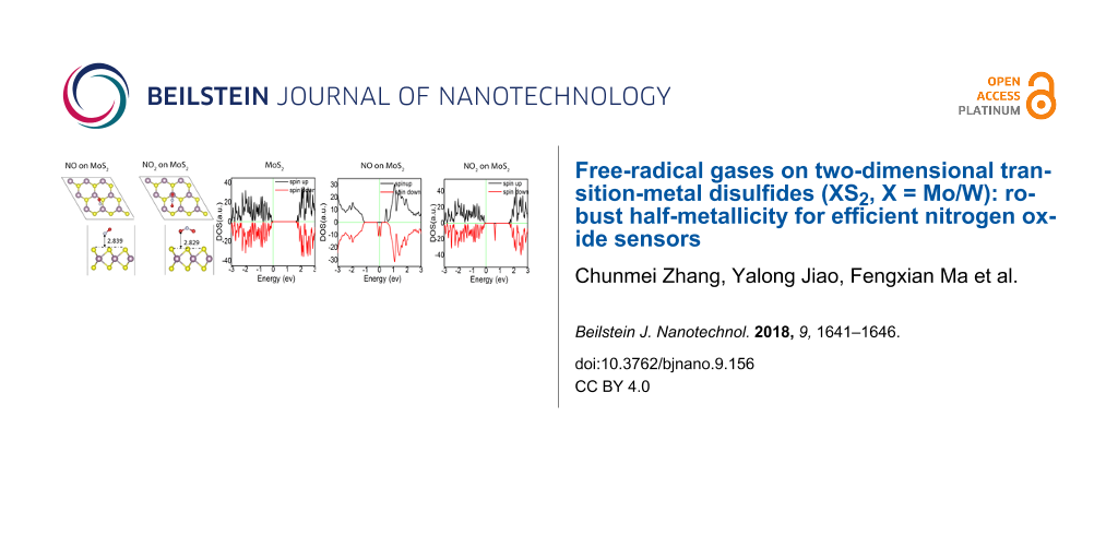
We focus our discussions on the adsorption of NO and NO2 on XS2 (X = Mo, W), as NO and NO2 are paramagnetic free radicals. Most other gas molecules, such as NH3, CO and CO2, have no magnetic moment. Monolayer XS2 (X = Mo, W) have a hexagonal configuration, where three pairs of S atoms are anchored on one X atom and form alternating corners (S–X–S) in a honeycomb network. Figure 1 illustrates the top and side view structures of the favorable NO and NO2 adsorption position on the 3 × 3 supercell of XS2 (X = Mo, W), and Table 1 summarizes the corresponding values of adsorption energy and magnetic moment. The equilibrium height is defined as the vertical distance between N (NO), O (NO2) and the top S-layer of the XS2 (X = Mo, W) sheet (see Figure 1). The calculation based on a 3 × 3 supercell of monolayer XS2, with a single gas molecule adsorbed on it, is chosen as the computational model. A different gas concentration including the model of a unit cell and 6 × 6 supercell with a single gas molecule adsorbed on the surface are also computed (Figure S2, Supporting Information File 1). In Figure 1, the favorable adsorption configuration for NO is the N atom on top of the X–S bond. N is adjacent to S atoms at the monolayer with a distance of 2.839 and 2.735 Å for single-layer MoS2 and WS2, resulting in adsorption energies of −180 and −165 meV (calculated from Equation 1), respectively. NO2 is bonded with the O atoms close to the monolayer with adsorption distances of 2.829 and 2.931 Å, and adsorption energies of −233 and −201meV, respectively, for single-layer MoS2 and WS2 (Figure 1). An adsorption distance of approximately 3 Å suggests that NO and NO2 are physically adsorbed.
![[2190-4286-9-156-1]](/bjnano/content/figures/2190-4286-9-156-1.png?scale=2.0&max-width=1024&background=FFFFFF)
Figure 1: Top and side views of the most favorable NO and NO2 adsorption configurations on monolayers of MoS2 and WS2. The yellow, purple, grey, white and red balls represent S, Mo, W, N, and O atoms, respectively.
Figure 1: Top and side views of the most favorable NO and NO2 adsorption configurations on monolayers of MoS2...
After determining the most favorable adsorption positions, we calculated the electronic properties after the adsorption of NO and NO2. Both NO and NO2 are free radical gas molecules with a magnetic moment of 1µB. To fully understand the NOx adsorption mechanism, it is important to understand the interactions between the monolayer and the adsorbate molecules. Investigations [8,28] revealed that charge transfer occurs from the XS2 (X = Mo, W) nanosheet to the physically adsorbed gas molecules. With the calculated favorable configuration, we compute the corresponding magnetic charge density, total density of state (TDOS) as well as PDOS (Figure S3, Supporting Information File 1) for pristine 2D XS2 (X = Mo, W) and 2D XS2 (X = Mo, W) with adsorbed NOx (x = 1, 2; Figure 2). Pristine 2D XS2 (X = Mo, W) has a band gap of approximately 2 eV. In the case of NO adsorbed on XS2 (X = Mo, W), a large density of spin-up electrons appear around the Fermi level, while no spin-down electrons appear. Analyzing the PDOS of a WS2 nanosheet with adsorbed NO (Figure S3a–d; Supporting Information File 1), we conclude that the N and O p-orbitals result in absolute spin polarization. In the WS2 monolayer with adsorbed NO2, no apparent DOS peaks are present around the Fermi level (Figure 2f). The spatial magnetic charge distribution analysis suggests that all the spin-unpaired electrons are localized on the NO and NO2 molecule (insets of Figure 2b,c,e,f) [30].
![[2190-4286-9-156-2]](/bjnano/content/figures/2190-4286-9-156-2.png?scale=2.0&max-width=1024&background=FFFFFF)
Figure 2: (a–c) TDOS and magnetic charge distribution of (a) the pristine MoS2 monolayer, and MOS2 with (b) adsorbed NO and (c) adsorbed NO2. (d–f) TDOS and magnetic charge distribution of (d) the pristine WS2 monolayer, and WS2 with (e) adsorbed NO and (f) adsorbed NO2. The Fermi level is indicated by the vertical green line.
Figure 2: (a–c) TDOS and magnetic charge distribution of (a) the pristine MoS2 monolayer, and MOS2 with (b) a...
The concept of Fermi-level pinning is usually used in the metal–semiconductor interface region. Zhou et al. [28] Introduced the concept of Fermi-level pinning into the field of gas/2D nanomaterial systems. However, they failed to point out the spin-polarized Fermi-level pinning in gas/2D nanomaterial system. Based on this, we take the single-layer WS2 as an example to elucidate the different Fermi-level pinning processes of adsorption of NO and NO2. The spin orbital-resolved band structures are simulated (Figure 3) and the Fermi level of the adsorbed gas (NO and NO2)/WS2 nanomaterial system is pinned around the lowest unoccupied molecular orbital (LUMO) or highest occupied molecular orbital (HOMO) of the adsorbed gas molecules. The PDOS for WS2 with adsorbed NO indicates that the W and S atoms have no spin polarization (Figure S3c,d; Supporting Information File 1) and the dominant contribution to the HOMO and the LUMO at the Fermi level originates from the p-orbitals of N and O gas atoms (Figure S3a,b; Supporting Information File 1). Therefore, only the p-orbitals of N and O atoms are plotted in Figure 3. For NO adsorption, only the spin-up p-orbitals (red line in Figure 3a) are pinned around the Fermi level, while the spin-down p-orbitals (green line in Figure 3b) are pinned about 0.5 eV above the Fermi level indicating that the electrical current is completely spin-polarized, which is known as half-metallicity. Therefore, the WS2 monolayer with adsorbed NO is ideal for spintronic applications since it has one metallic spin channel and one semiconducting spin channel. After NO2 adsorption (Figure 3b), the spin-down and spin-up p-orbitals of the N and O atoms are pinned approximately 0.5 and 2 eV above the Fermi level, respectively. Some impurity states of WS2 are pinned slightly below the Fermi level upon adsorption of NO2. These impurity states come from the hybridization of spin-up and spin-down orbitals of the W and S atoms (Figure 3c–e), which contribute to the current flow and fail to enable NO2/2D WS2 system display half-metallicity.
![[2190-4286-9-156-3]](/bjnano/content/figures/2190-4286-9-156-3.png?scale=2.0&max-width=1024&background=FFFFFF)
Figure 3: Spin orbital-resolved band structures for WS2 with (a) adsorbed NO and (b–e) adsorbed NO2. The red and green lines represent the contributions from the spin-up and spin-down p-orbitals of N and O atoms. Cyan lines and brown lines represent the contributions from the spin-up and spin-down p-orbitals of S atoms. Yellow lines and blue lines represent the contributions from the spin-down and spin-up orbitals of W atoms. The Fermi level is set to the energy zero point.
Figure 3: Spin orbital-resolved band structures for WS2 with (a) adsorbed NO and (b–e) adsorbed NO2. The red ...
In an attempt to address the selectivity towards NO gas in moist environments, we have carried out some new calculations on the adsorption of NOx (x = 1, 2) on the WS2 monolayer in the presence of a water molecule. The structures and spin-polarized TDOS for 2D WS2 with adsorbed NOx in humid environment are given in Figure S4 (Supporting Information File 1) and Figure 4, respectively. It can be seen that in humid environment, the spin-polarized current is still presented in the WS2 nanosheet with adsorbed NO (Figure 4b) around the Fermi surface, while no apparent spin-polarized current appears when NO2 is adsorbed (Figure 4b) or in the pristine WS2 monolayer (Figure 4a). This shows that the half-metallic property for WS2 with adsorbed NO can be detected even in a humid environment. The water adsorption energy and distance are around −190 meV and 3 Å, suggesting that water is physically adsorbed on the surface of the WS2 nanosheet.
![[2190-4286-9-156-4]](/bjnano/content/figures/2190-4286-9-156-4.png?scale=2.0&max-width=1024&background=FFFFFF)
Figure 4: TDOS of (a) the pristine WS2 monolayer, and the WS2 monolayer with (b) NO adsorbed and (c) NO2 adsorbed in humid environment. The Fermi level is indicated by the vertical green line.
Figure 4: TDOS of (a) the pristine WS2 monolayer, and the WS2 monolayer with (b) NO adsorbed and (c) NO2 adso...
Monolayer MoS2 [38] and multilayer MoS2 field effect transistors [17] for sensing NO at room temperature have been fabricated experimentally. In this work, the ab initio molecular dynamics simulations at room temperature (300 K) for a 3 × 3 supercell model were performed to further evaluate the thermal stability of MoS2 with and without the adsorption of NOx (x = 1, 2) as shown in Figure S5 (Supporting Information File 1). There is no significant structural distortion within 7 ps for the adsorption of NOx onto MoS2, indicating highly thermal stability.”
Conclusion
We have presented monolayer XS2 (X = Mo, W) as NO sensor based on first principles studies. The adsorption sites and energy for NO and NO2 molecules on MoS2 or WS2 layers have been studied. The calculations were carried out with different gas concentrations to confirm that the predicted half-metallicity is indeed robust. Differences in electronic properties and orbital analysis between NO and NO2 adsorption show that half-metallicity is only observed when NO is adsorbed. Since single/multi-layer MoS2 FET sensors for NO have been experimentally obtained, our strategy to detect gas molecules is promising to be applicable.
Supporting Information
| Supporting Information File 1: Additional computational data. | ||
| Format: PDF | Size: 796.7 KB | Download |
Acknowledgements
We acknowledge generous grants of high-performance computer time from the Computing Facility at the Queensland University of Technology, The Pawsey Supercomputing Centre and Australian National Facility. A.D. greatly appreciates the Australian Research Council QEII Fellowship (DP110101239) and financial support of Australian Research Council under Discovery Project (DP130102420 and DP170103598).
References
-
Ko, G.; Kim, H.-Y.; Ahn, J.; Park, Y.-M.; Lee, K.-Y.; Kim, J. Curr. Appl. Phys. 2010, 10, 1002–1004. doi:10.1016/j.cap.2009.12.024
Return to citation in text: [1] -
Ho, K.-C.; Tsou, Y.-H. Sens. Actuators, B 2001, 77, 253–259. doi:10.1016/S0925-4005(01)00742-0
Return to citation in text: [1] -
Zhang, W.; Uchida, H.; Katsube, T.; Nakatsubo, T.; Nishioka, Y. Sens. Actuators 1998, 49, 58–62. doi:10.1016/S0925-4005(98)00129-4
Return to citation in text: [1] -
Yamada, T.; Zhou, H.-S.; Uchida, H.; Tomita, M.; Ueno, Y.; Ichino, T.; Honma, I.; Asai, K.; Katsube, T. Adv. Mater. 2002, 14, 812–815. doi:10.1002/1521-4095(20020605)14:11<812::AID-ADMA812>3.0.CO;2-W
Return to citation in text: [1] -
Yang, Y.; Tian, C.; Wang, J.; Sun, L.; Shi, K.; Zhou, W.; Fu, H. Nanoscale 2014, 6, 7369–7378. doi:10.1039/c4nr00196f
Return to citation in text: [1] -
Yu, F.; Wang, T.; Wen, Z.; Wang, H. J. Power Sources 2017, 364, 9–15. doi:10.1016/j.jpowsour.2017.08.013
Return to citation in text: [1] -
Tang, Q.; Zhou, Z.; Chen, Z. J. Phys. Chem. C 2012, 116, 4119–4125. doi:10.1021/jp211779w
Return to citation in text: [1] -
Leenaerts, O.; Partoens, B.; Peeters, F. M. Phys. Rev. B 2008, 77, 125416. doi:10.1103/PhysRevB.77.125416
Return to citation in text: [1] [2] [3] -
Kou, L.; Frauenheim, T.; Chen, C. J. Phys. Chem. Lett. 2014, 5, 2675–2681. doi:10.1021/jz501188k
Return to citation in text: [1] [2] -
Dong, H.; Wang, L.; Zhou, L.; Hou, T.; Li, Y. Carbon 2017, 113, 114–121. doi:10.1016/j.carbon.2016.11.029
Return to citation in text: [1] [2] -
Zhao, S.; Xue, J.; Kang, W. Chem. Phys. Lett. 2014, 595–596, 35–42. doi:10.1016/j.cplett.2014.01.043
Return to citation in text: [1] [2] [3] -
Liu, H.; Li, X.; Chen, L.; Wang, X.; Pan, H.; Zhang, X.; Zhao, M. J. Phys. Chem. C 2016, 120, 3846–3852. doi:10.1021/acs.jpcc.5b11699
Return to citation in text: [1] -
Wu, G.; Yang, M.; Guo, X.; Wang, J. J. Comput. Chem. 2012, 33, 1854–1861. doi:10.1002/jcc.23017
Return to citation in text: [1] -
Zhang, C.; Jiao, Y.; Ma, F.; Bottle, S.; Zhao, M.; Chen, Z.; Du, A. Phys. Chem. Chem. Phys. 2017, 19, 5449–5453. doi:10.1039/C7CP00157F
Return to citation in text: [1] -
Zhang, C.; Jiao, Y.; He, T.; Ma, F.; Kou, L.; Liao, T.; Bottle, S.; Du, A. Phys. Chem. Chem. Phys. 2017, 19, 25886–25890. doi:10.1039/C7CP04758D
Return to citation in text: [1] -
Rigoni, F.; Maiti, R.; Baratto, C.; Donarelli, M.; MacLeod, J.; Gupta, B.; Lyu, M.; Ponzoni, A.; Sberveglieri, G.; Motta, N.; Faglia, G. Nanotechnology 2017, 28, 414001. doi:10.1088/1361-6528/aa8611
Return to citation in text: [1] -
Li, H.; Yin, Z.; He, Q.; Li, H.; Huang, X.; Lu, G.; Fam, D. W. H.; Tok, A. I. Y.; Zhang, Q.; Zhang, H. Small 2012, 8, 63–67. doi:10.1002/smll.201101016
Return to citation in text: [1] [2] [3] -
Huo, N.; Yang, S.; Wei, Z.; Li, S.-S.; Xia, J.-B.; Li, J. Sci. Rep. 2014, 4, 5209. doi:10.1038/srep05209
Return to citation in text: [1] [2] -
Zhang, W.; Huang, J.-K.; Chen, C.-H.; Chang, Y.-H.; Cheng, Y.-J.; Li, L.-J. Adv. Mater. 2013, 25, 3456–3461. doi:10.1002/adma.201301244
Return to citation in text: [1] -
Perkins, F. K.; Friedman, A. L.; Cobas, E.; Campbell, P. M.; Jernigan, G. G.; Jonker, B. T. Nano Lett. 2013, 13, 668–673. doi:10.1021/nl3043079
Return to citation in text: [1] -
Bryden, J. H. Acta Crystallogr. 1962, 15, 167–171. doi:10.1107/S0365110X62000407
Return to citation in text: [1] -
He, Q.; Zeng, Z.; Yin, Z.; Li, H.; Wu, S.; Huang, X.; Zhang, H. Small 2012, 8, 2994–2999. doi:10.1002/smll.201201224
Return to citation in text: [1] -
Yue, Q.; Shao, Z.; Chang, S.; Li, J. Nanoscale Res. Lett. 2013, 8, 425–432. doi:10.1186/1556-276X-8-425
Return to citation in text: [1] [2] -
Ding, K.; Lin, Y.; Huang, M. Vacuum 2016, 130, 146–153. doi:10.1016/j.vacuum.2016.05.005
Return to citation in text: [1] -
O’Brien, M.; Lee, K.; Morrish, R.; Berner, N. C.; McEvoy, N.; Wolden, C. A.; Duesberg, G. S. Chem. Phys. Lett. 2014, 615, 6–10. doi:10.1016/j.cplett.2014.09.051
Return to citation in text: [1] -
Bui, V. Q.; Pham, T.-T.; Le, D. A.; Thi, C. M.; Le, H. M. J. Phys.: Condens. Matter 2015, 27, 305005. doi:10.1088/0953-8984/27/30/305005
Return to citation in text: [1] -
Sik Hwang, W.; Remskar, M.; Yan, R.; Protasenko, V.; Tahy, K.; Doo Chae, S.; Zhao, P.; Konar, A.; Xing, H.; Seabaugh, A.; Jena, D. Appl. Phys. Lett. 2012, 101, 013107. doi:10.1063/1.4732522
Return to citation in text: [1] -
Zhou, C.; Yang, W.; Zhu, H. J. Chem. Phys. 2015, 142, 214704. doi:10.1063/1.4922049
Return to citation in text: [1] [2] [3] -
Kou, L.; Du, A.; Chen, C.; Frauenheim, T. Nanoscale 2014, 6, 5156–5161. doi:10.1039/C3NR06670C
Return to citation in text: [1] -
Son, Y.-W.; Cohen, M. L.; Louie, S. G. Nature 2006, 444, 347–349. doi:10.1038/nature05180
Return to citation in text: [1] [2] -
Qian, M. C.; Fong, C. Y.; Liu, K.; Pickett, W. E.; Pask, J. E.; Yang, L. H. Phys. Rev. Lett. 2006, 96, 027211. doi:10.1103/PhysRevLett.96.027211
Return to citation in text: [1] -
Kan, E.-J.; Wu, X.; Li, Z.; Zeng, X. C.; Yang, J.; Hou, J. G. J. Chem. Phys. 2008, 129, 084712. doi:10.1063/1.2971187
Return to citation in text: [1] -
Jiao, Y.; Ma, F.; Zhang, C.; Bell, J.; Sanvito, S.; Du, A. Phys. Rev. Lett. 2017, 119, 016403. doi:10.1103/PhysRevLett.119.016403
Return to citation in text: [1] -
Kresse, G.; Hafner, J. Phys. Rev. B 1993, 47, 558–561. doi:10.1103/PhysRevB.47.558
Return to citation in text: [1] -
Kresse, G.; Furthmüller, J. Phys. Rev. B 1996, 54, 11169. doi:10.1103/PhysRevB.54.11169
Return to citation in text: [1] -
Blöchl, P. E. Phys. Rev. B 1994, 50, 17953. doi:10.1103/PhysRevB.50.17953
Return to citation in text: [1] -
Grimme, S. J. Comput. Chem. 2006, 27, 1787–1799. doi:10.1002/jcc.20495
Return to citation in text: [1] -
He, K.; Poole, C.; Mak, K. F.; Shan, J. Nano Lett. 2013, 13, 2931–2936. doi:10.1021/nl4013166
Return to citation in text: [1]
| 1. | Ko, G.; Kim, H.-Y.; Ahn, J.; Park, Y.-M.; Lee, K.-Y.; Kim, J. Curr. Appl. Phys. 2010, 10, 1002–1004. doi:10.1016/j.cap.2009.12.024 |
| 5. | Yang, Y.; Tian, C.; Wang, J.; Sun, L.; Shi, K.; Zhou, W.; Fu, H. Nanoscale 2014, 6, 7369–7378. doi:10.1039/c4nr00196f |
| 18. | Huo, N.; Yang, S.; Wei, Z.; Li, S.-S.; Xia, J.-B.; Li, J. Sci. Rep. 2014, 4, 5209. doi:10.1038/srep05209 |
| 4. | Yamada, T.; Zhou, H.-S.; Uchida, H.; Tomita, M.; Ueno, Y.; Ichino, T.; Honma, I.; Asai, K.; Katsube, T. Adv. Mater. 2002, 14, 812–815. doi:10.1002/1521-4095(20020605)14:11<812::AID-ADMA812>3.0.CO;2-W |
| 27. | Sik Hwang, W.; Remskar, M.; Yan, R.; Protasenko, V.; Tahy, K.; Doo Chae, S.; Zhao, P.; Konar, A.; Xing, H.; Seabaugh, A.; Jena, D. Appl. Phys. Lett. 2012, 101, 013107. doi:10.1063/1.4732522 |
| 3. | Zhang, W.; Uchida, H.; Katsube, T.; Nakatsubo, T.; Nishioka, Y. Sens. Actuators 1998, 49, 58–62. doi:10.1016/S0925-4005(98)00129-4 |
| 11. | Zhao, S.; Xue, J.; Kang, W. Chem. Phys. Lett. 2014, 595–596, 35–42. doi:10.1016/j.cplett.2014.01.043 |
| 2. | Ho, K.-C.; Tsou, Y.-H. Sens. Actuators, B 2001, 77, 253–259. doi:10.1016/S0925-4005(01)00742-0 |
| 17. | Li, H.; Yin, Z.; He, Q.; Li, H.; Huang, X.; Lu, G.; Fam, D. W. H.; Tok, A. I. Y.; Zhang, Q.; Zhang, H. Small 2012, 8, 63–67. doi:10.1002/smll.201101016 |
| 9. | Kou, L.; Frauenheim, T.; Chen, C. J. Phys. Chem. Lett. 2014, 5, 2675–2681. doi:10.1021/jz501188k |
| 11. | Zhao, S.; Xue, J.; Kang, W. Chem. Phys. Lett. 2014, 595–596, 35–42. doi:10.1016/j.cplett.2014.01.043 |
| 17. | Li, H.; Yin, Z.; He, Q.; Li, H.; Huang, X.; Lu, G.; Fam, D. W. H.; Tok, A. I. Y.; Zhang, Q.; Zhang, H. Small 2012, 8, 63–67. doi:10.1002/smll.201101016 |
| 8. | Leenaerts, O.; Partoens, B.; Peeters, F. M. Phys. Rev. B 2008, 77, 125416. doi:10.1103/PhysRevB.77.125416 |
| 16. | Rigoni, F.; Maiti, R.; Baratto, C.; Donarelli, M.; MacLeod, J.; Gupta, B.; Lyu, M.; Ponzoni, A.; Sberveglieri, G.; Motta, N.; Faglia, G. Nanotechnology 2017, 28, 414001. doi:10.1088/1361-6528/aa8611 |
| 18. | Huo, N.; Yang, S.; Wei, Z.; Li, S.-S.; Xia, J.-B.; Li, J. Sci. Rep. 2014, 4, 5209. doi:10.1038/srep05209 |
| 19. | Zhang, W.; Huang, J.-K.; Chen, C.-H.; Chang, Y.-H.; Cheng, Y.-J.; Li, L.-J. Adv. Mater. 2013, 25, 3456–3461. doi:10.1002/adma.201301244 |
| 20. | Perkins, F. K.; Friedman, A. L.; Cobas, E.; Campbell, P. M.; Jernigan, G. G.; Jonker, B. T. Nano Lett. 2013, 13, 668–673. doi:10.1021/nl3043079 |
| 21. | Bryden, J. H. Acta Crystallogr. 1962, 15, 167–171. doi:10.1107/S0365110X62000407 |
| 22. | He, Q.; Zeng, Z.; Yin, Z.; Li, H.; Wu, S.; Huang, X.; Zhang, H. Small 2012, 8, 2994–2999. doi:10.1002/smll.201201224 |
| 23. | Yue, Q.; Shao, Z.; Chang, S.; Li, J. Nanoscale Res. Lett. 2013, 8, 425–432. doi:10.1186/1556-276X-8-425 |
| 24. | Ding, K.; Lin, Y.; Huang, M. Vacuum 2016, 130, 146–153. doi:10.1016/j.vacuum.2016.05.005 |
| 25. | O’Brien, M.; Lee, K.; Morrish, R.; Berner, N. C.; McEvoy, N.; Wolden, C. A.; Duesberg, G. S. Chem. Phys. Lett. 2014, 615, 6–10. doi:10.1016/j.cplett.2014.09.051 |
| 26. | Bui, V. Q.; Pham, T.-T.; Le, D. A.; Thi, C. M.; Le, H. M. J. Phys.: Condens. Matter 2015, 27, 305005. doi:10.1088/0953-8984/27/30/305005 |
| 7. | Tang, Q.; Zhou, Z.; Chen, Z. J. Phys. Chem. C 2012, 116, 4119–4125. doi:10.1021/jp211779w |
| 8. | Leenaerts, O.; Partoens, B.; Peeters, F. M. Phys. Rev. B 2008, 77, 125416. doi:10.1103/PhysRevB.77.125416 |
| 9. | Kou, L.; Frauenheim, T.; Chen, C. J. Phys. Chem. Lett. 2014, 5, 2675–2681. doi:10.1021/jz501188k |
| 10. | Dong, H.; Wang, L.; Zhou, L.; Hou, T.; Li, Y. Carbon 2017, 113, 114–121. doi:10.1016/j.carbon.2016.11.029 |
| 11. | Zhao, S.; Xue, J.; Kang, W. Chem. Phys. Lett. 2014, 595–596, 35–42. doi:10.1016/j.cplett.2014.01.043 |
| 12. | Liu, H.; Li, X.; Chen, L.; Wang, X.; Pan, H.; Zhang, X.; Zhao, M. J. Phys. Chem. C 2016, 120, 3846–3852. doi:10.1021/acs.jpcc.5b11699 |
| 13. | Wu, G.; Yang, M.; Guo, X.; Wang, J. J. Comput. Chem. 2012, 33, 1854–1861. doi:10.1002/jcc.23017 |
| 14. | Zhang, C.; Jiao, Y.; Ma, F.; Bottle, S.; Zhao, M.; Chen, Z.; Du, A. Phys. Chem. Chem. Phys. 2017, 19, 5449–5453. doi:10.1039/C7CP00157F |
| 15. | Zhang, C.; Jiao, Y.; He, T.; Ma, F.; Kou, L.; Liao, T.; Bottle, S.; Du, A. Phys. Chem. Chem. Phys. 2017, 19, 25886–25890. doi:10.1039/C7CP04758D |
| 6. | Yu, F.; Wang, T.; Wen, Z.; Wang, H. J. Power Sources 2017, 364, 9–15. doi:10.1016/j.jpowsour.2017.08.013 |
| 10. | Dong, H.; Wang, L.; Zhou, L.; Hou, T.; Li, Y. Carbon 2017, 113, 114–121. doi:10.1016/j.carbon.2016.11.029 |
| 29. | Kou, L.; Du, A.; Chen, C.; Frauenheim, T. Nanoscale 2014, 6, 5156–5161. doi:10.1039/C3NR06670C |
| 23. | Yue, Q.; Shao, Z.; Chang, S.; Li, J. Nanoscale Res. Lett. 2013, 8, 425–432. doi:10.1186/1556-276X-8-425 |
| 28. | Zhou, C.; Yang, W.; Zhu, H. J. Chem. Phys. 2015, 142, 214704. doi:10.1063/1.4922049 |
| 38. | He, K.; Poole, C.; Mak, K. F.; Shan, J. Nano Lett. 2013, 13, 2931–2936. doi:10.1021/nl4013166 |
| 17. | Li, H.; Yin, Z.; He, Q.; Li, H.; Huang, X.; Lu, G.; Fam, D. W. H.; Tok, A. I. Y.; Zhang, Q.; Zhang, H. Small 2012, 8, 63–67. doi:10.1002/smll.201101016 |
| 30. | Son, Y.-W.; Cohen, M. L.; Louie, S. G. Nature 2006, 444, 347–349. doi:10.1038/nature05180 |
| 28. | Zhou, C.; Yang, W.; Zhu, H. J. Chem. Phys. 2015, 142, 214704. doi:10.1063/1.4922049 |
| 8. | Leenaerts, O.; Partoens, B.; Peeters, F. M. Phys. Rev. B 2008, 77, 125416. doi:10.1103/PhysRevB.77.125416 |
| 28. | Zhou, C.; Yang, W.; Zhu, H. J. Chem. Phys. 2015, 142, 214704. doi:10.1063/1.4922049 |
| 30. | Son, Y.-W.; Cohen, M. L.; Louie, S. G. Nature 2006, 444, 347–349. doi:10.1038/nature05180 |
| 31. | Qian, M. C.; Fong, C. Y.; Liu, K.; Pickett, W. E.; Pask, J. E.; Yang, L. H. Phys. Rev. Lett. 2006, 96, 027211. doi:10.1103/PhysRevLett.96.027211 |
| 32. | Kan, E.-J.; Wu, X.; Li, Z.; Zeng, X. C.; Yang, J.; Hou, J. G. J. Chem. Phys. 2008, 129, 084712. doi:10.1063/1.2971187 |
| 33. | Jiao, Y.; Ma, F.; Zhang, C.; Bell, J.; Sanvito, S.; Du, A. Phys. Rev. Lett. 2017, 119, 016403. doi:10.1103/PhysRevLett.119.016403 |
| 34. | Kresse, G.; Hafner, J. Phys. Rev. B 1993, 47, 558–561. doi:10.1103/PhysRevB.47.558 |
| 35. | Kresse, G.; Furthmüller, J. Phys. Rev. B 1996, 54, 11169. doi:10.1103/PhysRevB.54.11169 |
| 36. | Blöchl, P. E. Phys. Rev. B 1994, 50, 17953. doi:10.1103/PhysRevB.50.17953 |
© 2018 Zhang et al.; licensee Beilstein-Institut.
This is an Open Access article under the terms of the Creative Commons Attribution License (http://creativecommons.org/licenses/by/4.0), which permits unrestricted use, distribution, and reproduction in any medium, provided the original work is properly cited.
The license is subject to the Beilstein Journal of Nanotechnology terms and conditions: (https://www.beilstein-journals.org/bjnano)