Abstract
In piezoelectric semiconductors, electric fields drive carriers into motion/redistribution, and in turn the carrier motion/redistribution has an opposite effect on the electric field itself. Thus, carrier drift in a piezoelectric semiconducting structure is essentially nonlinear unless the induced fluctuation of carrier concentration is very small. In this paper, the nonlinear governing equation of carrier concentration was established by coupling both piezoelectric effect and semiconduction. A nonlinear carrier-drift effect on the performance of a ZnO nanogenerator was investigated in detail and it was elucidated that carrier motion/redistribution occurs in the ZnO nanowire (ZNW) cross section while there is no carrier motion in the axial direction. At the same time, we noted that the amplitude of boundary electric charge grows with increasing deformation, but the peaks of boundary electric charge do not appear at the cross-section endpoints. Thus, in order to effectively improve the performance of the ZNW nanogenerator, the effect of electrode configuration on the piezoelectric potential difference and output power was analyzed in detail. The electrode size for the optimal performance of a ZnO nanowire generator was proposed. This analysis that couples electromechanical fields and carrier concentration as a whole has some referential significance to piezotronics.
Introduction
An acoustic wave propagating in piezoelectric semiconductors usually stimulates electric fields that bring charge carriers into motion, and conversely, the carrier motion will produce an opposite effect on the electric fields and the acoustic wave itself [1-4]. This kind of interaction between an acoustic wave and carriers in piezoelectric semiconductors is called the acoustoelectric effect, which is a special case of a more general phenomenon, called wave–particle drag [4,5]. Obviously, acoustoelectric coupling of piezoelectric semiconductors can be used to develop many new microelectronic devices with modern functions, for example piezoelectric field-effect transistors [6-11], piezoelectric charge-coupled devices [12-15], piezoelectric chemical sensors [16,17], and nanogenerators made of vertically aligned ZnO nanowires [18-27]. The principle of nanogenerators is that the piezoelectric potential produced by the piezoelectric effect can produce a current in an external circuit when the ZNW is deformed. Specifically, a transversely applied force makes the nanowire bent when an atomic force microscopy tip scans over the top of the nanowire. The electromechanical coupling converts mechanical energy into electric energy [28,29]. A piezoelectric potential is built inside the nanowire with the stretched side being positively charged and the compressed side being negatively charged. At the same time, a Schottky barrier formed between the AFM tip and the nanowire and the piezoelectric potential will not disappear as long as the mechanical stress is maintained. This potential can be made use of to generate an electrical current [30].
Recently, Fan et al. studied the linear solutions of electromechanical quantities in a bent ZNW under the assumption of a small fluctuation of the carrier concentration [31]. Electric fields are proven to be independent of the axial position along the c-axis except near the end regions, and carrier motion/redistribution is proven to occur along the cross section. Because the semiconduction in ZNWs results in some electric leakage, a smaller initial carrier concentration is suggested to be more proper for energy-harvesting from a bent ZNW [31]. Because a small fluctuation of the carrier concentration implies a small deformation, a very low output of ZNW nanogenerators occurs under that situation. The force necessarily to obtain a good performance of the nanogenerator will certainly result in large variations of carrier concentration [30]. Thus, we abandon the assumption of small carrier-concentration fluctuations and establish the corresponding nonlinear governing equation of carrier concentration in this paper. The nonlinear accumulation of n-type carriers on one side of the ZNW cross section is shown in detail. Distribution characteristics of carrier concentration and electric potential in the cross section are discussed. Both the boundary electric charge and the boundary electric potential difference are calculated in depth. It is found that the amplitude of boundary electric charge always grows with increasing deformation, but the peaks of boundary electric charge do not appear directly at the cross-section endpoints. For harvesting a bent beam-like structure, the output electrodes are usually placed near the two cross section endpoints [30,32,33]. To improve the performance of a ZNW nanogenerator, the electrode configuration should be optimized with regard to piezoelectric potential difference and output power. We also carry out a detailed analysis on the effect of the electrode configuration.
Nonlinear Governing Equation of Carrier Concentration for a Bent ZNW
In a bent ZnO nanowire as shown in Figure 1, elastic fields can be solved in advance by using the irrotationality of static electric fields [31]. The two in-plane electric field components, E1 and E2, can be proven only to depend on x1 and x2, while the out-of-plane component E3 is zero. The electric displacements, D = (D1, D2, D3)T, in the ZNW are:
![[2190-4286-9-183-i1]](/bjnano/content/inline/2190-4286-9-183-i1.svg?max-width=590&scale=1.18182)
with
![[2190-4286-9-183-i2]](/bjnano/content/inline/2190-4286-9-183-i2.svg?max-width=590&scale=1.18182)
where ![[Graphic 1]](/bjnano/content/inline/2190-4286-9-183-i14.svg?max-width=637&scale=1.18182) are the compliance coefficients with cKL being the elastic constants; εij being the dielectric constants and eiL being the electromechanical coupling coefficients. K, L = 1, 2,…, 6; i, j = 1, 2, 3;
are the compliance coefficients with cKL being the elastic constants; εij being the dielectric constants and eiL being the electromechanical coupling coefficients. K, L = 1, 2,…, 6; i, j = 1, 2, 3; ![[Graphic 2]](/bjnano/content/inline/2190-4286-9-183-i15.svg?max-width=637&scale=1.18182) The cross section of a bent ZnO nanowire is assumed to be circular in our analysis, which was also assumed by, for example, Gao and Wang [26,27], Henneghien et al. [34], and Maslov and co-workers [35]. In particular, Henneghien et al. have pointed out that circular and hexagonal nanowires exhibit the same behavior if the ZnO nanowire sections of each structure have the same area.
The cross section of a bent ZnO nanowire is assumed to be circular in our analysis, which was also assumed by, for example, Gao and Wang [26,27], Henneghien et al. [34], and Maslov and co-workers [35]. In particular, Henneghien et al. have pointed out that circular and hexagonal nanowires exhibit the same behavior if the ZnO nanowire sections of each structure have the same area.
![[2190-4286-9-183-1]](/bjnano/content/figures/2190-4286-9-183-1.png?scale=2.0&max-width=1024&background=FFFFFF)
Figure 1: A circular ZNW cantilever exposed to a force P at the free end.
Figure 1: A circular ZNW cantilever exposed to a force P at the free end.
Linear solutions were obtained for small fluctuations of carrier concentration in a bent n-type ZnO nanowire under a force P = 0.7 nN at the end of the nanowire [31]. However, small carrier concentration fluctuations, ![[Graphic 3]](/bjnano/content/inline/2190-4286-9-183-i16.svg?max-width=637&scale=1.18182) where Δn = n − n0, imply a very low output of the ZNW generator under consideration. Here, n and n0 stand for the actual and the initial carrier concentration, respectively. P should be enlarged for obtaining a better performance of the nanogenerator. Electric fields appearing in piezoelectric semiconductors will move/redistribute carriers and, in turn, the motion/redistribution of carriers will have an influence on the electric fields. This indicates that the first carrier drift term in the electric current expression, Ji = qnμijEj + qκijn,j, is essentially nonlinear. Since a ZNW with the crystallographic c-axis along the x3-direction is transversely isotropic, the electron mobility μij and the diffusion coefficients κij can be written as
where Δn = n − n0, imply a very low output of the ZNW generator under consideration. Here, n and n0 stand for the actual and the initial carrier concentration, respectively. P should be enlarged for obtaining a better performance of the nanogenerator. Electric fields appearing in piezoelectric semiconductors will move/redistribute carriers and, in turn, the motion/redistribution of carriers will have an influence on the electric fields. This indicates that the first carrier drift term in the electric current expression, Ji = qnμijEj + qκijn,j, is essentially nonlinear. Since a ZNW with the crystallographic c-axis along the x3-direction is transversely isotropic, the electron mobility μij and the diffusion coefficients κij can be written as
![[2190-4286-9-183-i3]](/bjnano/content/inline/2190-4286-9-183-i3.svg?max-width=590&scale=1.18182)
The two in-plane components of the electric field can thus be obtained from Ji = qnμijEj + qκijn,j = 0, the null-current condition, as follows with ζ = κ11/μ11:
![[2190-4286-9-183-i4]](/bjnano/content/inline/2190-4286-9-183-i4.svg?max-width=590&scale=1.18182)
Substituting Equation 4 into Equation 1 and then into the Gauss law, ![[Graphic 4]](/bjnano/content/inline/2190-4286-9-183-i17.svg?max-width=637&scale=1.18182) , yields the nonlinear governing equation of carrier concentration
, yields the nonlinear governing equation of carrier concentration ![[Graphic 5]](/bjnano/content/inline/2190-4286-9-183-i18.svg?max-width=637&scale=1.18182) as
as
![[2190-4286-9-183-i5]](/bjnano/content/inline/2190-4286-9-183-i5.svg?max-width=590&scale=1.18182)
where ![[Graphic 6]](/bjnano/content/inline/2190-4286-9-183-i19.svg?max-width=637&scale=1.18182) and
and
![[2190-4286-9-183-i6]](/bjnano/content/inline/2190-4286-9-183-i6.svg?max-width=590&scale=1.18182)
In the vacuum outside the ZNW cross-section, the electric potential ![[Graphic 7]](/bjnano/content/inline/2190-4286-9-183-i20.svg?max-width=637&scale=1.18182) should satisfy
should satisfy
![[2190-4286-9-183-i7]](/bjnano/content/inline/2190-4286-9-183-i7.svg?max-width=590&scale=1.18182)
The point of zero electric potential is set at infinity, i.e., ![[Graphic 8]](/bjnano/content/inline/2190-4286-9-183-i21.svg?max-width=637&scale=1.18182) . The continuous conditions of normal electric displacement
. The continuous conditions of normal electric displacement ![[Graphic 9]](/bjnano/content/inline/2190-4286-9-183-i22.svg?max-width=637&scale=1.18182) and electric potential
and electric potential ![[Graphic 10]](/bjnano/content/inline/2190-4286-9-183-i23.svg?max-width=637&scale=1.18182) at the boundary Ω, r = a, of the ZNW cross section require
at the boundary Ω, r = a, of the ZNW cross section require
![[2190-4286-9-183-i8]](/bjnano/content/inline/2190-4286-9-183-i8.svg?max-width=590&scale=1.18182)
where ![[Graphic 11]](/bjnano/content/inline/2190-4286-9-183-i24.svg?max-width=637&scale=1.18182) refers to the electric potential within the ZNW cross section, and r and θ stand for the radial and the tangential coordinate, respectively, as shown in Figure 1. ε0 is the dielectric coefficient of the vacuum.
refers to the electric potential within the ZNW cross section, and r and θ stand for the radial and the tangential coordinate, respectively, as shown in Figure 1. ε0 is the dielectric coefficient of the vacuum.
Results and Discussion
We calculate carrier concentration fluctuation, piezoelectric potential, electric fields, boundary charges by using the finite element method for P from 0.7 nN to 80 nN, where the ZnO nanowire has a diameter d = 50 nm and its c-axis is oriented along the x3-direction. The material constants are given below in Equation 9 [36-41] with ε0 = 8.8542·10−12 F/ m.
![[2190-4286-9-183-i9]](/bjnano/content/inline/2190-4286-9-183-i9.svg?max-width=590&scale=1.18182)
For a bent n-type ZNW in the linear regime, a positive piezoelectric potential appears at the stretched side and negative piezoelectric potential appears at the compressed side [26-31], i.e., the electric potential is high at ![[Graphic 12]](/bjnano/content/inline/2190-4286-9-183-i25.svg?max-width=637&scale=1.18182) and low at
and low at ![[Graphic 13]](/bjnano/content/inline/2190-4286-9-183-i26.svg?max-width=637&scale=1.18182) . When the end force P increases, n-type carriers will be driven to drift upwards with an accumulation at the stretched side, Δn/n0, becoming so large that the linear balance regime collapses. Non-uniformity in carrier concentration accompanied by drift will bring about also diffusion. These two effects of drift and diffusion will achieve a new equilibrium at every step of increase in P. A higher accumulation of carriers in
. When the end force P increases, n-type carriers will be driven to drift upwards with an accumulation at the stretched side, Δn/n0, becoming so large that the linear balance regime collapses. Non-uniformity in carrier concentration accompanied by drift will bring about also diffusion. These two effects of drift and diffusion will achieve a new equilibrium at every step of increase in P. A higher accumulation of carriers in ![[Graphic 14]](/bjnano/content/inline/2190-4286-9-183-i27.svg?max-width=637&scale=1.18182) results in a stronger nonlinearity. Figure 2a shows the nonlinearity manifesting itself from carrier drift with n0 = 1.0·1023m−3 for P = 0.7, 1.5, 3.0, 5.0 and 10.0 nN. P = 0.7 nN corresponds to the linear case of which the largest variance of carrier concentration,
results in a stronger nonlinearity. Figure 2a shows the nonlinearity manifesting itself from carrier drift with n0 = 1.0·1023m−3 for P = 0.7, 1.5, 3.0, 5.0 and 10.0 nN. P = 0.7 nN corresponds to the linear case of which the largest variance of carrier concentration, ![[Graphic 15]](/bjnano/content/inline/2190-4286-9-183-i28.svg?max-width=637&scale=1.18182) , appears along the neutral axis [31]. There are two factors to affect
, appears along the neutral axis [31]. There are two factors to affect ![[Graphic 16]](/bjnano/content/inline/2190-4286-9-183-i29.svg?max-width=637&scale=1.18182) : mechanical shear deformations and accumulation of electric carriers. In general, shear deformations result in in-plane electric fields, which lead to carrier drift, while carrier accumulation results in diffusion. Because Δn/n0 is very small in the whole ZNW cross section in the linear regime, the largest variance rate of carrier concentration appears along the neutral axis because of the strongest shear deformation there. With increasing end force, the carrier accumulation increases such that there is a stronger nonlinear drift effect on
: mechanical shear deformations and accumulation of electric carriers. In general, shear deformations result in in-plane electric fields, which lead to carrier drift, while carrier accumulation results in diffusion. Because Δn/n0 is very small in the whole ZNW cross section in the linear regime, the largest variance rate of carrier concentration appears along the neutral axis because of the strongest shear deformation there. With increasing end force, the carrier accumulation increases such that there is a stronger nonlinear drift effect on ![[Graphic 17]](/bjnano/content/inline/2190-4286-9-183-i30.svg?max-width=637&scale=1.18182) . The carrier concentration gradually grows in the upper portion and reduces in the lower portion, which yields
. The carrier concentration gradually grows in the upper portion and reduces in the lower portion, which yields ![[Graphic 18]](/bjnano/content/inline/2190-4286-9-183-i31.svg?max-width=637&scale=1.18182) for
for ![[Graphic 19]](/bjnano/content/inline/2190-4286-9-183-i32.svg?max-width=637&scale=1.18182) and
and ![[Graphic 20]](/bjnano/content/inline/2190-4286-9-183-i33.svg?max-width=637&scale=1.18182) for
for ![[Graphic 21]](/bjnano/content/inline/2190-4286-9-183-i34.svg?max-width=637&scale=1.18182) . Hence, at larger P,
. Hence, at larger P, ![[Graphic 22]](/bjnano/content/inline/2190-4286-9-183-i35.svg?max-width=637&scale=1.18182) becomes larger for
becomes larger for ![[Graphic 23]](/bjnano/content/inline/2190-4286-9-183-i36.svg?max-width=637&scale=1.18182) and smaller for
and smaller for ![[Graphic 24]](/bjnano/content/inline/2190-4286-9-183-i37.svg?max-width=637&scale=1.18182) and the position of the largest variance
and the position of the largest variance ![[Graphic 25]](/bjnano/content/inline/2190-4286-9-183-i38.svg?max-width=637&scale=1.18182) gradually shifts upwards, as shown in Figure 2a. When P becomes very large (Figure 2b, P = 10, 30, 50, 60, 70 and 80 nN for n0 = 1.0·1023m−3), the position of the largest variance shifts upwards even more, implying that most of the carriers are accumulated in the upper cross section.
gradually shifts upwards, as shown in Figure 2a. When P becomes very large (Figure 2b, P = 10, 30, 50, 60, 70 and 80 nN for n0 = 1.0·1023m−3), the position of the largest variance shifts upwards even more, implying that most of the carriers are accumulated in the upper cross section.
![[2190-4286-9-183-2]](/bjnano/content/figures/2190-4286-9-183-2.png?scale=2.0&max-width=1024&background=FFFFFF)
Figure 2: Nonlinearity as a result of carrier drift for n0 = 1.0·1023m−3 as a function of the end force P. a) P = 0.7, 1.5, 3.0, 5.0 and 10.0 nN; b) P = 10, 30, 50, 60, 70 and 80 nN.
Figure 2: Nonlinearity as a result of carrier drift for n0 = 1.0·1023m−3 as a function of the end force P. a)...
Figure 3 shows the carrier distribution in the ZNW cross section for P = 50, 60, 70 and 80 nN. It is easy to find numerically that ![[Graphic 26]](/bjnano/content/inline/2190-4286-9-183-i39.svg?max-width=637&scale=1.18182) . Given the charge-balance condition this results needs to be explained. It is very obvious that there is no drift and diffusion of carriers along the axial x3-direction due to E3 = 0. Carrier drift and diffusion only occur along the cross section. In thermal equilibrium, the Fermi energy level Σf must be consistent in the cross section with the carrier concentration satisfying
. Given the charge-balance condition this results needs to be explained. It is very obvious that there is no drift and diffusion of carriers along the axial x3-direction due to E3 = 0. Carrier drift and diffusion only occur along the cross section. In thermal equilibrium, the Fermi energy level Σf must be consistent in the cross section with the carrier concentration satisfying
![[2190-4286-9-183-i10]](/bjnano/content/inline/2190-4286-9-183-i10.svg?max-width=590&scale=1.18182)
where ni is the intrinsic carrier concentration of ZnO; Σi(x1, x2) stands for the intrinsic energy level that can be affected by the electric potential field; kB is the Boltzmann constant and T is the temperature (300 K in our analysis). n0 = ni·exp[(Σf − Σi(0))/kBT], Σi(0) is the initial intrinsic energy level, which is constant in the whole cross section under P = 0. When the ZNW is bent by a nonzero end force P, Σi(x1,x2) becomes alterable in the cross section in terms of the electric potential field, which turns Equation 10 into
![[2190-4286-9-183-i11]](/bjnano/content/inline/2190-4286-9-183-i11.svg?max-width=590&scale=1.18182)
Equation 11 indicates an exponential relationship between carrier concentration and electric potential in the cross section. Figure 4 shows the distribution of the electric potential in the ZNW cross section for P = 50, 60, 70 and 80 nN, which can also be obtained directly from Figure 3 by using Equation 11. In the electric potential field, ![[Graphic 27]](/bjnano/content/inline/2190-4286-9-183-i40.svg?max-width=637&scale=1.18182) , all n-type carriers in the cross section obtain additional electric potential energy,
, all n-type carriers in the cross section obtain additional electric potential energy, ![[Graphic 28]](/bjnano/content/inline/2190-4286-9-183-i41.svg?max-width=637&scale=1.18182) . This potential energy increases/reduces the energy of electrons there, and thus, increases/decreases the number of the n-type carriers according to Equation 11, i.e., it is the appearance of additional electric potential energy induced by the electric potential field that results in
. This potential energy increases/reduces the energy of electrons there, and thus, increases/decreases the number of the n-type carriers according to Equation 11, i.e., it is the appearance of additional electric potential energy induced by the electric potential field that results in ![[Graphic 29]](/bjnano/content/inline/2190-4286-9-183-i42.svg?max-width=637&scale=1.18182) .
.
![[2190-4286-9-183-3]](/bjnano/content/figures/2190-4286-9-183-3.png?scale=2.0&max-width=1024&background=FFFFFF)
Figure 3: Carrier distribution in the ZNW cross section for P = 50, 60, 70 and 80 nN.
Figure 3: Carrier distribution in the ZNW cross section for P = 50, 60, 70 and 80 nN.
![[2190-4286-9-183-4]](/bjnano/content/figures/2190-4286-9-183-4.png?scale=2.0&max-width=1024&background=FFFFFF)
Figure 4: Distribution of electric potential in the ZNW cross section for P = 50, 60, 70 and 80 nN.
Figure 4: Distribution of electric potential in the ZNW cross section for P = 50, 60, 70 and 80 nN.
It follows from Figure 4 that there is a strong electric potential gradient along the x2-direction, and the maximal electric potential difference is between the two endpoints of the x2-axis. Furthermore, the maximal positive potential amplitude is much lower than the maximal negative potential amplitude. In a bent piezoelectric semiconducting beam, two shear deformations produce two in-plane electric field components, E1 and E2. E1 is induced by the shear strain S5 in the x1–x3 plane and E2 is induced by the shear strain S4 in the x2–x3 plane. When P acts along the x2-direction, σ5(τ13) is very small, and so is S5. Thus, both σ5 and S5 produce negligible influence on electric field, carrier concentration and electric potential. S4 is the primary deformation component to induce the electric field E2 and carrier redistribution. We show in Figure 5 the effect of n0 on E2 in order to understand why the maximal positive potential amplitude is much less than the maximal negative potential amplitude [27]. For comparison, we have also included the electric field E2 induced only by the piezoelectric effect of a ZNW without taking into account semiconduction (marked as “piezo” in the following figures). Independently of the deformation, in a piezoelectric insulator ZNW (without semiconduction) its Fermi energy level is always at the center of the forbidden band. Hence, the electric field E2 induced only by the piezoelectric characteristics is symmetrical with regard to the neutral axis, as shown in Figure 5. After n-type doping, the Fermi level moves upwards from the center of the forbidden band. The deformation-induced electric field induces motion/redistribution of carriers: the positive electric field E2 drives the carriers upwards, i.e., the bottom portion, ![[Graphic 30]](/bjnano/content/inline/2190-4286-9-183-i43.svg?max-width=637&scale=1.18182) , loses carriers and the upper portion,
, loses carriers and the upper portion, ![[Graphic 31]](/bjnano/content/inline/2190-4286-9-183-i44.svg?max-width=637&scale=1.18182) , accumulates carriers. This motion/redistribution of carriers will in turn decrease the positive electric field E2. Moreover, E2 is reduced more at
, accumulates carriers. This motion/redistribution of carriers will in turn decrease the positive electric field E2. Moreover, E2 is reduced more at ![[Graphic 32]](/bjnano/content/inline/2190-4286-9-183-i45.svg?max-width=637&scale=1.18182) than at
than at ![[Graphic 33]](/bjnano/content/inline/2190-4286-9-183-i46.svg?max-width=637&scale=1.18182) . It can be found from Figure 3 that
. It can be found from Figure 3 that ![[Graphic 34]](/bjnano/content/inline/2190-4286-9-183-i47.svg?max-width=637&scale=1.18182) occurs at
occurs at ![[Graphic 35]](/bjnano/content/inline/2190-4286-9-183-i48.svg?max-width=637&scale=1.18182) ≈ −0.236, −0.273, −0.309 and −0.338 for P = 50, 60, 70 and 80 nN, respectively, with n0 = 1.0·1023 m−3. It should be noted that at
≈ −0.236, −0.273, −0.309 and −0.338 for P = 50, 60, 70 and 80 nN, respectively, with n0 = 1.0·1023 m−3. It should be noted that at ![[Graphic 36]](/bjnano/content/inline/2190-4286-9-183-i49.svg?max-width=637&scale=1.18182) ,
, ![[Graphic 37]](/bjnano/content/inline/2190-4286-9-183-i50.svg?max-width=637&scale=1.18182) and the intrinsic energy level is Σi(0). Because
and the intrinsic energy level is Σi(0). Because ![[Graphic 38]](/bjnano/content/inline/2190-4286-9-183-i51.svg?max-width=637&scale=1.18182) is reduced more in the region
is reduced more in the region ![[Graphic 39]](/bjnano/content/inline/2190-4286-9-183-i52.svg?max-width=637&scale=1.18182) than in
than in ![[Graphic 40]](/bjnano/content/inline/2190-4286-9-183-i53.svg?max-width=637&scale=1.18182) , as shown in Figure 5, the amplitude of the positive electric potential at
, as shown in Figure 5, the amplitude of the positive electric potential at ![[Graphic 41]](/bjnano/content/inline/2190-4286-9-183-i54.svg?max-width=637&scale=1.18182) becomes much smaller than the amplitude of the negative electric potential at
becomes much smaller than the amplitude of the negative electric potential at ![[Graphic 42]](/bjnano/content/inline/2190-4286-9-183-i55.svg?max-width=637&scale=1.18182) . For example, for P = 80 nN, the maximal positive electric potential at
. For example, for P = 80 nN, the maximal positive electric potential at ![[Graphic 43]](/bjnano/content/inline/2190-4286-9-183-i56.svg?max-width=637&scale=1.18182) is about 0.05 V and the maximal negative potential at
is about 0.05 V and the maximal negative potential at ![[Graphic 44]](/bjnano/content/inline/2190-4286-9-183-i57.svg?max-width=637&scale=1.18182) is about 0.3 V, which is in agreement with the experimental results described on page 36 of [30].
is about 0.3 V, which is in agreement with the experimental results described on page 36 of [30].
![[2190-4286-9-183-5]](/bjnano/content/figures/2190-4286-9-183-5.png?scale=2.0&max-width=1024&background=FFFFFF)
Figure 5: Effect of initial carrier concentration n0 on the electric field E2 along the x2-axis.
Figure 5: Effect of initial carrier concentration n0 on the electric field E2 along the x2-axis.
We now introduce η = n0/n′ with n′ = 1·1020 m−3. Figure 6 shows effect of the initial carrier concentration n0 on the output voltage ![[Graphic 45]](/bjnano/content/inline/2190-4286-9-183-i58.svg?max-width=637&scale=1.18182) between the two endpoints of the x2-axis of a bent ZNW cross section for P = 50, 60, 70 and 80 nN, respectively. We have included in Figure 6 four horizontal lines for comparison, corresponding to the four output voltages calculated only from the pure piezoelectric effect without taking semiconduction into account. For a low initial carrier concentration, for example η < 0.5, the Fermi energy level is a little bit above the center of the forbidden band. Thus, the output voltage is very similar to that of the purely piezoelectric effect. For higher initial carrier concentrations, e.g., η > 4.5, the Fermi energy level is far higher than the center of the forbidden band. Hence, the output voltage becomes very low. This phenomenon indicates again that a smaller initial carrier concentration is more proper for energy harvesting with a bent ZNW [31].
between the two endpoints of the x2-axis of a bent ZNW cross section for P = 50, 60, 70 and 80 nN, respectively. We have included in Figure 6 four horizontal lines for comparison, corresponding to the four output voltages calculated only from the pure piezoelectric effect without taking semiconduction into account. For a low initial carrier concentration, for example η < 0.5, the Fermi energy level is a little bit above the center of the forbidden band. Thus, the output voltage is very similar to that of the purely piezoelectric effect. For higher initial carrier concentrations, e.g., η > 4.5, the Fermi energy level is far higher than the center of the forbidden band. Hence, the output voltage becomes very low. This phenomenon indicates again that a smaller initial carrier concentration is more proper for energy harvesting with a bent ZNW [31].
![[2190-4286-9-183-6]](/bjnano/content/figures/2190-4286-9-183-6.png?scale=2.0&max-width=1024&background=FFFFFF)
Figure 6: Output voltage Vout between the two endpoints of the cross section of a bent ZNW as a function of the initial carrier concentration.
Figure 6: Output voltage Vout between the two endpoints of the cross section of a bent ZNW as a function of t...
Figure 7a shows the distributions of the boundary electric potential for different end forces with n0 = 1·1023 m−3. The boundary electric potential reaches the minimum and the maximum at θ = π/2 and θ = 3π/2, respectively, which indicates that the maximal electric potential difference Vout occurs between the endpoints at top and bottom. Furthermore, Vout increases with increasing P. Figure 7b shows the boundary electric displacement at Ω as a function of the end force. We note that with an increase in end force P, the maximal boundary electric displacement does no longer appear at the upper endpoint of the x2-axis. Instead, there are two peaks in the region π < θ < 2π with a certain angular deviation from the endpoint. The appearance of this phenomenon is due to the excessive nonlinear accumulation of carriers in the upper part of the cross section. The boundary charge is quite large between these two peaks and should be collected. Thus, the design of an effective electrode configuration becomes a significant issue in order to improve the output of a ZnO nanogenerator.
![[2190-4286-9-183-7]](/bjnano/content/figures/2190-4286-9-183-7.png?scale=2.0&max-width=1024&background=FFFFFF)
Figure 7:
(a) Boundary electric potential ![[Graphic 46]](/bjnano/content/inline/2190-4286-9-183-i59.svg?max-width=637&scale=1.18182) and (b) boundary electric displacement Dr at Ω for different end forces P = 0.7, 10, 30, 50, 60, 70 and 80 nN.
and (b) boundary electric displacement Dr at Ω for different end forces P = 0.7, 10, 30, 50, 60, 70 and 80 nN.
Figure 7:
(a) Boundary electric potential and (b) boundary electric displacement Dr at Ω for different end f...
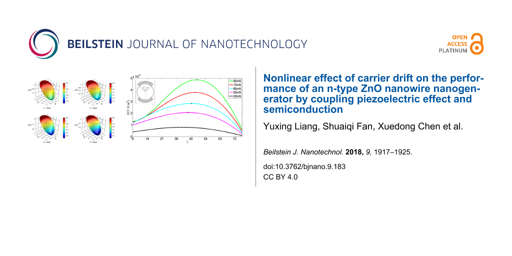
Consider the electrode configuration in the inset of Figure 8. We repeat the numerical calculation by dividing the boundary into two parts: one is the continuous boundary (outside the electrodes) and the other is constant electric potential boundary (inside the electrodes). In this situation, the electric charge Qe at the electrode can be obtained [42,43] through the integral of the boundary electric displacement Dr over the distributed surface 3π/2 − γ < θ < 3π/2 + γ,
![[2190-4286-9-183-i12]](/bjnano/content/inline/2190-4286-9-183-i12.svg?max-width=590&scale=1.18182)
The current flowing through this electrode is ![[Graphic 47]](/bjnano/content/inline/2190-4286-9-183-i60.svg?max-width=637&scale=1.18182) , which indicates that the output current Ie for a harmonic vibration is directly proportional to the amplitude of the boundary electric charge Qe. Thus, for convenience we define the quantity W,
, which indicates that the output current Ie for a harmonic vibration is directly proportional to the amplitude of the boundary electric charge Qe. Thus, for convenience we define the quantity W,
![[2190-4286-9-183-i13]](/bjnano/content/inline/2190-4286-9-183-i13.svg?max-width=590&scale=1.18182)
which is directly proportional to the output power of the ZNW generator. ![[Graphic 48]](/bjnano/content/inline/2190-4286-9-183-i61.svg?max-width=637&scale=1.18182) stands for the electric potential difference between the two electrodes and θ0 = γ + 3π/2. Figure 8 shows W as a function of
stands for the electric potential difference between the two electrodes and θ0 = γ + 3π/2. Figure 8 shows W as a function of ![[Graphic 49]](/bjnano/content/inline/2190-4286-9-183-i62.svg?max-width=637&scale=1.18182) , with
, with ![[Graphic 50]](/bjnano/content/inline/2190-4286-9-183-i63.svg?max-width=637&scale=1.18182) . With P changing from 30 to 80 nN, the peak point of W moves from θ0 = 1.72π (
. With P changing from 30 to 80 nN, the peak point of W moves from θ0 = 1.72π (![[Graphic 51]](/bjnano/content/inline/2190-4286-9-183-i64.svg?max-width=637&scale=1.18182) ≈ 40°) to θ0 = 1.77π (
≈ 40°) to θ0 = 1.77π (![[Graphic 52]](/bjnano/content/inline/2190-4286-9-183-i65.svg?max-width=637&scale=1.18182) ≈ 49°). Obviously, a flare angle of 2
≈ 49°). Obviously, a flare angle of 2![[Graphic 53]](/bjnano/content/inline/2190-4286-9-183-i66.svg?max-width=637&scale=1.18182) ≈ 98° of the two electrodes is suitable for all loadings below 80 nN. This electrode configuration provides an optimal output of the nanogenerator.
≈ 98° of the two electrodes is suitable for all loadings below 80 nN. This electrode configuration provides an optimal output of the nanogenerator.
![[2190-4286-9-183-8]](/bjnano/content/figures/2190-4286-9-183-8.png?scale=2.0&max-width=1024&background=FFFFFF)
Figure 8: W as a function of the electrode configuration for different end forces.
Figure 8: W as a function of the electrode configuration for different end forces.
In addition, we show the effect of the initial carrier concentration on the optimal electrode configuration in Figure 9 for n0 = 1·1022, 1·1023 and 1·1024 m−3. Obviously, a smaller initial carrier concentration is corresponding to a higher energy harvest. It is readily understood that semiconduction results in some electric leakage, and thus reduces the output power. For different initial carrier concentrations, electrode configurations with flare angles of 2![[Graphic 54]](/bjnano/content/inline/2190-4286-9-183-i67.svg?max-width=637&scale=1.18182) ≈ 88°, 98° and 88° are suitable for a ZNW generator with n0 = 1·1022, 1·1023 and 1·1024 m−3, respectively.
≈ 88°, 98° and 88° are suitable for a ZNW generator with n0 = 1·1022, 1·1023 and 1·1024 m−3, respectively.
![[2190-4286-9-183-9]](/bjnano/content/figures/2190-4286-9-183-9.png?scale=2.0&max-width=1024&background=FFFFFF)
Figure 9: W as a function of the electrode configuration for different initial carrier concentrations.
Figure 9: W as a function of the electrode configuration for different initial carrier concentrations.
Conclusion
Nonlinear solutions for carrier concentration, electric field and electric potential in a bent ZNW are obtained without the assumption of small fluctuations of carrier concentration. As the bending deformation increases, carriers are gradually accumulated in the stretched portion of the ZNW, and the boundary charge is greatly increased. It is found that the electrode configuration will have a large influence on the output performance of a bent ZNW generator. Thus it is of significance to design an electrode configuration for an optimal output. Both the analysis technique and the obtained results are useful in the design of piezotronics and piezo-phototropic devices and the corresponding applications.
Acknowledgements
This work was supported by the National Natural Science Foundation of China (Grant Nos. 11672113 and 51435006) and the Key Laboratory Project of Hubei Province (No. 2016CFA073). Many thanks to Professor Yunbo Wang at School of Optical and Electronic Information of Huazhong University of Science and Technology for the helpful discussions and suggestions.
References
-
Hutson, A. R.; White, D. L. J. Appl. Phys. 1962, 33, 40–47. doi:10.1063/1.1728525
Return to citation in text: [1] -
White, D. L. J. Appl. Phys. 1962, 33, 2547–2554. doi:10.1063/1.1729015
Return to citation in text: [1] -
Collins, J. H.; Lakin, K. M.; Quate, C. F.; Shaw, H. J. Appl. Phys. Lett. 1968, 13, 314–316. doi:10.1063/1.1652628
Return to citation in text: [1] -
Yang, J. S.; Zhou, H. G. Int. J. Solids Struct. 2005, 42, 3171–3183. doi:10.1016/j.ijsolstr.2004.10.011
Return to citation in text: [1] [2] -
Weinreich, G.; Sanders, T. M., Jr.; White, H. G. Phys. Rev. 1959, 114, 33–44. doi:10.1103/PhysRev.114.33
Return to citation in text: [1] -
Zhang, Y.; Liu, Y.; Wang, Z. L. Adv. Mater. 2011, 23, 3004–3013. doi:10.1002/adma.201100906
Return to citation in text: [1] -
Dahiya, R. S.; Metta, G.; Valle, M.; Adami, A.; Lorenzelli, L. Appl. Phys. Lett. 2009, 95, 034105. doi:10.1063/1.3184579
Return to citation in text: [1] -
Wu, Y.-R.; Singh, J. Appl. Phys. Lett. 2004, 85, 1223–1225. doi:10.1063/1.1784039
Return to citation in text: [1] -
Wu, W.; Pan, C.; Zhang, Y.; Wen, X.; Wang, Z. L. Nano Today 2013, 8, 619–642. doi:10.1016/j.nantod.2013.11.002
Return to citation in text: [1] -
Wang, Z. L. Mater. Sci. Eng., R 2009, 64, 33–71. doi:10.1016/j.mser.2009.02.001
Return to citation in text: [1] -
Mante, P.-A.; Huang, Y.-R.; Yang, S.-C.; Liu, T.-M.; Maznev, A. A.; Sheu, J.-K.; Sun, C.-K. Ultrasonics 2015, 56, 52–65. doi:10.1016/j.ultras.2014.09.020
Return to citation in text: [1] -
Willatzen, M.; Christensen, J. Phys. Rev. B 2014, 89, 041201. doi:10.1103/PhysRevB.89.041201
Return to citation in text: [1] -
Gokhale, V. J.; Rais-Zadeh, M. Sci. Rep. 2014, 4, 5617. doi:10.1038/srep05617
Return to citation in text: [1] -
Trotta, R.; Wildmann, J. S.; Zallo, E.; Schmidt, O. G.; Rastelli, A. Nano Lett. 2014, 14, 3439–3444. doi:10.1021/nl500968k
Return to citation in text: [1] -
Yakovenko, V. M. Physica B 2012, 407, 1969–1972. doi:10.1016/j.physb.2012.01.076
Return to citation in text: [1] -
Fan, L.; Chen, Z.; Zhang, S.-y.; Zhang, H. J. Appl. Phys. 2014, 115, 064506. doi:10.1063/1.4865172
Return to citation in text: [1] -
Shim, Y.-S.; Zhang, L.; Kim, D. H.; Kim, Y. H.; Choi, Y. R.; Nahm, S. H.; Kang, C.-Y.; Lee, W.; Jang, H. W. Sens. Actuators, B 2014, 198, 294–301. doi:10.1016/j.snb.2014.03.073
Return to citation in text: [1] -
Qin, Y.; Wang, X.; Wang, Z. L. Nature 2008, 451, 809–813. doi:10.1038/nature06601
Return to citation in text: [1] -
Yang, R. S.; Qin, Y.; Dai, L.; Wang, Z. L. Nat. Nanotechnol. 2009, 4, 34–39. doi:10.1038/nnano.2008.314
Return to citation in text: [1] -
Xu, S.; Qin, Y.; Xu, C.; Wei, Y.; Yang, R.; Wang, Z. L. Nat. Nanotechnol. 2010, 5, 366–373. doi:10.1038/nnano.2010.46
Return to citation in text: [1] -
Zhu, G.; Yang, R.; Wang, S.; Wang, Z. L. Nano Lett. 2010, 10, 3151–3155. doi:10.1021/nl101973h
Return to citation in text: [1] -
Wang, Z. L. Adv. Funct. Mater. 2008, 18, 3553–3567. doi:10.1002/adfm.200800541
Return to citation in text: [1] -
Wang, Z. L.; Yang, R.; Zhou, J.; Qin, Y.; Xu, C.; Hu, Y.; Xu, S. Mater. Sci. Eng., R 2010, 70, 320–329. doi:10.1016/j.mser.2010.06.015
Return to citation in text: [1] -
Wang, Z. L. Nanogenerators for Self-powered Devices and Systems; Georgia Institute of Technology: Atlanta, GA, U.S.A., 2011.
https://smartech.gatech.edu/handle/1853/39262
Return to citation in text: [1] -
Wang, Z. L. Physics (China) 2006, 35, 897–903.
Return to citation in text: [1] -
Gao, Y.; Wang, Z. L. Nano Lett. 2007, 7, 2499–2505. doi:10.1021/nl071310j
Return to citation in text: [1] [2] [3] -
Gao, Y.; Wang, Z. L. Nano Lett. 2009, 9, 1103–1110. doi:10.1021/nl803547f
Return to citation in text: [1] [2] [3] [4] -
Wang, Z. L.; Song, J. Science 2006, 312, 242–246. doi:10.1126/science.1124005
Return to citation in text: [1] [2] -
Sun, C.; Shi, J.; Wang, X. J. Appl. Phys. 2010, 108, 034309. doi:10.1063/1.3462468
Return to citation in text: [1] [2] -
Wang, Z. L. Piezotronics and Piezo-Phototronics; Springer: Berlin, Germany, 2012. doi:10.1007/978-3-642-34237-0
Return to citation in text: [1] [2] [3] [4] [5] -
Fan, S.; Liang, Y.; Xie, J.; Hu, Y. Nano Energy 2017, 40, 82–87. doi:10.1016/j.nanoen.2017.07.049
Return to citation in text: [1] [2] [3] [4] [5] [6] [7] -
Xie, J.; Yang, J.; Hu, H.; Hu, Y.; Chen, X. J. Intell. Mater. Syst. Struct. 2012, 23, 135–139. doi:10.1177/1045389X11431744
Return to citation in text: [1] -
Wang, H.-r.; Xie, J.-m.; Xie, X.; Hu, Y.-t.; Wang, J. Appl. Math. Mech. (Engl. Ed.) 2014, 35, 229–236. doi:10.1007/s10483-014-1786-6
Return to citation in text: [1] -
Henneghien, A.-L.; Gayral, B.; Désières, Y.; Gérard, J.-M. J. Opt. Soc. Am. B 2009, 26, 2396–2403. doi:10.1364/JOSAB.26.002396
Return to citation in text: [1] -
Maslov, A. V.; Bakunov, M. I.; Ning, C. Z. J. Appl. Phys. 2006, 99, 024314. doi:10.1063/1.2164538
Return to citation in text: [1] -
Yang, J. An Introduction to the Theory of Piezoelectricity; Springer: New York, NY, U.S.A., 2005. doi:10.1007/b101799
Return to citation in text: [1] -
Kobiakov, I. B. Solid State Commun. 1980, 35, 305–310. doi:10.1016/0038-1098(80)90502-5
Return to citation in text: [1] -
Carlotti, G.; Socino, G.; Petri, A.; Verona, E. Appl. Phys. Lett. 1987, 51, 1889–1891. doi:10.1063/1.98502
Return to citation in text: [1] -
Zhang, C.; Wang, X.; Chen, W.; Yang, J. Smart Mater. Struct. 2017, 26, 025030. doi:10.1088/1361-665X/aa542e
Return to citation in text: [1] -
Hu, Y.; Zeng, Y.; Yang, J. Int. J. Solids Struct. 2007, 44, 3928–3938. doi:10.1016/j.ijsolstr.2006.10.033
Return to citation in text: [1] -
Luo, Y.; Cheng, R.; Zhang, C.; Chen, W.; Yang, J. Acta Mech. Solida Sin. 2018, 31, 127–140. doi:10.1007/s10338-018-0010-1
Return to citation in text: [1] -
Yang, J. S.; Fang, H. Y. IEEE Trans. Ultrason., Ferroelectr., Freq. Control 2002, 49, 798–804. doi:10.1109/TUFFC.2002.1009338
Return to citation in text: [1] -
Yang, J. Acta Mech. Solida Sin. 2017, 30, 21–26. doi:10.1016/j.camss.2016.05.001
Return to citation in text: [1]
| 26. | Gao, Y.; Wang, Z. L. Nano Lett. 2007, 7, 2499–2505. doi:10.1021/nl071310j |
| 27. | Gao, Y.; Wang, Z. L. Nano Lett. 2009, 9, 1103–1110. doi:10.1021/nl803547f |
| 28. | Wang, Z. L.; Song, J. Science 2006, 312, 242–246. doi:10.1126/science.1124005 |
| 29. | Sun, C.; Shi, J.; Wang, X. J. Appl. Phys. 2010, 108, 034309. doi:10.1063/1.3462468 |
| 30. | Wang, Z. L. Piezotronics and Piezo-Phototronics; Springer: Berlin, Germany, 2012. doi:10.1007/978-3-642-34237-0 |
| 31. | Fan, S.; Liang, Y.; Xie, J.; Hu, Y. Nano Energy 2017, 40, 82–87. doi:10.1016/j.nanoen.2017.07.049 |
| 31. | Fan, S.; Liang, Y.; Xie, J.; Hu, Y. Nano Energy 2017, 40, 82–87. doi:10.1016/j.nanoen.2017.07.049 |
| 36. | Yang, J. An Introduction to the Theory of Piezoelectricity; Springer: New York, NY, U.S.A., 2005. doi:10.1007/b101799 |
| 37. | Kobiakov, I. B. Solid State Commun. 1980, 35, 305–310. doi:10.1016/0038-1098(80)90502-5 |
| 38. | Carlotti, G.; Socino, G.; Petri, A.; Verona, E. Appl. Phys. Lett. 1987, 51, 1889–1891. doi:10.1063/1.98502 |
| 39. | Zhang, C.; Wang, X.; Chen, W.; Yang, J. Smart Mater. Struct. 2017, 26, 025030. doi:10.1088/1361-665X/aa542e |
| 40. | Hu, Y.; Zeng, Y.; Yang, J. Int. J. Solids Struct. 2007, 44, 3928–3938. doi:10.1016/j.ijsolstr.2006.10.033 |
| 41. | Luo, Y.; Cheng, R.; Zhang, C.; Chen, W.; Yang, J. Acta Mech. Solida Sin. 2018, 31, 127–140. doi:10.1007/s10338-018-0010-1 |
| 1. | Hutson, A. R.; White, D. L. J. Appl. Phys. 1962, 33, 40–47. doi:10.1063/1.1728525 |
| 2. | White, D. L. J. Appl. Phys. 1962, 33, 2547–2554. doi:10.1063/1.1729015 |
| 3. | Collins, J. H.; Lakin, K. M.; Quate, C. F.; Shaw, H. J. Appl. Phys. Lett. 1968, 13, 314–316. doi:10.1063/1.1652628 |
| 4. | Yang, J. S.; Zhou, H. G. Int. J. Solids Struct. 2005, 42, 3171–3183. doi:10.1016/j.ijsolstr.2004.10.011 |
| 16. | Fan, L.; Chen, Z.; Zhang, S.-y.; Zhang, H. J. Appl. Phys. 2014, 115, 064506. doi:10.1063/1.4865172 |
| 17. | Shim, Y.-S.; Zhang, L.; Kim, D. H.; Kim, Y. H.; Choi, Y. R.; Nahm, S. H.; Kang, C.-Y.; Lee, W.; Jang, H. W. Sens. Actuators, B 2014, 198, 294–301. doi:10.1016/j.snb.2014.03.073 |
| 34. | Henneghien, A.-L.; Gayral, B.; Désières, Y.; Gérard, J.-M. J. Opt. Soc. Am. B 2009, 26, 2396–2403. doi:10.1364/JOSAB.26.002396 |
| 12. | Willatzen, M.; Christensen, J. Phys. Rev. B 2014, 89, 041201. doi:10.1103/PhysRevB.89.041201 |
| 13. | Gokhale, V. J.; Rais-Zadeh, M. Sci. Rep. 2014, 4, 5617. doi:10.1038/srep05617 |
| 14. | Trotta, R.; Wildmann, J. S.; Zallo, E.; Schmidt, O. G.; Rastelli, A. Nano Lett. 2014, 14, 3439–3444. doi:10.1021/nl500968k |
| 15. | Yakovenko, V. M. Physica B 2012, 407, 1969–1972. doi:10.1016/j.physb.2012.01.076 |
| 35. | Maslov, A. V.; Bakunov, M. I.; Ning, C. Z. J. Appl. Phys. 2006, 99, 024314. doi:10.1063/1.2164538 |
| 6. | Zhang, Y.; Liu, Y.; Wang, Z. L. Adv. Mater. 2011, 23, 3004–3013. doi:10.1002/adma.201100906 |
| 7. | Dahiya, R. S.; Metta, G.; Valle, M.; Adami, A.; Lorenzelli, L. Appl. Phys. Lett. 2009, 95, 034105. doi:10.1063/1.3184579 |
| 8. | Wu, Y.-R.; Singh, J. Appl. Phys. Lett. 2004, 85, 1223–1225. doi:10.1063/1.1784039 |
| 9. | Wu, W.; Pan, C.; Zhang, Y.; Wen, X.; Wang, Z. L. Nano Today 2013, 8, 619–642. doi:10.1016/j.nantod.2013.11.002 |
| 10. | Wang, Z. L. Mater. Sci. Eng., R 2009, 64, 33–71. doi:10.1016/j.mser.2009.02.001 |
| 11. | Mante, P.-A.; Huang, Y.-R.; Yang, S.-C.; Liu, T.-M.; Maznev, A. A.; Sheu, J.-K.; Sun, C.-K. Ultrasonics 2015, 56, 52–65. doi:10.1016/j.ultras.2014.09.020 |
| 31. | Fan, S.; Liang, Y.; Xie, J.; Hu, Y. Nano Energy 2017, 40, 82–87. doi:10.1016/j.nanoen.2017.07.049 |
| 42. | Yang, J. S.; Fang, H. Y. IEEE Trans. Ultrason., Ferroelectr., Freq. Control 2002, 49, 798–804. doi:10.1109/TUFFC.2002.1009338 |
| 43. | Yang, J. Acta Mech. Solida Sin. 2017, 30, 21–26. doi:10.1016/j.camss.2016.05.001 |
| 4. | Yang, J. S.; Zhou, H. G. Int. J. Solids Struct. 2005, 42, 3171–3183. doi:10.1016/j.ijsolstr.2004.10.011 |
| 5. | Weinreich, G.; Sanders, T. M., Jr.; White, H. G. Phys. Rev. 1959, 114, 33–44. doi:10.1103/PhysRev.114.33 |
| 26. | Gao, Y.; Wang, Z. L. Nano Lett. 2007, 7, 2499–2505. doi:10.1021/nl071310j |
| 27. | Gao, Y.; Wang, Z. L. Nano Lett. 2009, 9, 1103–1110. doi:10.1021/nl803547f |
| 31. | Fan, S.; Liang, Y.; Xie, J.; Hu, Y. Nano Energy 2017, 40, 82–87. doi:10.1016/j.nanoen.2017.07.049 |
| 30. | Wang, Z. L. Piezotronics and Piezo-Phototronics; Springer: Berlin, Germany, 2012. doi:10.1007/978-3-642-34237-0 |
| 30. | Wang, Z. L. Piezotronics and Piezo-Phototronics; Springer: Berlin, Germany, 2012. doi:10.1007/978-3-642-34237-0 |
| 30. | Wang, Z. L. Piezotronics and Piezo-Phototronics; Springer: Berlin, Germany, 2012. doi:10.1007/978-3-642-34237-0 |
| 30. | Wang, Z. L. Piezotronics and Piezo-Phototronics; Springer: Berlin, Germany, 2012. doi:10.1007/978-3-642-34237-0 |
| 32. | Xie, J.; Yang, J.; Hu, H.; Hu, Y.; Chen, X. J. Intell. Mater. Syst. Struct. 2012, 23, 135–139. doi:10.1177/1045389X11431744 |
| 33. | Wang, H.-r.; Xie, J.-m.; Xie, X.; Hu, Y.-t.; Wang, J. Appl. Math. Mech. (Engl. Ed.) 2014, 35, 229–236. doi:10.1007/s10483-014-1786-6 |
| 31. | Fan, S.; Liang, Y.; Xie, J.; Hu, Y. Nano Energy 2017, 40, 82–87. doi:10.1016/j.nanoen.2017.07.049 |
| 28. | Wang, Z. L.; Song, J. Science 2006, 312, 242–246. doi:10.1126/science.1124005 |
| 29. | Sun, C.; Shi, J.; Wang, X. J. Appl. Phys. 2010, 108, 034309. doi:10.1063/1.3462468 |
| 31. | Fan, S.; Liang, Y.; Xie, J.; Hu, Y. Nano Energy 2017, 40, 82–87. doi:10.1016/j.nanoen.2017.07.049 |
| 18. | Qin, Y.; Wang, X.; Wang, Z. L. Nature 2008, 451, 809–813. doi:10.1038/nature06601 |
| 19. | Yang, R. S.; Qin, Y.; Dai, L.; Wang, Z. L. Nat. Nanotechnol. 2009, 4, 34–39. doi:10.1038/nnano.2008.314 |
| 20. | Xu, S.; Qin, Y.; Xu, C.; Wei, Y.; Yang, R.; Wang, Z. L. Nat. Nanotechnol. 2010, 5, 366–373. doi:10.1038/nnano.2010.46 |
| 21. | Zhu, G.; Yang, R.; Wang, S.; Wang, Z. L. Nano Lett. 2010, 10, 3151–3155. doi:10.1021/nl101973h |
| 22. | Wang, Z. L. Adv. Funct. Mater. 2008, 18, 3553–3567. doi:10.1002/adfm.200800541 |
| 23. | Wang, Z. L.; Yang, R.; Zhou, J.; Qin, Y.; Xu, C.; Hu, Y.; Xu, S. Mater. Sci. Eng., R 2010, 70, 320–329. doi:10.1016/j.mser.2010.06.015 |
| 24. |
Wang, Z. L. Nanogenerators for Self-powered Devices and Systems; Georgia Institute of Technology: Atlanta, GA, U.S.A., 2011.
https://smartech.gatech.edu/handle/1853/39262 |
| 25. | Wang, Z. L. Physics (China) 2006, 35, 897–903. |
| 26. | Gao, Y.; Wang, Z. L. Nano Lett. 2007, 7, 2499–2505. doi:10.1021/nl071310j |
| 27. | Gao, Y.; Wang, Z. L. Nano Lett. 2009, 9, 1103–1110. doi:10.1021/nl803547f |
| 31. | Fan, S.; Liang, Y.; Xie, J.; Hu, Y. Nano Energy 2017, 40, 82–87. doi:10.1016/j.nanoen.2017.07.049 |
© 2018 Liang et al.; licensee Beilstein-Institut.
This is an Open Access article under the terms of the Creative Commons Attribution License (http://creativecommons.org/licenses/by/4.0), which permits unrestricted use, distribution, and reproduction in any medium, provided the original work is properly cited.
The license is subject to the Beilstein Journal of Nanotechnology terms and conditions: (https://www.beilstein-journals.org/bjnano)