Supporting Information
| Supporting Information File 1: Additional experimental data. | ||
| Format: PDF | Size: 1.5 MB | Download |
Cite the Following Article
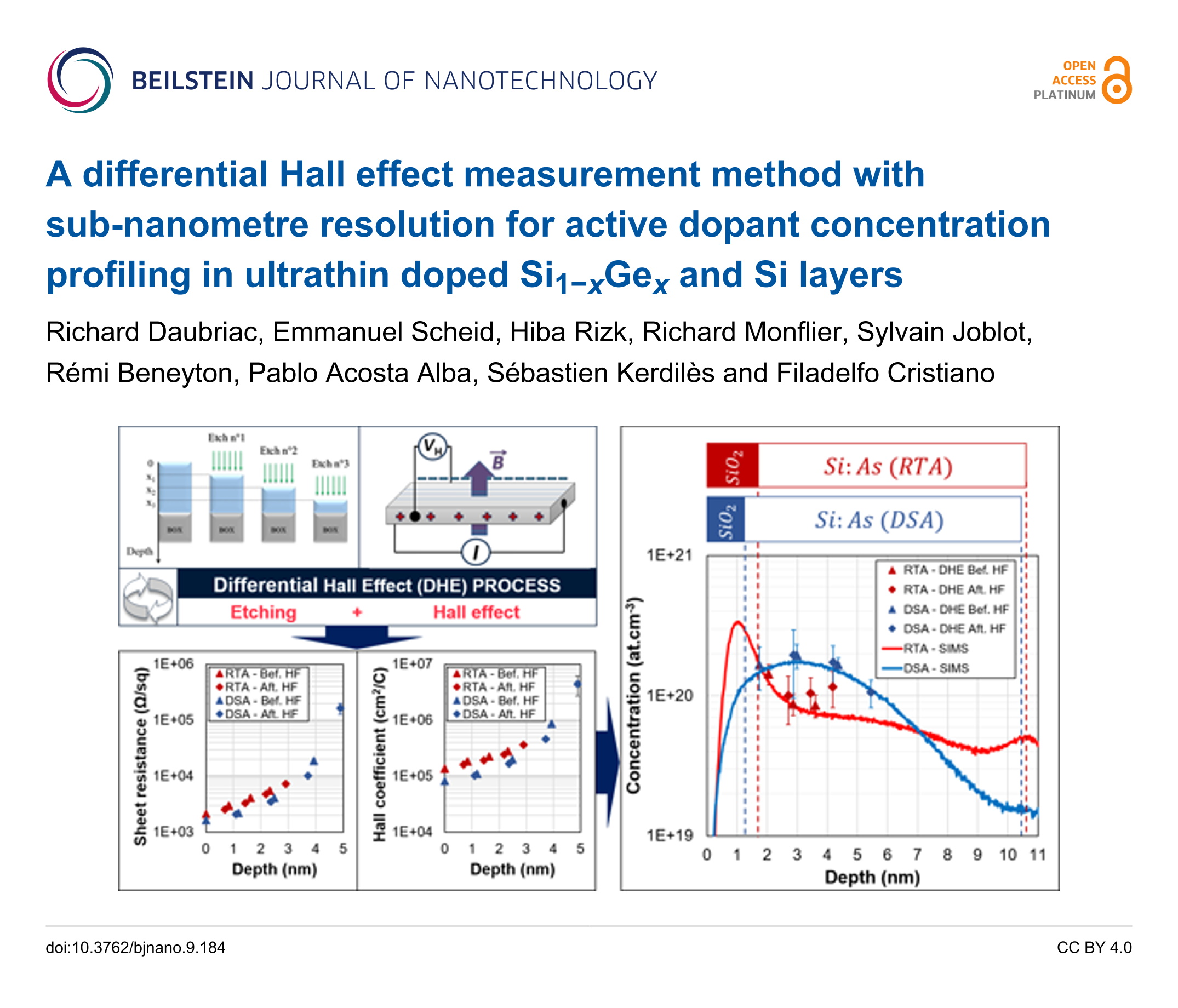
A differential Hall effect measurement method with sub-nanometre resolution for active dopant concentration profiling in ultrathin doped Si1−xGex and Si layers
Richard Daubriac, Emmanuel Scheid, Hiba Rizk, Richard Monflier, Sylvain Joblot, Rémi Beneyton, Pablo Acosta Alba, Sébastien Kerdilès and Filadelfo Cristiano
Beilstein J. Nanotechnol. 2018, 9, 1926–1939.
https://doi.org/10.3762/bjnano.9.184
How to Cite
Daubriac, R.; Scheid, E.; Rizk, H.; Monflier, R.; Joblot, S.; Beneyton, R.; Acosta Alba, P.; Kerdilès, S.; Cristiano, F. Beilstein J. Nanotechnol. 2018, 9, 1926–1939. doi:10.3762/bjnano.9.184
Download Citation
Citation data can be downloaded as file using the "Download" button or used for copy/paste from the text window
below.
Citation data in RIS format can be imported by all major citation management software, including EndNote,
ProCite, RefWorks, and Zotero.
Presentation Graphic
| Picture with graphical abstract, title and authors for social media postings and presentations. | ||
| Format: PNG | Size: 843.3 KB | Download |
Citations to This Article
Up to 20 of the most recent references are displayed here.
Scholarly Works
- Dong, K.; Mei, D.; Panamaldeniya, S. A.; Karki, A.; Burns, P.; Bhattarai, S. Hybrid-contact planar HPGe process vehicle toward ring-contact designs. Journal of Instrumentation 2026, 21, P04023. doi:10.1088/1748-0221/21/04/p04023
- Jo, C.; Ko, D.-H. Deactivation phenomena of highly B-doped SiGe epitaxial films subjected to nanosecond laser annealing followed by rapid thermal annealing. Surfaces and Interfaces 2026, 84, 108589. doi:10.1016/j.surfin.2026.108589
- Román-Sánchez, S.; Moure, A.; López-Sánchez, J.; Rubio-Zuazo, J.; del Campo, A.; Oujja, M.; Calvo, R.; Sánchez-Prieto, J.; Lorite, I.; Fernández, J. F.; Serrano, A. In-Operando local structural response of Si-based press-fit PN-junction diodes. Results in Engineering 2026, 29, 109669. doi:10.1016/j.rineng.2026.109669
- Kerdilès, S.; Opprecht, M.; Bosch, D.; Ribotta, M.; Sklénard, B.; Brunet, L.; Michalowski, P. Solid-phase epitaxial regrowth of phosphorus-doped silicon by nanosecond laser annealing. Materials Science in Semiconductor Processing 2025, 186, 109043. doi:10.1016/j.mssp.2024.109043
- Cabaret, T.; Dos Reis, E.; Lapras, V.; Gauthier, N.; Kanyandekwe, J. Diffusion Analysis and Impact of RTA on Strained Phosphorous-Doped Si for Advanced SOI Nodes. IEEE Journal of the Electron Devices Society 2025, 13, 1306–1312. doi:10.1109/jeds.2025.3642939
- Basol, B. M.; Joshi, A. Differential Hall Effect Metrology for Electrical Characterization of Advanced Semiconductor Layers. Metrology 2024, 4, 547–565. doi:10.3390/metrology4040034
- Jo, C.; Lee, K.; Yoon, D.; Ko, D.-H. Strain behavior and dopant activation of heavily in-situ B-doped SiGe epitaxial films treated by nanosecond laser annealing. Materials Science in Semiconductor Processing 2024, 175, 108215. doi:10.1016/j.mssp.2024.108215
- Ibrahim, I. M.; Noori, Z. M.; Hwail, H. M.; Abdullah, M. M. Morphological and Optical Study of Black P- Silicon Textured in KOH Bath. Diffusion Foundations and Materials Applications 2023, 32, 35–43. doi:10.4028/p-94981s
- Alberti, A.; Giannazzo, F.; Via, F. L.; Lombardo, S.; Mio, A. M.; Nicotra, G.; Privitera, S. M. S.; Reitano, R.; Roccaforte, F.; Spinella, C.; Rimini, E. Measuring Techniques for the Semiconductor's Parameters. Springer Handbooks; Springer International Publishing, 2022; pp 117–168. doi:10.1007/978-3-030-79827-7_4
- Wójcik, A.; Kolkowski, W.; Pasternak, I.; Strupinski, W.; Kozdra, S.; Michałowski, P. P. Electrically active and hydrogen passivated Zn in GaAs/AlGaAs specifically distinguished during secondary ion mass spectrometry depth profiling. Journal of Analytical Atomic Spectrometry 2021, 36, 178–184. doi:10.1039/d0ja00369g