Supporting Information
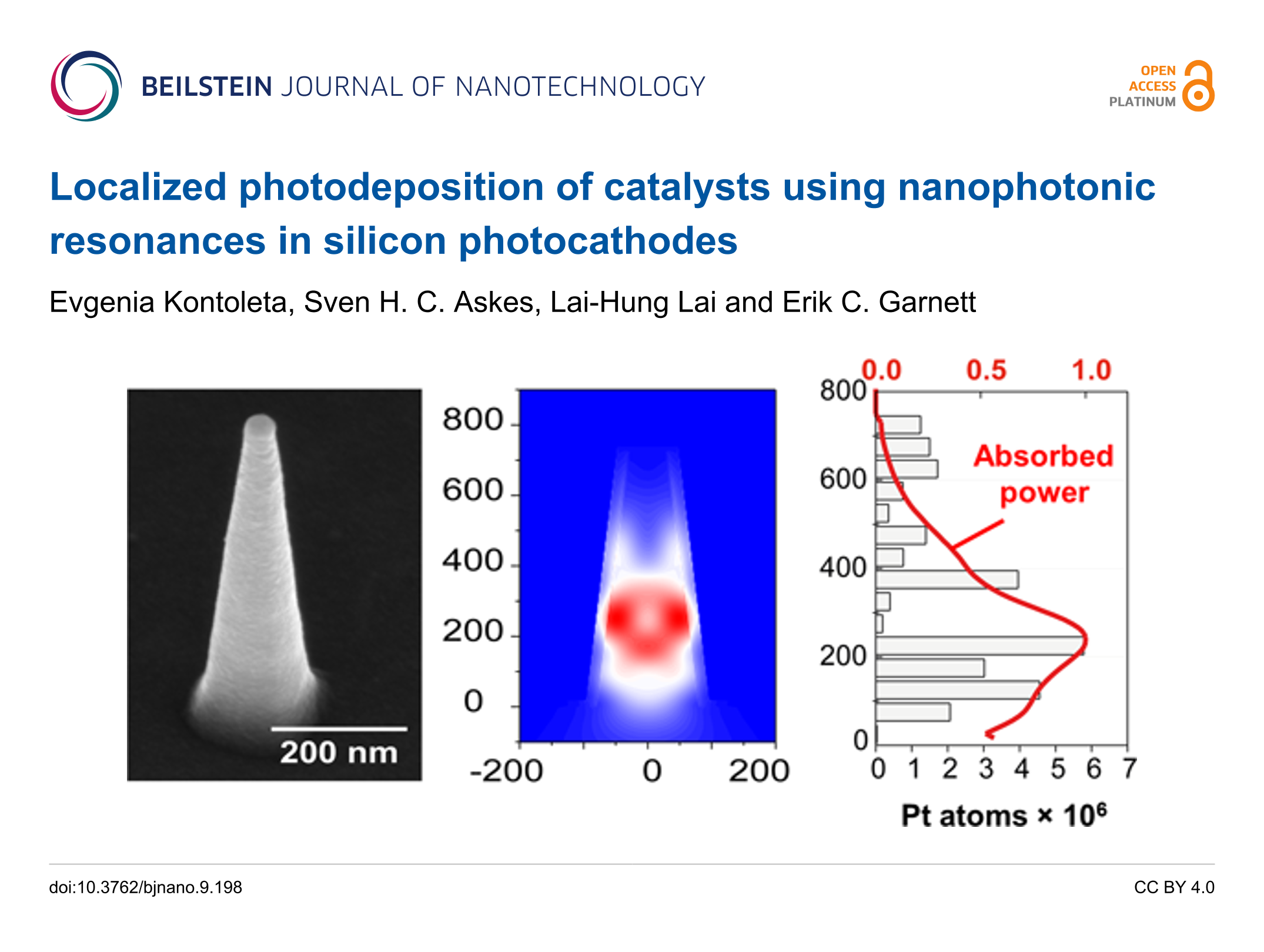
Schematic description of the experimental process step by step for the Si nanostructures fabrication; XRD and ellipsometry data of the TiO2 layer; chronoamperometry measurements of Si nanocones with and without TiO2 layer; SEM image of Si nanocone after illumination without the TiO2 layer; current-vs-potential measurement on silicon nanocones; SEM images in and out of the illumination spot and of the illumination spot itself; representation of the photo-electrochemical cell; schematic diagram of the FDTD simulations and SEM images of more silicon nanostructures after photo-electrodeposition of platinum for verification of the effect.
| Supporting Information File 1: Additional experimental data. | ||
| Format: PDF | Size: 1.5 MB | Download |
Cite the Following Article
How to Cite
Download Citation
Citation data can be downloaded as file using the "Download" button or used for copy/paste from the text window
below.
Citation data in RIS format can be imported by all major citation management software, including EndNote,
ProCite, RefWorks, and Zotero.
Presentation Graphic
| Picture with graphical abstract, title and authors for social media postings and presentations. | ||
| Format: PNG | Size: 598.9 KB | Download |
Citations to This Article
Scholarly Works
- Yuan, X.; Wang, S.; Gu, L.; Xie, S.; Ma, Q.; Guo, J. Multi-headed tandem neural network approach for non-uniqueness in inverse design of layered photonic structures. Optics & Laser Technology 2024, 176, 110997. doi:10.1016/j.optlastec.2024.110997
- Mönig, H.; Schmid, M. Renewable energy conversion using nano- and microstructured materials. Beilstein journal of nanotechnology 2019, 10, 771–773. doi:10.3762/bjnano.10.76