This search combines search strings from the content search (i.e. "Full Text", "Author", "Title", "Abstract", or "Keywords") with "Article Type" and "Publication Date Range" using the AND operator.
Beilstein J. Nanotechnol. 2026, 17, 796–805, doi:10.3762/bjnano.17.56
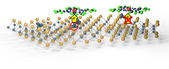
Figure 1: ARPES band structure of MoS2 before (a–c) and after sputtering (d–f) and the subsequent deposition ...
Figure 2: Co L2,3 XAS spectra of CoPcF16 coverages in the mono- or multilayer range on Ne+ or Ar+ sputtered M...
Figure 3: Co 2p XPS spectra before and after the deposition of mono- and multilayer films of CoPcF16 after (a...
Figure 4: Molecule-related C 1s (a,b,c) and N 1s (d,e,f) core level spectra on differently sputtered MoS2 sur...
Figure 5: XPS measurements of the Mo 3d core levels of MoS2 following the sputtering with Ar+ and Ne+ and the...
Beilstein J. Nanotechnol. 2026, 17, 505–514, doi:10.3762/bjnano.17.33
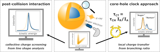
Figure 1: S KL2,3L2,3 resonant Auger measurements of core–shell nanoparticles (core: 3.5 nm CdSe, shell: 7 do...
Figure 2: Charge transfer times of the core–shell nanoparticles (CdSe core diameter 3.5 nm) with different Zn...
Figure 3: Post-collision interaction (PCI) between Auger and photoelectron interacting within the internal sc...
Figure 4: Size-dependence of the PCI asymmetry parameter. Top panel: Asymmetry parameter ξ for nanoparticles ...
Figure 5: Variation of internal charge transfer continuum coupling as seen by the PCI parameter as a function...