


Search results
Search for "sub-nanometre resolution" in Full Text gives 3 result(s) in Beilstein Journal of Nanotechnology.
He+ FIBID-fabricated 3D AFM tip architectures: an exploratory study of hollow pillars, helices, and spirals
Beilstein J. Nanotechnol. 2026, 17, 863–871, doi:10.3762/bjnano.17.62
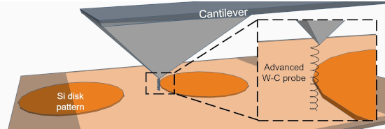
- versatile technique for nanoscale surface characterisation that enables topographic measurements with sub-nanometre resolution by means of a sharp tip mounted at the end of a flexible cantilever [1]. During operation, the tip scans across the sample surface and responds to local interactions such as van der


Bio-imaging with the helium-ion microscope: A review
Beilstein J. Nanotechnol. 2021, 12, 1–23, doi:10.3762/bjnano.12.1
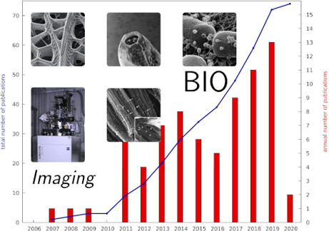
- of Physics, University of Jyväskylä, P.O. Box 35, FI-40014 Jyväskylä, Finland 10.3762/bjnano.12.1 Abstract Scanning helium-ion microscopy (HIM) is an imaging technique with sub-nanometre resolution and is a powerful tool to resolve some of the tiniest structures in biology. In many aspects, the HIM


A differential Hall effect measurement method with sub-nanometre resolution for active dopant concentration profiling in ultrathin doped Si1−xGex and Si layers
Beilstein J. Nanotechnol. 2018, 9, 1926–1939, doi:10.3762/bjnano.9.184
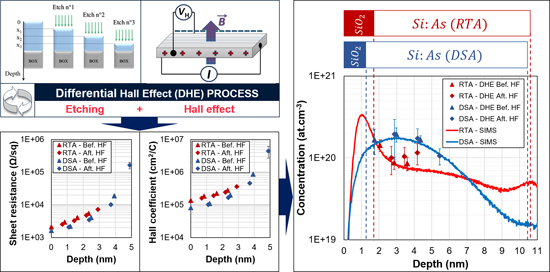
- Grenoble, France 10.3762/bjnano.9.184 Abstract In this paper, we present an enhanced differential Hall effect measurement method (DHE) for ultrathin Si and SiGe layers for the investigation of dopant activation in the surface region with sub-nanometre resolution. In the case of SiGe, which constitutes the
- SiGeOI and 11 nm thick SOI. In both cases, DHE is shown to be a uniquely sensitive characterisation technique for a detailed investigation of dopant activation in ultrashallow layers, providing sub-nanometre resolution for both dopant concentration and carrier mobility depth profiles. Keywords: carrier
- mobility; contact resistance; differential Hall effect; dopant activation; fully depleted silicon on insulator (FDSOI); laser annealing; sub-nanometre resolution; Introduction The research efforts made throughout the last decades have made it possible to keep the momentum for a continuous miniaturization


Other Beilstein-Institut Open Science Activities



