High-resolution electrical and chemical characterization of nm-scale organic and inorganic devices

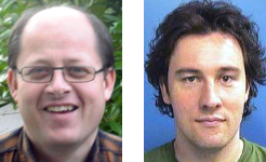
Editors: Prof. Ernst Meyer, Universität Basel
and Dr. Pierre Eyben, IMEC, Leuven
and Dr. Pierre Eyben, IMEC, Leuven
Almost ever since the advent of the microelectronics adventure, silicon-based semiconductor technology has been largely dominant. However, for a few years now this technology has exhibited some fundamental limitations in miniaturization and processing speed and power consumption. Hence, new inorganic semiconductor materials and new architectures are being progressively introduced. The development of high-performance devices is not the only objective of the electronic industry. The need for low-cost devices processed industrially on flexible and light substrates over very large surfaces has led electronic components based on organic semiconductors. The organic materials used nowadays are typically made of single molecules in highly ordered assemblies or of polymeric semiconductors in thin films. It is important to develop and improve two- and threedimensional characterization techniques that can be utilized on both organic and inorganic semiconductors. These techniques should allow nanometer spatial resolution over a broad dynamic range. Ideally, they should also be able to probe the elemental distribution and to provide information on chemical bonding.
High-resolution electrical and chemical characterization of nm-scale organic and inorganic devices
- Pierre Eyben
Beilstein J. Nanotechnol. 2013, 4, 318–319, doi:10.3762/bjnano.4.35

Influence of diffusion on space-charge-limited current measurements in organic semiconductors
- Thomas Kirchartz
Beilstein J. Nanotechnol. 2013, 4, 180–188, doi:10.3762/bjnano.4.18

Photoresponse from single upright-standing ZnO nanorods explored by photoconductive AFM
- Igor Beinik,
- Markus Kratzer,
- Astrid Wachauer,
- Lin Wang,
- Yuri P. Piryatinski,
- Gerhard Brauer,
- Xin Yi Chen,
- Yuk Fan Hsu,
- Aleksandra B. Djurišić and
- Christian Teichert
Beilstein J. Nanotechnol. 2013, 4, 208–217, doi:10.3762/bjnano.4.21

Micro- and nanoscale electrical characterization of large-area graphene transferred to functional substrates
- Gabriele Fisichella,
- Salvatore Di Franco,
- Patrick Fiorenza,
- Raffaella Lo Nigro,
- Fabrizio Roccaforte,
- Cristina Tudisco,
- Guido G. Condorelli,
- Nicolò Piluso,
- Noemi Spartà,
- Stella Lo Verso,
- Corrado Accardi,
- Cristina Tringali,
- Sebastiano Ravesi and
- Filippo Giannazzo
Beilstein J. Nanotechnol. 2013, 4, 234–242, doi:10.3762/bjnano.4.24

A look underneath the SiO2/4H-SiC interface after N2O thermal treatments
- Patrick Fiorenza,
- Filippo Giannazzo,
- Lukas K. Swanson,
- Alessia Frazzetto,
- Simona Lorenti,
- Mario S. Alessandrino and
- Fabrizio Roccaforte
Beilstein J. Nanotechnol. 2013, 4, 249–254, doi:10.3762/bjnano.4.26

Photoelectrochemical and Raman characterization of In2O3 mesoporous films sensitized by CdS nanoparticles
- Mikalai V. Malashchonak,
- Sergey K. Poznyak,
- Eugene A. Streltsov,
- Anatoly I. Kulak,
- Olga V. Korolik and
- Alexander V. Mazanik
Beilstein J. Nanotechnol. 2013, 4, 255–261, doi:10.3762/bjnano.4.27

Molecular dynamics simulations of mechanical failure in polymorphic arrangements of amyloid fibrils containing structural defects
- Hlengisizwe Ndlovu,
- Alison E. Ashcroft,
- Sheena E. Radford and
- Sarah A. Harris
Beilstein J. Nanotechnol. 2013, 4, 429–440, doi:10.3762/bjnano.4.50

Characterization of electroforming-free titanium dioxide memristors
- John Paul Strachan,
- J. Joshua Yang,
- L. A. Montoro,
- C. A. Ospina,
- A. J. Ramirez,
- A. L. D. Kilcoyne,
- Gilberto Medeiros-Ribeiro and
- R. Stanley Williams
Beilstein J. Nanotechnol. 2013, 4, 467–473, doi:10.3762/bjnano.4.55


