Abstract
We report on a wet chemistry method used to grow PtSe2 nanosheets followed by thermal annealing. The SEM and TEM analysis confirms the formation of PtSe2 nanosheets. Furthermore, XRD, Raman, XPS and SAED patterns were used to analyze the crystal structure and to confirm the formation of the PtSe2 phase. The temperature-dependent Raman spectroscopy investigations were carried out on PtSe2 nanosheets deposited on Si substrates in the temperature range 100–506 K. The shifts in Raman active Eg and A1g modes as a function of temperature were monitored. The temperature coefficient for both modes was calculated and was found to match well with the reported 2D transition metal dichalcogenides. A PtSe2 nanosheet-based sensor device was tested for its applicability as a humidity sensor and photodetector. The humidity sensor based on PtSe2 nanosheets showed an excellent recovery time of ≈5 s, indicating the great potential of PtSe2 for future sensor devices.
Introduction
Graphene, the most well-studied example of the two-dimensional (2D) aromatic compounds, is the building block of all forms of carbon allotropes [1]. In recent years, it has been widely studied due to its extraordinary optical, electrical, mechanical, magnetic and chemical properties [2-5]. Like graphene and its organic analogues [6], inorganic 2D metal dichalcogenides also exhibit outstanding performance in many applications including transistors, sensors, photodetectors, solar cells, field emitters, battery materials, light harvesting and energy storage devices, catalyst for H2 generation, and drug delivery applications [7-12]. Most of the transition metal dichalcogenides (TMDCs) are semiconducting in nature with MX2 type – where M is a metal, M = W, Mo, Sn, Nb, V, etc. from group IV–V and X represents the chalcogenides family, X = S, Se, Te, etc. The metal atom M is sandwiched between layers of chalcogenide (X) atoms in the structure X–M–X. The TMDCs show diverse functional properties at the monolayer level in contrast to bulk due to the quantum confinement effect. Apart from this, these TMDCs, for example MoS2 and MoSe2, show an indirect to direct band gap transition [13-17].
A 2D platinum diselenide (PtSe2) material has recently joined the growing class of stable TMDCs due its promising applications. The 2D PtSe2 has not been explored much to date due to difficulties in synthesis. It is well known that bulk PtSe2 is a semimetal in nature with a nearly zero band gap [18,19]. With the help of theoretical calculations such as density functional theory (DFT) and local-density approximations (LDAs), it has been observed that bulk PtSe2 shows a semimetallic nature and single-layer PtSe2 has a semiconducting nature with a bandgap of 1.2 eV. Bilayer PtSe2 is also a semiconducting material but with a slightly smaller band gap than the monolayer material [19]. This layer-dependent conversion of semimetal-to-semiconductor transition has potential for electronic device applications [20-22]. Bulk PtSe2 was first prepared in 1909 by Minozzi from elements [23]. PtSe2 nanosheets have been recently prepared by heating thin foils of platinum in selenium vapors at 400 °C [19,24]. In this paper we have synthesized few-layer-thick PtSe2 nanosheets by a wet chemical method [25] at 90 °C using chloroplatinic acid (H2PtCl6) and Se powder as precursors followed by thermal annealing at 500 °C. Temperature-dependent Raman spectroscopic characterization was carried out on the materials.
Materials and Methods
All the chemicals such as chloroplatinic acid, Se powder, hexamethylenetetramine, and NaBH4 were purchased from Sigma-Aldrich for the synthesis of PtSe2 nanosheets.
Synthesis method
The PtSe2 nanosheets were synthesized using a solvothermal method followed by annealing at 500 °C using a previously described method for PtSe2 synthesis [25]. The PtSe2 material was prepared in two steps. The first step is the formation of the PtSe complex on the wall of a container by a wet chemical method; the second step is the phase transformation of PtSe2 by thermal annealing. 0.5 mL of a 0.015 M solution of H2PtCl6 was mixed with 0.5 mL of 0.5 M hexamethylenetetramine. In order to get a homogeneous solution, the mixture was carefully stirred for 15–20 s until the colour of the solution became slightly yellow; this is referred to as the Pt precursor. In another beaker 0.8 mg of Se powder was added into a 10 mL ice-cold solution of 0.1 M NaBH4 which acts as a strong reducing agent for the reduction of Se powder. The solution of Se was then heated in an oil bath at 90 °C for ≈20 min in order to completely reduce the Se. After complete reduction, the colour of the solution became dark brown and is referred to as the Se precursor. The Pt precursor was then slowly added into the Se precursor. The colour of the solution was found to suddenly change to greenish brown. The mixture was then kept undisturbed for ≈20 min. After 20 min the complex of Pt and Se was formed on the wall of the beaker. The complex was then washed several times using deionized water. First complex was transferred onto a Si substrate and heated at 100 °C on a hot plate. After complete evaporation, the substrate was annealed in a chemical vapour deposition system at 500 °C in argon gas atmosphere for 5 h. Supporting Information File 1, Figure S1 shows the schematic of the PtSe2 nanosheet synthesis steps.
Sensor device fabrication and testing
Sensor devices were fabricated on a tin-doped indium oxide (ITO) substrate with a channel length of ≈300 µm and width ≈5 mm. The PtSe2 nanosheet powder was dispersed in N-methyl-2-pyrrolidone (NMP) solvent and then drop casted between the channels. The devices were further annealed in a vacuum furnace at 170 °C to improve the contact resistance and adhesion of the nanosheets with the substrate. The humidity sensing performance was investigated by exposing the sensor device to various relative humidity (RH) levels ranging from 11.3–97.3% as described in detail previously [26]. All of the electrical tests such as current–voltage (I–V) and current–time (I–t) measurements were carried out using a Keithley 2612A system source meter which was attached to a computer through a GPIB 488A interface. For the photodetection study, a green LED was used. All sensor experiments were carried out at ambient pressure and room temperature.
Results and Discussion
Structural characterization
The structural characterization was carried out using X-ray diffraction (XRD) and Raman spectroscopy. Figure 1a shows the typical XRD pattern of the as-prepared sample deposited on a Si substrate. XRD was performed on a PANalytical X’pert pro dual goniometer diffractometer using Cu Kα radiation. The samples were mounted flat and scanned between 10 to 60°. The XRD pattern of the as-prepared sample shows the strong characteristic peaks around 2θ = 17.41° and 33.17° belonging to the (001) and (011) planes of PtSe2. These values match well with the JCPDS data card number (88-2281) and as observed in a previous report [27]. Figure 1b shows the Raman spectra of the as-prepared few-layer PtSe2 nanosheets. The Raman spectra were recorded using a Renishaw microscope at a wavelength of 532 nm with laser power ≈25 mW and laser spot diameter ≈1 µm. The typical Raman spectra recorded at room temperature consist of two distinct peaks, one at ≈176 cm−1 corresponding to the Eg mode and another slightly less intense peak at ≈205 cm−1 corresponding to the A1g mode. The Eg mode in the Raman spectra corresponds to in-plane vibration due to the opposite motion of the upper and lower Se atoms. The A1g mode in the Raman spectra corresponds to the out-of-plane vibration of Se atoms [22,28].
![[2190-4286-10-46-1]](/bjnano/content/figures/2190-4286-10-46-1.png?scale=2.0&max-width=1024&background=FFFFFF)
Figure 1: PtSe2 nanosheets. (a) Typical XRD pattern and (b) Raman spectra recorded at room temperature.
Figure 1: PtSe2 nanosheets. (a) Typical XRD pattern and (b) Raman spectra recorded at room temperature.
Morphological investigations were carried out using scanning electron microscopy (SEM). Figure 2a–c shows SEM images of few-layer PtSe2 with typical overlapping of multiple sheets on each other. Figure 2d shows an SEM image indicating a more transparent thin layer of PtSe2 stacked on each other, exhibiting the few-layer nature of the as-synthesized PtSe2 sample. Figure 3a–c shows the low-resolution TEM images of the as-synthesized PtSe2 sample clearly showing the sheet-like morphology with lateral dimension of ≈700 nm. Figure 3d shows a high-resolution TEM image of the PtSe2 nanosheets. The inset of Figure 3d shows the selected area electron diffraction pattern (SAED) which depicts the crystalline nature of the as-synthesized PtSe2 sample. The X-ray photoelectron spectroscopy (XPS) spectra of the Pt 4f and Se 3d regions acquired on a PtSe2 nanosheet sample were carried out on a film deposited on the Si substrate. The Figure 4a represents the fitted spectrum for Pt 4f7/2 and Pt 4f5/2 with binding energy 72.55 eV and 75.83 eV, respectively. Similarly, for Se, the binding energy spectrum can be fitted by Gaussian–Lorentzian curves shown in Figure 4b. The two peaks with binding energy 54.8 eV and 55.6 eV are observed for the 3d5/2 and 3d3/2 states, respectively. There is one more peak observed in the Se region with low intensity at 52.9 eV which corresponds to Pt 5d3/2 [24]. The thickness of the as-prepared PtSe2 nanosheets was calculated using atomic force microscopy (AFM). Figure 5a shows the AFM image which clearly shows that the lateral dimensions of the nanosheets are ≈700 nm. Figure 5b represents the corresponding height profile plot for the PtSe2 nanosheet with thickness found to be ≈47 nm.
![[2190-4286-10-46-2]](/bjnano/content/figures/2190-4286-10-46-2.png?scale=2.0&max-width=1024&background=FFFFFF)
Figure 2: (a–d) Typical SEM images for PtSe2 nanosheets synthesized using the wet chemistry method.
Figure 2: (a–d) Typical SEM images for PtSe2 nanosheets synthesized using the wet chemistry method.
![[2190-4286-10-46-3]](/bjnano/content/figures/2190-4286-10-46-3.jpg?scale=2.0&max-width=1024&background=FFFFFF)
Figure 3: (a–c) Low-magnification TEM images and (d) a high-magnification TEM image, where the inset shows the selected area electron diffraction (SAED) pattern for the as-synthesized PtSe2 nanosheets.
Figure 3: (a–c) Low-magnification TEM images and (d) a high-magnification TEM image, where the inset shows th...
![[2190-4286-10-46-4]](/bjnano/content/figures/2190-4286-10-46-4.png?scale=2.0&max-width=1024&background=FFFFFF)
Figure 4: (a) Deconvoluted XPS spectra for Pt and (b) Se elements.
Figure 4: (a) Deconvoluted XPS spectra for Pt and (b) Se elements.
![[2190-4286-10-46-5]](/bjnano/content/figures/2190-4286-10-46-5.png?scale=2.0&max-width=1024&background=FFFFFF)
Figure 5: (a) AFM image and (b) AFM height profile plot for a PtSe2 nanosheet.
Figure 5: (a) AFM image and (b) AFM height profile plot for a PtSe2 nanosheet.
Temperature-dependent Raman spectroscopy of few-layer PtSe2 nanosheets
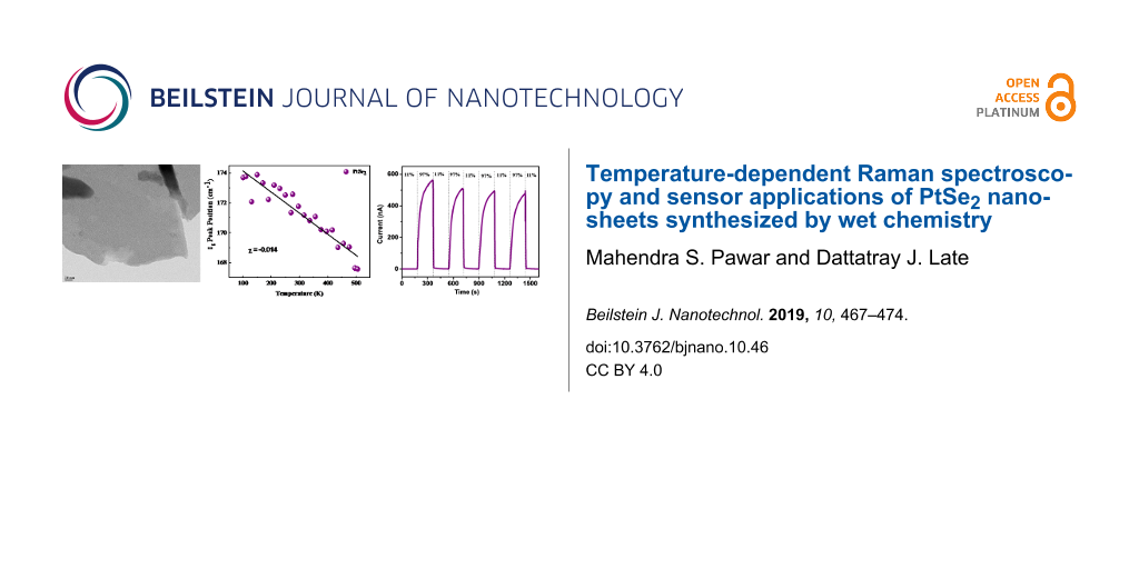
The temperature-dependent Raman spectroscopy investigations of few-layer PtSe2 nanosheets were carried out between 100–506 K. The Raman spectra of the PtSe2 nanosheets at different temperatures are provided in Supporting Information File 1, Figures S2 and S3. The Raman mode Eg and A1g as a function of temperature is shown in Figure 6a,b. It can be clearly seen that the position of the A1g and Eg modes shifts to lower wavenumbers as the temperature increases from 100 K to 506 K. The Raman modes Eg and A1g for PtSe2 behave linearly within the temperature range 100–506 K. Furthermore, it was observed that the full width half maximum (FWHM) increases with an increase in temperature. The peak positions in the Raman spectra were calculated by fitting the Lorentzian function to the A1g and Eg modes. The temperature coefficient can be calculated by Equation 1 [29]:
![[2190-4286-10-46-i1]](/bjnano/content/inline/2190-4286-10-46-i1.svg?max-width=590&scale=1.18182)
where ω0 is the peak position of the A1g and Eg mode at zero Kelvin, χ is the temperature coefficient of the A1g and Eg modes, and ω is a Raman phonon frequency. The slope of the Raman modes vs temperature plot directly gives the value of the temperature coefficient and is given in Table 1. Further, it was clearly seen that the Raman peak position and peak broadening was affected by temperature. This change in Raman modes is mainly due to the contribution from the thermal anharmonicity. The Raman phonon frequency as a function of volume and temperature is given by Equation 2 [30]:
![[2190-4286-10-46-i2]](/bjnano/content/inline/2190-4286-10-46-i2.svg?max-width=590&scale=1.18182)
where γ is the volume thermal coefficient and K represents the isothermal volume compressibility. The first term on the right hand side, −γ/K (∂lnω/∂P)T, represents the volume contribution at a constant temperature. The second term, (∂lnω/∂T)V, represents the temperature contribution at constant volume. In single-layer TMDCs due to the direct band gap, the double resonance phenomenon is useful to explain the change in FWHM, intensity and the peak shift as a function of temperature. The double resonance phenomenon can be attributed to several process including absorption of an incident photon, creation of a hole pair, double scattering of a created hole pair by phonon, and recombination of an electron–hole pair with emission of phonon. The temperature coefficient for the Eg and A1g modes was found to be −0.014 and −0.008, respectively. The nature of the temperature dependence of the Raman spectra of PtSe2 nanosheets is found to be similar in nature to that of graphene and other 2D materials such as MoS2, WS2, MoSe2, WSe2, BP, TiS3, multilayer graphene, and MoTe2 [29,31-34]. A comparison of the temperature coefficient values corresponding to various 2D materials are shown in Table 2. The value of Δω for both Eg and A1g modes was found to be 6.11 cm−1 and 3.14 cm−1, respectively.
![[2190-4286-10-46-6]](/bjnano/content/figures/2190-4286-10-46-6.png?scale=2.0&max-width=1024&background=FFFFFF)
Figure 6: Temperature-dependent Raman spectra analysis for PtSe2 nanosheets for the (a) Eg mode and the (b) A1g mode as a function of temperature.
Figure 6: Temperature-dependent Raman spectra analysis for PtSe2 nanosheets for the (a) Eg mode and the (b) A...
Table 2: Temperature coefficient values for various 2D materials.
| TMDCs | Raman modes | Temperature coefficient (χ) | ∆ω (cm−1) | Ref. |
|---|---|---|---|---|
| MoSe2 | A1g | −0.0096 | 4.75 | [29] |
| WSe2 | A1g | −0.0071 | 3.81 | [29] |
| MoS2 | Eg | −0.0136 | 8 | [29] |
| A1g | −0.0113 | 6.11 | ||
| WS2 | Eg | −0.0098 | 4.51 | [29] |
| A1g | −0.014 | 6.43 | ||
| black phosphorous | A1g | −0.008 | 4.39 | [31] |
| B2g | −0.013 | 8.14 | ||
| A2g | −0.014 | 8.63 | ||
| TiS3 | A1g | −0.022, −0.025, −0.024, −0.017 | – | [32] |
| single-layer graphene | G | −0.0162 | – | [33] |
| bilayer graphene | G | −0.0154 | – | |
| MoTe2 (bilayer) | E’2g | −0.0116 | – | [34] |
| B’2g | −0.0181 | – | ||
| PtSe2 | Eg | −0.014 | 6.11 | this work |
| A1g | −0.008 | 3.14 | ||
Humidity sensor and photodetector based on few-layer PtSe2 nanosheets
Figure 7a shows the typical resistance of the sensor device vs relative humidity plot. The resistance is significantly decreased from 3.75 GΩ to 0.83 MΩ. The humidity sensing mechanism for the PtSe2 sensor can be explained as follows. When the PtSe2 nanosheet sensor device was exposed to water molecules/vapors, a charge transfer between the water molecules and the PtSe2 nanosheets occurs. This results in the decrease in resistance of the PtSe2 nanosheet sensor device with an increase in the relative humidity. The interactions among the water molecules (electron donor) and the PtSe2 nanosheets results in an enhancement in the conductivity of the sensor device, similar to that observed for other 2D materials such as SnSe2 [35], MoS2 [36], BP [26], and MoSe2 [37]. Figure 7b shows a typical current–time (I–t) plot where cycles of 11.3% and 97.3% RH levels were used to calculate the response and recovery time. The response and recovery time for the PtSe2-based humidity sensor device was found to be 118 s and 5 s, respectively. The advantage of the PtSe2-based humidity sensor device is its rapid recovery and its functionality at room temperature. Figure 7c shows a typical I–V plot in dark conditions and under green light illumination. Figure 7d shows the I–t plot for the photodetector based on PtSe2 nanosheets with a response time of ≈110 s and a recovery time of ≈129 s.
![[2190-4286-10-46-7]](/bjnano/content/figures/2190-4286-10-46-7.png?scale=2.0&max-width=1024&background=FFFFFF)
Figure 7: PtSe2 nanosheet based humidity sensor: (a) Typical resistance versus relative humidity plot and (b) current–time (I–t) plot taken after switching 11% RH and 97% RH. The photodetector application of PtSe2 nanosheets: (c) I–V in dark conditions and with green LED light and (d) typical I–t cycle when the LED is on and off, showing a favourable response.
Figure 7: PtSe2 nanosheet based humidity sensor: (a) Typical resistance versus relative humidity plot and (b)...
Conclusion
In conclusion, we report on a wet chemistry method to grow PtSe2 nanosheets. The SEM and TEM analysis confirm the formation of PtSe2 nanosheets. Further, the XRD, Raman and SAED pattern results were used to analyze the crystal structure and to confirm the formation of the PtSe2 phase. Temperature-dependent Raman spectroscopy investigations were carried out on PtSe2 nanosheet films grown on Si substrates between 100–506 K. The temperature coefficient for the Eg and A1g modes was found to be −0.014 and −0.008, respectively. A room temperature humidity sensor based on the PtSe2 nanosheets demonstrated an excellent recovery time of ≈5 s, indicating the great potential of PtSe2-based sensors for future nanoelectronics and sensor devices.
Supporting Information
| Supporting Information File 1: Additional figures. | ||
| Format: PDF | Size: 404.3 KB | Download |
References
-
Geim, A. K.; Novoselov, K. S. Nat. Mater. 2007, 6, 183–191. doi:10.1038/nmat1849
Return to citation in text: [1] -
Grigorenko, A. N.; Polini, M.; Novoselov, K. S. Nat. Photonics 2012, 6, 749–758. doi:10.1038/nphoton.2012.262
Return to citation in text: [1] -
Stankovich, S.; Dikin, D. A.; Dommett, G. H. B.; Kohlhaas, K. M.; Zimney, E. J.; Stach, E. A.; Piner, R. D.; Nguyen, S. T.; Ruoff, R. S. Nature 2006, 442, 282–286. doi:10.1038/nature04969
Return to citation in text: [1] -
Zhao, X.; Zhang, Q.; Chen, D.; Lu, P. Macromolecules 2010, 43, 2357–2363. doi:10.1021/ma902862u
Return to citation in text: [1] -
Pawbake, A. S.; Mishra, K. K.; Machuno, L. G. B.; Gelamo, R. V.; Ravindran, T. R.; Rout, C. S.; Late, D. J. Diamond Relat. Mater. 2018, 84, 146–156. doi:10.1016/j.diamond.2018.03.021
Return to citation in text: [1] -
Liu, W.; Luo, X.; Bao, Y.; Liu, Y. P.; Ning, G.-H.; Abdelwahab, I.; Li, L.; Nai, C. T.; Hu, Z. G.; Zhao, D.; Liu, B.; Quek, S. Y.; Loh, K. P. Nat. Chem. 2017, 9, 563–570. doi:10.1038/nchem.2696
Return to citation in text: [1] -
Wang, Q. H.; Kalantar-Zadeh, K.; Kis, A.; Coleman, J. N.; Strano, M. S. Nat. Nanotechnol. 2012, 7, 699–712. doi:10.1038/nnano.2012.193
Return to citation in text: [1] -
Peng, B.; Ang, P. K.; Loh, K. P. Nano Today 2015, 10, 128–137. doi:10.1016/j.nantod.2015.01.007
Return to citation in text: [1] -
Li, H.; Shi, Y.; Chiu, M.-H.; Li, L.-J. Nano Energy 2015, 18, 293–305. doi:10.1016/j.nanoen.2015.10.023
Return to citation in text: [1] -
Jariwala, D.; Sangwan, V. K.; Lauhon, L. J.; Marks, T. J.; Hersam, M. C. ACS Nano 2014, 8, 1102–1120. doi:10.1021/nn500064s
Return to citation in text: [1] -
Shi, J.; Ma, D.; Han, G.-F.; Zhang, Y.; Ji, Q.; Gao, T.; Sun, J.; Song, X.; Li, C.; Zhang, Y.; Lang, X.-Y.; Zhang, Y.; Liu, Z. ACS Nano 2014, 8, 10196–10204. doi:10.1021/nn503211t
Return to citation in text: [1] -
Voiry, D.; Salehi, M.; Silva, R.; Fujita, T.; Chen, M.; Asefa, T.; Shenoy, V. B.; Eda, G.; Chhowalla, M. Nano Lett. 2013, 13, 6222–6227. doi:10.1021/nl403661s
Return to citation in text: [1] -
Splendiani, A.; Sun, L.; Zhang, Y.; Li, T.; Kim, J.; Chim, C.-Y.; Galli, G.; Wang, F. Nano Lett. 2010, 10, 1271–1275. doi:10.1021/nl903868w
Return to citation in text: [1] -
Tongay, S.; Zhou, J.; Ataca, C.; Lo, K.; Matthews, T. S.; Li, J.; Grossman, J. C.; Wu, J. Nano Lett. 2012, 12, 5576–5580. doi:10.1021/nl302584w
Return to citation in text: [1] -
Zhang, Y.; Chang, T.-R.; Zhou, B.; Cui, Y.-T.; Yan, H.; Liu, Z.; Schmitt, F.; Lee, J.; Moore, R.; Chen, Y.; Lin, H.; Jeng, H.-T.; Mo, S.-K.; Hussain, Z.; Bansil, A.; Shen, Z.-X. Nat. Nanotechnol. 2014, 9, 111–115. doi:10.1038/nnano.2013.277
Return to citation in text: [1] -
Mak, K. F.; Lee, C.; Hone, J.; Shan, J.; Heinz, T. F. Phys. Rev. Lett. 2010, 105, 136805–136808. doi:10.1103/physrevlett.105.136805
Return to citation in text: [1] -
Sundaram, R. S.; Engel, M.; Lombardo, A.; Krupke, R.; Ferrari, A. C.; Avouris, P.; Steiner, M. Nano Lett. 2013, 13, 1416–1421. doi:10.1021/nl400516a
Return to citation in text: [1] -
Guo, G. Y.; Liang, W. Y. J. Phys. C: Solid State Phys. 1986, 19, 995–1008. doi:10.1088/0022-3719/19/7/011
Return to citation in text: [1] -
Wang, Y.; Li, L.; Yao, W.; Song, S.; Sun, J. T.; Pan, J.; Ren, X.; Li, C.; Okunishi, E.; Wang, Y.-Q.; Wang, E.; Shao, Y.; Zhang, Y. Y.; Yang, H.-t.; Schwier, E. F.; Iwasawa, H.; Shimada, K.; Taniguchi, M.; Cheng, Z.; Zhou, S.; Du, S.; Pennycook, S. J.; Pantelides, S. T.; Gao, H.-J. Nano Lett. 2015, 15, 4013–4018. doi:10.1021/acs.nanolett.5b00964
Return to citation in text: [1] [2] [3] -
Zhao, Y.; Qiao, J.; Yu, Z.; Yu, P.; Xu, K.; Lau, S. P.; Zhou, W.; Liu, Z.; Wang, X.; Ji, W.; Chai, Y. Adv. Mater. (Weinheim, Ger.) 2017, 29, 1604230. doi:10.1002/adma.201604230
Return to citation in text: [1] -
Sattar, S.; Schwingenschlögl, U. ACS Appl. Mater. Interfaces 2017, 9, 15809–15813. doi:10.1021/acsami.7b00012
Return to citation in text: [1] -
O’Brien, M.; McEvoy, N.; Motta, C.; Zheng, J.-Y.; Berner, N. C.; Kotakoski, J.; Elibol, K.; Pennycook, T. J.; Meyer, J. C.; Yim, C.; Abid, M.; Hallam, T.; Donegan, J. F.; Sanvito, S.; Duesberg, G. S. 2D Mater. 2016, 3, 021004. doi:10.1088/2053-1583/3/2/021004
Return to citation in text: [1] [2] -
Grønvold, F.; Haraldsen, H.; Kjekshus, A.; Söderquist, R. Acta Chem. Scand. 1960, 14, 1879–1893. doi:10.3891/acta.chem.scand.14-1879
Return to citation in text: [1] -
Yim, C.; Lee, K.; McEvoy, N.; O’Brien, M.; Riazimehr, S.; Berner, N. C.; Cullen, C. P.; Kotakoski, J.; Meyer, J. C.; Lemme, M. C.; Duesberg, G. S. ACS Nano 2016, 10, 9550–9558. doi:10.1021/acsnano.6b04898
Return to citation in text: [1] [2] -
Ali Umar, A.; Md Saad, S. K.; Mat Salleh, M. ACS Omega 2017, 2, 3325–3332. doi:10.1021/acsomega.7b00580
Return to citation in text: [1] [2] -
Erande, M. B.; Pawar, M. S.; Late, D. J. ACS Appl. Mater. Interfaces 2016, 8, 11548–11556. doi:10.1021/acsami.5b10247
Return to citation in text: [1] [2] -
Yu, X.; Yu, P.; Wu, D.; Singh, B.; Zeng, Q.; Lin, H.; Zhou, W.; Lin, J.; Suenaga, K.; Liu, Z.; Wang, Q. J. Nat. Commun. 2018, 9, 1545. doi:10.1038/s41467-018-03935-0
Return to citation in text: [1] -
Zhang, K.; Yan, M.; Zhang, H.; Huang, H.; Arita, M.; Sun, Z.; Duan, W.; Wu, Y.; Zhou, S. Phys. Rev. B 2017, 96, 125102. doi:10.1103/physrevb.96.125102
Return to citation in text: [1] -
Pawbake, A. S.; Pawar, M. S.; Jadkar, S. R.; Late, D. J. Nanoscale 2016, 8, 3008–3018. doi:10.1039/c5nr07401k
Return to citation in text: [1] [2] [3] [4] [5] [6] -
Late, D. J.; Maitra, U.; Panchakarla, L. S.; Waghmare, U. V.; Rao, C. N. R. J. Phys.: Condens. Matter 2011, 23, 055303. doi:10.1088/0953-8984/23/5/055303
Return to citation in text: [1] -
Late, D. J. ACS Appl. Mater. Interfaces 2015, 7, 5857–5862. doi:10.1021/am509056b
Return to citation in text: [1] [2] -
Pawbake, A. S.; Island, J. O.; Flores, E.; Ares, J. R.; Sanchez, C.; Ferrer, I. J.; Jadkar, S. R.; van der Zant, H. S. J.; Castellanos-Gomez, A.; Late, D. J. ACS Appl. Mater. Interfaces 2015, 7, 24185–24190. doi:10.1021/acsami.5b07492
Return to citation in text: [1] [2] -
Calizo, I.; Balandin, A. A.; Bao, W.; Miao, F.; Lau, C. N. Nano Lett. 2007, 7, 2645–2649. doi:10.1021/nl071033g
Return to citation in text: [1] [2] -
Late, D. J. Appl. Mater. Today 2016, 5, 98–102. doi:10.1016/j.apmt.2016.09.013
Return to citation in text: [1] [2] -
Pawar, M.; Kadam, S.; Late, D. J. ChemistrySelect 2017, 2, 4068–4075. doi:10.1002/slct.201700261
Return to citation in text: [1] -
Late, D. J.; Huang, Y.-K.; Liu, B.; Acharya, J.; Shirodkar, S. N.; Luo, J.; Yan, A.; Charles, D.; Waghmare, U. V.; Dravid, V. P.; Rao, C. N. R. ACS Nano 2013, 7, 4879–4891. doi:10.1021/nn400026u
Return to citation in text: [1] -
Late, D. J.; Doneux, T.; Bougouma, M. Appl. Phys. Lett. 2014, 105, 233103. doi:10.1063/1.4903358
Return to citation in text: [1]
| 35. | Pawar, M.; Kadam, S.; Late, D. J. ChemistrySelect 2017, 2, 4068–4075. doi:10.1002/slct.201700261 |
| 36. | Late, D. J.; Huang, Y.-K.; Liu, B.; Acharya, J.; Shirodkar, S. N.; Luo, J.; Yan, A.; Charles, D.; Waghmare, U. V.; Dravid, V. P.; Rao, C. N. R. ACS Nano 2013, 7, 4879–4891. doi:10.1021/nn400026u |
| 26. | Erande, M. B.; Pawar, M. S.; Late, D. J. ACS Appl. Mater. Interfaces 2016, 8, 11548–11556. doi:10.1021/acsami.5b10247 |
| 1. | Geim, A. K.; Novoselov, K. S. Nat. Mater. 2007, 6, 183–191. doi:10.1038/nmat1849 |
| 13. | Splendiani, A.; Sun, L.; Zhang, Y.; Li, T.; Kim, J.; Chim, C.-Y.; Galli, G.; Wang, F. Nano Lett. 2010, 10, 1271–1275. doi:10.1021/nl903868w |
| 14. | Tongay, S.; Zhou, J.; Ataca, C.; Lo, K.; Matthews, T. S.; Li, J.; Grossman, J. C.; Wu, J. Nano Lett. 2012, 12, 5576–5580. doi:10.1021/nl302584w |
| 15. | Zhang, Y.; Chang, T.-R.; Zhou, B.; Cui, Y.-T.; Yan, H.; Liu, Z.; Schmitt, F.; Lee, J.; Moore, R.; Chen, Y.; Lin, H.; Jeng, H.-T.; Mo, S.-K.; Hussain, Z.; Bansil, A.; Shen, Z.-X. Nat. Nanotechnol. 2014, 9, 111–115. doi:10.1038/nnano.2013.277 |
| 16. | Mak, K. F.; Lee, C.; Hone, J.; Shan, J.; Heinz, T. F. Phys. Rev. Lett. 2010, 105, 136805–136808. doi:10.1103/physrevlett.105.136805 |
| 17. | Sundaram, R. S.; Engel, M.; Lombardo, A.; Krupke, R.; Ferrari, A. C.; Avouris, P.; Steiner, M. Nano Lett. 2013, 13, 1416–1421. doi:10.1021/nl400516a |
| 22. | O’Brien, M.; McEvoy, N.; Motta, C.; Zheng, J.-Y.; Berner, N. C.; Kotakoski, J.; Elibol, K.; Pennycook, T. J.; Meyer, J. C.; Yim, C.; Abid, M.; Hallam, T.; Donegan, J. F.; Sanvito, S.; Duesberg, G. S. 2D Mater. 2016, 3, 021004. doi:10.1088/2053-1583/3/2/021004 |
| 28. | Zhang, K.; Yan, M.; Zhang, H.; Huang, H.; Arita, M.; Sun, Z.; Duan, W.; Wu, Y.; Zhou, S. Phys. Rev. B 2017, 96, 125102. doi:10.1103/physrevb.96.125102 |
| 7. | Wang, Q. H.; Kalantar-Zadeh, K.; Kis, A.; Coleman, J. N.; Strano, M. S. Nat. Nanotechnol. 2012, 7, 699–712. doi:10.1038/nnano.2012.193 |
| 8. | Peng, B.; Ang, P. K.; Loh, K. P. Nano Today 2015, 10, 128–137. doi:10.1016/j.nantod.2015.01.007 |
| 9. | Li, H.; Shi, Y.; Chiu, M.-H.; Li, L.-J. Nano Energy 2015, 18, 293–305. doi:10.1016/j.nanoen.2015.10.023 |
| 10. | Jariwala, D.; Sangwan, V. K.; Lauhon, L. J.; Marks, T. J.; Hersam, M. C. ACS Nano 2014, 8, 1102–1120. doi:10.1021/nn500064s |
| 11. | Shi, J.; Ma, D.; Han, G.-F.; Zhang, Y.; Ji, Q.; Gao, T.; Sun, J.; Song, X.; Li, C.; Zhang, Y.; Lang, X.-Y.; Zhang, Y.; Liu, Z. ACS Nano 2014, 8, 10196–10204. doi:10.1021/nn503211t |
| 12. | Voiry, D.; Salehi, M.; Silva, R.; Fujita, T.; Chen, M.; Asefa, T.; Shenoy, V. B.; Eda, G.; Chhowalla, M. Nano Lett. 2013, 13, 6222–6227. doi:10.1021/nl403661s |
| 24. | Yim, C.; Lee, K.; McEvoy, N.; O’Brien, M.; Riazimehr, S.; Berner, N. C.; Cullen, C. P.; Kotakoski, J.; Meyer, J. C.; Lemme, M. C.; Duesberg, G. S. ACS Nano 2016, 10, 9550–9558. doi:10.1021/acsnano.6b04898 |
| 6. | Liu, W.; Luo, X.; Bao, Y.; Liu, Y. P.; Ning, G.-H.; Abdelwahab, I.; Li, L.; Nai, C. T.; Hu, Z. G.; Zhao, D.; Liu, B.; Quek, S. Y.; Loh, K. P. Nat. Chem. 2017, 9, 563–570. doi:10.1038/nchem.2696 |
| 26. | Erande, M. B.; Pawar, M. S.; Late, D. J. ACS Appl. Mater. Interfaces 2016, 8, 11548–11556. doi:10.1021/acsami.5b10247 |
| 2. | Grigorenko, A. N.; Polini, M.; Novoselov, K. S. Nat. Photonics 2012, 6, 749–758. doi:10.1038/nphoton.2012.262 |
| 3. | Stankovich, S.; Dikin, D. A.; Dommett, G. H. B.; Kohlhaas, K. M.; Zimney, E. J.; Stach, E. A.; Piner, R. D.; Nguyen, S. T.; Ruoff, R. S. Nature 2006, 442, 282–286. doi:10.1038/nature04969 |
| 4. | Zhao, X.; Zhang, Q.; Chen, D.; Lu, P. Macromolecules 2010, 43, 2357–2363. doi:10.1021/ma902862u |
| 5. | Pawbake, A. S.; Mishra, K. K.; Machuno, L. G. B.; Gelamo, R. V.; Ravindran, T. R.; Rout, C. S.; Late, D. J. Diamond Relat. Mater. 2018, 84, 146–156. doi:10.1016/j.diamond.2018.03.021 |
| 27. | Yu, X.; Yu, P.; Wu, D.; Singh, B.; Zeng, Q.; Lin, H.; Zhou, W.; Lin, J.; Suenaga, K.; Liu, Z.; Wang, Q. J. Nat. Commun. 2018, 9, 1545. doi:10.1038/s41467-018-03935-0 |
| 23. | Grønvold, F.; Haraldsen, H.; Kjekshus, A.; Söderquist, R. Acta Chem. Scand. 1960, 14, 1879–1893. doi:10.3891/acta.chem.scand.14-1879 |
| 25. | Ali Umar, A.; Md Saad, S. K.; Mat Salleh, M. ACS Omega 2017, 2, 3325–3332. doi:10.1021/acsomega.7b00580 |
| 20. | Zhao, Y.; Qiao, J.; Yu, Z.; Yu, P.; Xu, K.; Lau, S. P.; Zhou, W.; Liu, Z.; Wang, X.; Ji, W.; Chai, Y. Adv. Mater. (Weinheim, Ger.) 2017, 29, 1604230. doi:10.1002/adma.201604230 |
| 21. | Sattar, S.; Schwingenschlögl, U. ACS Appl. Mater. Interfaces 2017, 9, 15809–15813. doi:10.1021/acsami.7b00012 |
| 22. | O’Brien, M.; McEvoy, N.; Motta, C.; Zheng, J.-Y.; Berner, N. C.; Kotakoski, J.; Elibol, K.; Pennycook, T. J.; Meyer, J. C.; Yim, C.; Abid, M.; Hallam, T.; Donegan, J. F.; Sanvito, S.; Duesberg, G. S. 2D Mater. 2016, 3, 021004. doi:10.1088/2053-1583/3/2/021004 |
| 25. | Ali Umar, A.; Md Saad, S. K.; Mat Salleh, M. ACS Omega 2017, 2, 3325–3332. doi:10.1021/acsomega.7b00580 |
| 19. | Wang, Y.; Li, L.; Yao, W.; Song, S.; Sun, J. T.; Pan, J.; Ren, X.; Li, C.; Okunishi, E.; Wang, Y.-Q.; Wang, E.; Shao, Y.; Zhang, Y. Y.; Yang, H.-t.; Schwier, E. F.; Iwasawa, H.; Shimada, K.; Taniguchi, M.; Cheng, Z.; Zhou, S.; Du, S.; Pennycook, S. J.; Pantelides, S. T.; Gao, H.-J. Nano Lett. 2015, 15, 4013–4018. doi:10.1021/acs.nanolett.5b00964 |
| 37. | Late, D. J.; Doneux, T.; Bougouma, M. Appl. Phys. Lett. 2014, 105, 233103. doi:10.1063/1.4903358 |
| 18. | Guo, G. Y.; Liang, W. Y. J. Phys. C: Solid State Phys. 1986, 19, 995–1008. doi:10.1088/0022-3719/19/7/011 |
| 19. | Wang, Y.; Li, L.; Yao, W.; Song, S.; Sun, J. T.; Pan, J.; Ren, X.; Li, C.; Okunishi, E.; Wang, Y.-Q.; Wang, E.; Shao, Y.; Zhang, Y. Y.; Yang, H.-t.; Schwier, E. F.; Iwasawa, H.; Shimada, K.; Taniguchi, M.; Cheng, Z.; Zhou, S.; Du, S.; Pennycook, S. J.; Pantelides, S. T.; Gao, H.-J. Nano Lett. 2015, 15, 4013–4018. doi:10.1021/acs.nanolett.5b00964 |
| 19. | Wang, Y.; Li, L.; Yao, W.; Song, S.; Sun, J. T.; Pan, J.; Ren, X.; Li, C.; Okunishi, E.; Wang, Y.-Q.; Wang, E.; Shao, Y.; Zhang, Y. Y.; Yang, H.-t.; Schwier, E. F.; Iwasawa, H.; Shimada, K.; Taniguchi, M.; Cheng, Z.; Zhou, S.; Du, S.; Pennycook, S. J.; Pantelides, S. T.; Gao, H.-J. Nano Lett. 2015, 15, 4013–4018. doi:10.1021/acs.nanolett.5b00964 |
| 24. | Yim, C.; Lee, K.; McEvoy, N.; O’Brien, M.; Riazimehr, S.; Berner, N. C.; Cullen, C. P.; Kotakoski, J.; Meyer, J. C.; Lemme, M. C.; Duesberg, G. S. ACS Nano 2016, 10, 9550–9558. doi:10.1021/acsnano.6b04898 |
| 29. | Pawbake, A. S.; Pawar, M. S.; Jadkar, S. R.; Late, D. J. Nanoscale 2016, 8, 3008–3018. doi:10.1039/c5nr07401k |
| 31. | Late, D. J. ACS Appl. Mater. Interfaces 2015, 7, 5857–5862. doi:10.1021/am509056b |
| 32. | Pawbake, A. S.; Island, J. O.; Flores, E.; Ares, J. R.; Sanchez, C.; Ferrer, I. J.; Jadkar, S. R.; van der Zant, H. S. J.; Castellanos-Gomez, A.; Late, D. J. ACS Appl. Mater. Interfaces 2015, 7, 24185–24190. doi:10.1021/acsami.5b07492 |
| 33. | Calizo, I.; Balandin, A. A.; Bao, W.; Miao, F.; Lau, C. N. Nano Lett. 2007, 7, 2645–2649. doi:10.1021/nl071033g |
| 34. | Late, D. J. Appl. Mater. Today 2016, 5, 98–102. doi:10.1016/j.apmt.2016.09.013 |
| 29. | Pawbake, A. S.; Pawar, M. S.; Jadkar, S. R.; Late, D. J. Nanoscale 2016, 8, 3008–3018. doi:10.1039/c5nr07401k |
| 30. | Late, D. J.; Maitra, U.; Panchakarla, L. S.; Waghmare, U. V.; Rao, C. N. R. J. Phys.: Condens. Matter 2011, 23, 055303. doi:10.1088/0953-8984/23/5/055303 |
| 33. | Calizo, I.; Balandin, A. A.; Bao, W.; Miao, F.; Lau, C. N. Nano Lett. 2007, 7, 2645–2649. doi:10.1021/nl071033g |
| 34. | Late, D. J. Appl. Mater. Today 2016, 5, 98–102. doi:10.1016/j.apmt.2016.09.013 |
| 31. | Late, D. J. ACS Appl. Mater. Interfaces 2015, 7, 5857–5862. doi:10.1021/am509056b |
| 32. | Pawbake, A. S.; Island, J. O.; Flores, E.; Ares, J. R.; Sanchez, C.; Ferrer, I. J.; Jadkar, S. R.; van der Zant, H. S. J.; Castellanos-Gomez, A.; Late, D. J. ACS Appl. Mater. Interfaces 2015, 7, 24185–24190. doi:10.1021/acsami.5b07492 |
| 29. | Pawbake, A. S.; Pawar, M. S.; Jadkar, S. R.; Late, D. J. Nanoscale 2016, 8, 3008–3018. doi:10.1039/c5nr07401k |
| 29. | Pawbake, A. S.; Pawar, M. S.; Jadkar, S. R.; Late, D. J. Nanoscale 2016, 8, 3008–3018. doi:10.1039/c5nr07401k |
| 29. | Pawbake, A. S.; Pawar, M. S.; Jadkar, S. R.; Late, D. J. Nanoscale 2016, 8, 3008–3018. doi:10.1039/c5nr07401k |
| 29. | Pawbake, A. S.; Pawar, M. S.; Jadkar, S. R.; Late, D. J. Nanoscale 2016, 8, 3008–3018. doi:10.1039/c5nr07401k |
© 2019 Pawar and Late; licensee Beilstein-Institut.
This is an Open Access article under the terms of the Creative Commons Attribution License (http://creativecommons.org/licenses/by/4.0). Please note that the reuse, redistribution and reproduction in particular requires that the authors and source are credited.
The license is subject to the Beilstein Journal of Nanotechnology terms and conditions: (https://www.beilstein-journals.org/bjnano)