Abstract
We investigate superconductor–insulator quantum phase transitions in ultrathin capacitively coupled superconducting nanowires with proliferating quantum phase slips. We derive a set of coupled Berezinskii–Kosterlitz–Thouless-like renormalization group equations demonstrating that interaction between quantum phase slips in one of the wires gets modified due to the effect of plasma modes propagating in another wire. As a result, the superconductor–insulator phase transition in each of the wires is controlled not only by its own parameters but also by those of the neighboring wire as well as by mutual capacitance. We argue that superconducting nanowires with properly chosen parameters may turn insulating once they are brought sufficiently close to each other.
Introduction
Quantum fluctuations dominate the physics of superconducting nanowires at sufficiently low temperatures making their behavior markedly different from that of bulk superconductors [1-4]. Many interesting properties of such nanowires are attributed to the effect of quantum phase slips (QPSs) which correspond to fluctuation-induced local temporal suppression of the superconducting order parameter inside the wire accompanied by the phase slippage process and quantum fluctuations of the voltage in the form of pulses. By applying a bias current the symmetry between positive and negative voltage pulses is broken and, as a result, a superconducting nanowire acquires a non-vanishing electrical resistance down to the lowest temperatures [5,6]. This effect was directly observed in a number of experiments [7-10].
Likewise, quantum phase slips in superconducting nanowires yield shot noise of the voltage [11] which originates from the process of quantum tunneling of magnetic flux quanta across the wire. One can also proceed beyond the voltage–voltage correlator and evaluate all cumulants of the voltage operator, thus deriving full counting statistics of quantum phase slips [12]. This theory enables one to obtain a complete description of superconducting fluctuations in such nanowires. Interesting QPS-related effects also occur in superconducting nanorings which can be employed, for example, for possible realization of superconducting qubits [13]. Such effects were investigated theoretically [14] and observed experimentally [15,16].
Each quantum phase slip generates sound-like plasma modes [17] which propagate along the wire and interact with other QPSs. The exchange of such Mooij–Schön plasmons produces a logarithmic interaction in space–time between different QPSs where the magnitude is controlled by the wire diameter (cross section) [5]. For sufficiently thick wires this interaction is strong and the QPSs are bound in close pairs. Accordingly, the (linear) resistance of such wires tends to zero at T → 0, thus demonstrating a superconducting-like behavior in this limit. On the other hand, inter-QPS interaction in ultrathin wires is weak, quantum phase slips are unbound and the superconducting phase fluctuates strongly along the wire. In this case the wire looses long-scale superconducting properties, its total resistance remains non-zero and even tends to increase with decreasing temperature thus indicating an insulating behavior at T → 0. At zero temperature the transition between these two types of behavior comes as a quantum phase transition (QPT) driven by the wire diameter [5]. Below we will also refer to this QPT as a superconductor–insulator transition (SIT).
In this work we will show that this SIT can be substantially modified in a system of capacitively coupled superconducting nanowires even without any direct electrical contact between them. In our previous work [18] we already elucidated some non-local QPS-related effects in such nanowires which yield non-equilibrium voltage fluctuations in the system which exhibit a non-trivial dependence on frequency and bias current. Here we will demonstrate that quantum fluctuations in one of the two wires effectively ”add up” to those of another one, thereby shifting the QPT in each of the wires in a way to increase the parameter range for the insulating phase. Qualitatively the same effect is expected to occur in a single superconducting nanowire that has the form of a meander frequently used in experiments.
Results and Discussion
The model
We first consider the system of two long superconducting nanowires parallel to each other, as schematically shown in Figure 1a.
![[2190-4286-11-124-1]](/bjnano/content/figures/2190-4286-11-124-1.png?scale=2.0&max-width=1024&background=FFFFFF)
Figure 1: The systems under consideration: a) Two capacitively coupled superconducting nanowires and b) a superconducting nanowire in the form of a meander.
Figure 1: The systems under consideration: a) Two capacitively coupled superconducting nanowires and b) a sup...
The wires are described by geometric capacitances C1 and C2 (per unit wire length) and kinetic inductances ![[Graphic 1]](/bjnano/content/inline/2190-4286-11-124-i23.svg?max-width=637&scale=1.18182) and
and ![[Graphic 2]](/bjnano/content/inline/2190-4286-11-124-i24.svg?max-width=637&scale=1.18182) (times length) effectively representing the two transmission lines. Capacitive coupling between these two nanowires is accounted for by the mutual capacitance Cm. The corresponding contribution to the system Hamiltonian that keeps track of both electric and magnetic energies in these coupled transmission lines reads
(times length) effectively representing the two transmission lines. Capacitive coupling between these two nanowires is accounted for by the mutual capacitance Cm. The corresponding contribution to the system Hamiltonian that keeps track of both electric and magnetic energies in these coupled transmission lines reads
![[2190-4286-11-124-i1]](/bjnano/content/inline/2190-4286-11-124-i1.svg?max-width=590&scale=1.18182)
where x is the coordinate along the wires, ![[Graphic 3]](/bjnano/content/inline/2190-4286-11-124-i25.svg?max-width=637&scale=1.18182) and Cij denote the matrix elements of the inductance and capacitance matrices
and Cij denote the matrix elements of the inductance and capacitance matrices
![[2190-4286-11-124-i2]](/bjnano/content/inline/2190-4286-11-124-i2.svg?max-width=590&scale=1.18182)
and Φ0 = π/e is the superconducting flux quantum. Note that for the sake of simplicity here and below we set Planck constant ℏ, speed of light, c, and Boltzmann constant, kB, equal to unity.
The Hamiltonian (Equation 1) is expressed in terms of the dual operators ![[Graphic 4]](/bjnano/content/inline/2190-4286-11-124-i26.svg?max-width=637&scale=1.18182) and
and ![[Graphic 5]](/bjnano/content/inline/2190-4286-11-124-i27.svg?max-width=637&scale=1.18182) [14] which obey the canonical commutation relation
[14] which obey the canonical commutation relation
![[2190-4286-11-124-i3]](/bjnano/content/inline/2190-4286-11-124-i3.svg?max-width=590&scale=1.18182)
and are related to the charge density and the local phase operators, ![[Graphic 6]](/bjnano/content/inline/2190-4286-11-124-i28.svg?max-width=637&scale=1.18182) and
and ![[Graphic 7]](/bjnano/content/inline/2190-4286-11-124-i29.svg?max-width=637&scale=1.18182) respectively, by means of the following equations
respectively, by means of the following equations
![[2190-4286-11-124-i4]](/bjnano/content/inline/2190-4286-11-124-i4.svg?max-width=590&scale=1.18182)
Physically, ![[Graphic 8]](/bjnano/content/inline/2190-4286-11-124-i30.svg?max-width=637&scale=1.18182) represents the magnetic flux operator, while the operator
represents the magnetic flux operator, while the operator ![[Graphic 9]](/bjnano/content/inline/2190-4286-11-124-i31.svg?max-width=637&scale=1.18182) is proportional to that of the total charge
is proportional to that of the total charge ![[Graphic 10]](/bjnano/content/inline/2190-4286-11-124-i32.svg?max-width=637&scale=1.18182) that has passed through the point x of the ith wire up to the time moment t, i.e.,
that has passed through the point x of the ith wire up to the time moment t, i.e., ![[Graphic 11]](/bjnano/content/inline/2190-4286-11-124-i33.svg?max-width=637&scale=1.18182)
Provided that the wires are thick enough, the low energy Hamiltonian in Equation 1 is sufficient. However, for thinner wires, one should also account for the effect of quantum phase slips. The corresponding contribution to the total Hamiltonian for our system can be expressed in the form [14]
![[2190-4286-11-124-i5]](/bjnano/content/inline/2190-4286-11-124-i5.svg?max-width=590&scale=1.18182)
where
![[2190-4286-11-124-i6]](/bjnano/content/inline/2190-4286-11-124-i6.svg?max-width=590&scale=1.18182)
denotes the QPS amplitudes per unit wire length [6], gjξ = Rq/Rjξ is the dimensionless conductance of the jth wire segment of length equal to the superconducting coherence length ξ (here and below Rq = 2π/e2 ≃ 25.8 kΩ is the quantum resistance unit and Rjξ is the normal state resistance of the corresponding wire segment), Δ is the superconducting order parameter and a ≈ 1 is a numerical prefactor. We also note that the Hamiltonian (Equation 5) describes tunneling of the magnetic flux quantum, Φ0, across the wire and can be viewed as a linear combination of creation ![[Graphic 12]](/bjnano/content/inline/2190-4286-11-124-i34.svg?max-width=637&scale=1.18182) and annihilation
and annihilation ![[Graphic 13]](/bjnano/content/inline/2190-4286-11-124-i35.svg?max-width=637&scale=1.18182) operators for the flux quantum Φ0.
operators for the flux quantum Φ0.
It is obvious from Equation 4 that QPS events cause redistribution of charges inside the wire and generate pairs of voltage pulses moving simultaneously in the opposite direction (cf., Figure 1a)
![[2190-4286-11-124-i7]](/bjnano/content/inline/2190-4286-11-124-i7.svg?max-width=590&scale=1.18182)
Clearly, in the presence of capacitive coupling quantum phase slips in one of the wires also generate voltage pulses in another one.
To summarize the above considerations, the total Hamiltonian for our system is defined as a sum of the two terms in Equation 1 and Equation 5,
![[2190-4286-11-124-i8]](/bjnano/content/inline/2190-4286-11-124-i8.svg?max-width=590&scale=1.18182)
representing an effective sine-Gordon model that will be treated below.
Quantum phase transitions: renormalization group analysis
In order to quantitatively describe QPT in coupled superconducting wires we will employ the renormalization group (RG) analysis. This approach is well developed and was successfully applied to a variety of problems in condensed matter theory, such as, the problem of weak Coulomb blockade in tunnel [19-22] and non-tunnel [23-25] barriers between normal metals or that of a dissipative phase transition in resistively shunted Josephson junctions [19,26-28]. In the case of superconducting nanowires QPT was described [5] with the aid of RG equations equivalent to those initially developed for two-dimensional superconducting films [29] which exhibit classical Berezinskii–Kosterlitz–Thouless (BKT) phase transition driven by temperature. In contrast, quantum SIT in quasi-one-dimensional superconducting wires [5] with geometric capacitance C and kinetic inductance ![[Graphic 14]](/bjnano/content/inline/2190-4286-11-124-i36.svg?max-width=637&scale=1.18182) is controlled by the parameter [5]
is controlled by the parameter [5]
![[2190-4286-11-124-i9]](/bjnano/content/inline/2190-4286-11-124-i9.svg?max-width=590&scale=1.18182)
which is proportional to the square root of the wire cross section, s.
It follows immediately from the analysis of [5] that, provided the two superconducting wires depicted in Figure 1a are decoupled from each other (i.e., for Cm → 0), one should expect two independent QPTs to occur in these two wires respectively at λ1 = 2 and at λ2 = 2 where, according to Equation 9, we define ![[Graphic 15]](/bjnano/content/inline/2190-4286-11-124-i37.svg?max-width=637&scale=1.18182) The task at hand is to investigate the effect of capacitive coupling between the wires on these two QPTs.
The task at hand is to investigate the effect of capacitive coupling between the wires on these two QPTs.
For this purpose let us express the grand partition function of our system ![[Graphic 16]](/bjnano/content/inline/2190-4286-11-124-i38.svg?max-width=637&scale=1.18182) in terms of the path integral
in terms of the path integral
![[2190-4286-11-124-i10]](/bjnano/content/inline/2190-4286-11-124-i10.svg?max-width=590&scale=1.18182)
where
![[2190-4286-11-124-i11]](/bjnano/content/inline/2190-4286-11-124-i11.svg?max-width=590&scale=1.18182)
is the effective action corresponding to the Hamiltonian (Equation 8) and
![[2190-4286-11-124-i12]](/bjnano/content/inline/2190-4286-11-124-i12.svg?max-width=590&scale=1.18182)
denotes the effective fugacity for the gas of quantum phase slips in the ith wire. Note that, having in mind that the QPS core size in x- and τ-directions is respectively x0 ∼ ξ and τ0 ∼ Δ−1, in Equation 11 for the sake of convenience we rescaled the spatial coordinate in units of x0, i.e. x → xξ and the time coordinate in units of τ0, i.e. τ → τ/Δ.
In the spirit of Wilson’s RG approach we routinely divide the χ-variables into fast and slow components, ![[Graphic 17]](/bjnano/content/inline/2190-4286-11-124-i39.svg?max-width=637&scale=1.18182) , where
, where
![[2190-4286-11-124-i13]](/bjnano/content/inline/2190-4286-11-124-i13.svg?max-width=590&scale=1.18182)
Setting δΛ/Λ ≪ 1, expanding in the fast field components ![[Graphic 18]](/bjnano/content/inline/2190-4286-11-124-i40.svg?max-width=637&scale=1.18182) and integrating them out we proceed perturbatively in y1,2 and observe that in order to account for the leading order corrections it is necessary to evaluate the matrix Green function at coincident points which reads
and integrating them out we proceed perturbatively in y1,2 and observe that in order to account for the leading order corrections it is necessary to evaluate the matrix Green function at coincident points which reads
![[2190-4286-11-124-i14]](/bjnano/content/inline/2190-4286-11-124-i14.svg?max-width=590&scale=1.18182)
where ![[Graphic 19]](/bjnano/content/inline/2190-4286-11-124-i41.svg?max-width=637&scale=1.18182) and
and ![[Graphic 20]](/bjnano/content/inline/2190-4286-11-124-i42.svg?max-width=637&scale=1.18182) is the velocity matrix for plasmon modes propagating along the wires. The matrix
is the velocity matrix for plasmon modes propagating along the wires. The matrix ![[Graphic 21]](/bjnano/content/inline/2190-4286-11-124-i43.svg?max-width=637&scale=1.18182) has the form
has the form
![[2190-4286-11-124-i15]](/bjnano/content/inline/2190-4286-11-124-i15.svg?max-width=590&scale=1.18182)
where ![[Graphic 22]](/bjnano/content/inline/2190-4286-11-124-i44.svg?max-width=637&scale=1.18182) is the velocity of the Mooij–Schön modes in the ith wire in the absence of capacitive coupling between the wires, i.e. for Cm → 0.
is the velocity of the Mooij–Schön modes in the ith wire in the absence of capacitive coupling between the wires, i.e. for Cm → 0.
Following the standard procedure [29] and proceeding to bigger and bigger scales Λ, we eventually arrive at the following RG equations for the QPS fugacities y1 and y2:
![[2190-4286-11-124-i16]](/bjnano/content/inline/2190-4286-11-124-i16.svg?max-width=590&scale=1.18182)
where λ11 and λ22 are diagonal elements of the matrix ![[Graphic 23]](/bjnano/content/inline/2190-4286-11-124-i45.svg?max-width=637&scale=1.18182) (Equation 15). Note that here we restrict our RG analysis to the lowest order in y1,2 which is sufficient for our purposes. As long as one keeps only the linear y1,2 terms in the RG equations, all other parameters of our problem, e.g., λii, remain un-renormalized.
(Equation 15). Note that here we restrict our RG analysis to the lowest order in y1,2 which is sufficient for our purposes. As long as one keeps only the linear y1,2 terms in the RG equations, all other parameters of our problem, e.g., λii, remain un-renormalized.
As it can be observed from Equation 16, our system exhibits two BKT-like QPTs at λ11 = 2 and λ22 = 2. In the limit Cm → 0 the wires are independent from each other, λ11(22) → λ1(2) and these QPTs obviously reduce to that predicted in [5]. However, for non-zero capacitive coupling between the wires, the two QPTs occur at the values of λ1,2 exceeding 2. For the first wire the corresponding phase transition point is fixed by the condition
![[2190-4286-11-124-i17]](/bjnano/content/inline/2190-4286-11-124-i17.svg?max-width=590&scale=1.18182)
The same condition for the second wire is obtained from (Equation 17) by interchanging the indices 1 ↔ 2.
The above results allow us to conclude that in the presence of capacitive coupling SIT in both wires occurs at larger values of λ1,2 than in the absence of such coupling. In other words, quantum fluctuations in one of these wires effectively decrease the superconducting properties of the other one.
It follows from Equation 17 that the magnitude of such mutual influence depends on the ratio of the plasmon velocities in the two wires v1/v2 and on the strength of the capacitive coupling controlled by Cm. Provided the wire cross sections s1 and s2 differ strongly the plasmon velocities ![[Graphic 24]](/bjnano/content/inline/2190-4286-11-124-i46.svg?max-width=637&scale=1.18182) also differ considerably. Assume, for instance, that the first wire is much thinner than the second one. In this limit we have v1 ≪ v2 and, hence, the QPT condition (Equation 17) in the first wire remains almost unaffected for any capacitive coupling strength. If, on the contrary, the first wire is much thicker than the second one, then one has v1 ≫ v2 and the condition (Equation 17) reduces to
also differ considerably. Assume, for instance, that the first wire is much thinner than the second one. In this limit we have v1 ≪ v2 and, hence, the QPT condition (Equation 17) in the first wire remains almost unaffected for any capacitive coupling strength. If, on the contrary, the first wire is much thicker than the second one, then one has v1 ≫ v2 and the condition (Equation 17) reduces to ![[Graphic 25]](/bjnano/content/inline/2190-4286-11-124-i47.svg?max-width=637&scale=1.18182) demonstrating that the critical value λ1 can exceed 2 considerably for sufficiently large Cm values.
demonstrating that the critical value λ1 can exceed 2 considerably for sufficiently large Cm values.
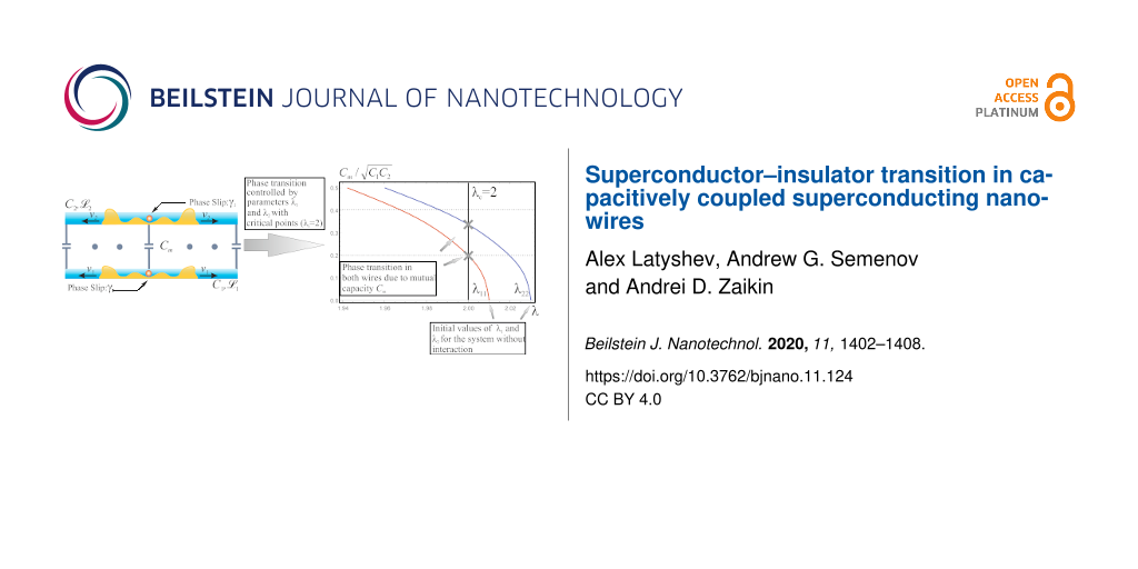
It is obvious that the strength of capacitive coupling depends on the distance between the wires. At large distances this coupling is negligible Cm → 0. However, as the wires get closer to each other the value Cm increases and, hence, their mutual influence increases as well. Let us choose the wire parameters in such a way that for Cm = 0 both these wires remain in the superconducting phase being relatively close to SIT. In this case the parameters λ1 and λ2 should be just slightly larger than 2. Moving the wires closer to each other we ”turn on” the capacitive coupling between them, thus, decreasing both values λ1 and λ2 to less than 2. As a result, two superconducting wires become insulating as soon as they are brought sufficiently close to each other. This remarkable physical phenomenon is illustrated by the phase diagram in Figure 2b.
![[2190-4286-11-124-2]](/bjnano/content/figures/2190-4286-11-124-2.png?scale=2.0&max-width=1024&background=FFFFFF)
Figure 2: a) Critical surfaces corresponding to SIT at λ11 = 2 and λ22 = 2. b) Phase diagram for two capacitively coupled superconducting nanowires with λ1 = 2.01 and λ2 = 2.03. Both curves λ11(Cm) and λ22(Cm) decrease and cross the critical line λc = 2 with increasing mutual capacitance, Cm.
Figure 2: a) Critical surfaces corresponding to SIT at λ11 = 2 and λ22 = 2. b) Phase diagram for two capaciti...
In order to complete this part of our analysis, we point out that transport properties can be investigated in exactly the same manner as was done in [5] in the case of a single nanowire. Generalization of the technique [5] to the case of two capacitively coupled superconducting nanowires is straightforward. For a linear resistance of the ith wire Ri(T) and for λii > 2 (or for any λii at sufficiently high temperatures) we obtain
![[2190-4286-11-124-i18]](/bjnano/content/inline/2190-4286-11-124-i18.svg?max-width=590&scale=1.18182)
Extension to other geometries
The effects discussed here can be observed in a variety of structures involving superconducting nanowires. For instance, superconducting nanowires in the form of a meander (see Figure 1b) are frequently employed in experiments [30]. In this case different segments of the wire are parallel to each other being close enough to develop electromagnetic coupling. Having in mind the above analysis, one expects that the wire of such a geometry would be ”less superconducting” than the same wire that has the form of a straight line.
For illustration, let us mimic the behavior of the wire depicted in Figure 1b by considering three identical capacitively coupled superconducting nanowires parallel to each other. For simplicity we will assume the nearest neighbor interaction, that is, the second (central) nanowire is coupled to both the first and the third nanowires via the mutual capacitance, Cm, whereas the latter two are decoupled from each other. We again assume that the wires are thin enough and quantum phase slips may proliferate in each of these wires.
The quantum properties of this system are described by the same effective action (Equation 11) where the inductance and capacitance matrices now take the form
![[2190-4286-11-124-i19]](/bjnano/content/inline/2190-4286-11-124-i19.svg?max-width=590&scale=1.18182)
and the summation runs over the indices i,j = 1,2,3. Proceeding along the same lines as in the previous section we again arrive at Equation 14, where the diagonal elements of the matrix ![[Graphic 26]](/bjnano/content/inline/2190-4286-11-124-i48.svg?max-width=637&scale=1.18182) now read
now read
![[2190-4286-11-124-i20]](/bjnano/content/inline/2190-4286-11-124-i20.svg?max-width=590&scale=1.18182)
![[2190-4286-11-124-i21]](/bjnano/content/inline/2190-4286-11-124-i21.svg?max-width=590&scale=1.18182)
and the QPS interaction parameter λ is defined in Equation 9. We again arrive at the RG equations of the form (Equation 16) (now with i = 1,2,3). Being combined with Equation 20 and Equation 21 these RG equations demonstrate that in the presence of capacitive coupling SETs occur at λii = 2 implying λ > 2 for each of the three wires. This observation is fully consistent with our previous results derived for two coupled nanowires.
Furthermore, the RG equation (Equation 16) with i = 2 combined with Equation 20 also describes the effect of interacting quantum phase slips and QPTs in the wire having the form of a meander (Figure 1b). In this case, within the approximation of the nearest neighbor, capacitive interaction between the wire segments QPT occurs at
![[2190-4286-11-124-i22]](/bjnano/content/inline/2190-4286-11-124-i22.svg?max-width=590&scale=1.18182)
that is, the critical value of the parameter λ exceeds 2 as soon as the mutual capacitance Cm differs from zero. As it is clear from Equation 20 and Equation 21, the approximation of the nearest neighbor interaction appears to be well justified in the limit Cm ≪ C. For stronger interactions with Cm ≈ C this approximation most likely becomes insufficient for a quantitative analysis. However, on a qualitative level our key observations should hold also in this case: A nanowire in the form of a straight line with λ slightly exceeding the critical value 2 should demonstrate superconducting-like behavior with R(T) ∝ T2λ−3 [5] whereas a wire with exactly the same parameters may turn insulating provided it has the form of a meander with capacitive coupling between its segments.
Conclusion
We have analyzed the effect of quantum fluctuations in capacitively coupled superconducting nanowires. We have demonstrated that plasma modes propagating in one such nanowire play the role of an effective quantum environment for another one, modifying the logarithmic interaction between quantum phase slips in this wire. As a result, the superconductor–insulator quantum phase transition gets shifted in a way to increase the parameter range for the insulating phase. Hence, superconducting nanowires may turn insulating provided they are brought close enough to each other. It would be interesting to observe this effect in forthcoming experiments with superconducting nanowires.
References
-
Zaikin, A. D.; Golubev, D. S. Dissipative Quantum Mechanics of Nanostructures: Electron Transport, Fluctuations and Interactions; Jenny Stanford Publishing: New York, NY, USA, 2019. doi:10.1201/9780429298233
Return to citation in text: [1] -
Arutyunov, K. Y.; Golubev, D. S.; Zaikin, A. D. Phys. Rep. 2008, 464, 1–70. doi:10.1016/j.physrep.2008.04.009
Return to citation in text: [1] -
Larkin, A. I.; Varlamov, A. A. Theory of fluctuations in superconductors; Clarendon: Oxford, U.K., 2005.
Return to citation in text: [1] -
Bezryadin, A. Superconductivity in Nanowires; Wiley-VCH: Weinheim, Germany, 2013. doi:10.1002/9783527651931
Return to citation in text: [1] -
Zaikin, A. D.; Golubev, D. S.; van Otterlo, A.; Zimányi, G. T. Phys. Rev. Lett. 1997, 78, 1552–1555. doi:10.1103/physrevlett.78.1552
Return to citation in text: [1] [2] [3] [4] [5] [6] [7] [8] [9] [10] [11] -
Golubev, D. S.; Zaikin, A. D. Phys. Rev. B 2001, 64, 014504. doi:10.1103/physrevb.64.014504
Return to citation in text: [1] [2] -
Bezryadin, A.; Lau, C. N.; Tinkham, M. Nature 2000, 404, 971–974. doi:10.1038/35010060
Return to citation in text: [1] -
Lau, C. N.; Markovic, N.; Bockrath, M.; Bezryadin, A.; Tinkham, M. Phys. Rev. Lett. 2001, 87, 217003. doi:10.1103/physrevlett.87.217003
Return to citation in text: [1] -
Zgirski, M.; Riikonen, K.-P.; Touboltsev, V.; Arutyunov, K. Y. Phys. Rev. B 2008, 77, 054508. doi:10.1103/physrevb.77.054508
Return to citation in text: [1] -
Baumans, X. D. A.; Cerbu, D.; Adami, O.-A.; Zharinov, V. S.; Verellen, N.; Papari, G.; Scheerder, J. E.; Zhang, G.; Moshchalkov, V. V.; Silhanek, A. V.; Van de Vondel, J. Nat. Commun. 2016, 7, 10560. doi:10.1038/ncomms10560
Return to citation in text: [1] -
Semenov, A. G.; Zaikin, A. D. Phys. Rev. B 2016, 94, 014512. doi:10.1103/physrevb.94.014512
Return to citation in text: [1] -
Semenov, A. G.; Zaikin, A. D. Phys. Rev. B 2019, 99, 094516. doi:10.1103/physrevb.99.094516
Return to citation in text: [1] -
Mooij, J. E.; Harmans, C. J. P. M. New J. Phys. 2005, 7, 219. doi:10.1088/1367-2630/7/1/219
Return to citation in text: [1] -
Semenov, A. G.; Zaikin, A. D. Phys. Rev. B 2013, 88, 054505. doi:10.1103/physrevb.88.054505
Return to citation in text: [1] [2] [3] -
Astafiev, O. V.; Ioffe, L. B.; Kafanov, S.; Pashkin, Y. A.; Arutyunov, K. Y.; Shahar, D.; Cohen, O.; Tsai, J. S. Nature 2012, 484, 355–358. doi:10.1038/nature10930
Return to citation in text: [1] -
de Graaf, S. E.; Skacel, S. T.; Hönigl-Decrinis, T.; Shaikhaidarov, R.; Rotzinger, H.; Linzen, S.; Ziegler, M.; Hübner, U.; Meyer, H.-G.; Antonov, V.; Il’ichev, E.; Ustinov, A. V.; Tzalenchuk, A. Y.; Astafiev, O. V. Nat. Phys. 2018, 14, 590–594. doi:10.1038/s41567-018-0097-9
Return to citation in text: [1] -
Mooij, J. E.; Schön, G. Phys. Rev. Lett. 1985, 55, 114–117. doi:10.1103/physrevlett.55.114
Return to citation in text: [1] -
Latyshev, A.; Semenov, A. G.; Zaikin, A. D. J. Supercond. Novel Magn. 2020, 33, 2329–2334. doi:10.1007/s10948-019-05402-3
Return to citation in text: [1] -
Schön, G.; Zaikin, A. D. Phys. Rep. 1990, 198, 237–412. doi:10.1016/0370-1573(90)90156-v
Return to citation in text: [1] [2] -
Guinea, F.; Schön, G. Europhys. Lett. 1986, 1, 585–593. doi:10.1209/0295-5075/1/11/007
Return to citation in text: [1] -
Panyukov, S. V.; Zaikin, A. D. Phys. Rev. Lett. 1991, 67, 3168–3171. doi:10.1103/physrevlett.67.3168
Return to citation in text: [1] -
Hofstetter, W.; Zwerger, W. Phys. Rev. Lett. 1997, 78, 3737–3740. doi:10.1103/physrevlett.78.3737
Return to citation in text: [1] -
Kindermann, M.; Nazarov, Y. V. Phys. Rev. Lett. 2003, 91, 136802. doi:10.1103/physrevlett.91.136802
Return to citation in text: [1] -
Golubev, D. S.; Zaikin, A. D. Phys. Rev. B 2004, 69, 075318. doi:10.1103/physrevb.69.075318
Return to citation in text: [1] -
Bagrets, D. A.; Nazarov, Y. V. Phys. Rev. Lett. 2005, 94, 056801. doi:10.1103/physrevlett.94.056801
Return to citation in text: [1] -
Schmid, A. Phys. Rev. Lett. 1983, 51, 1506–1509. doi:10.1103/physrevlett.51.1506
Return to citation in text: [1] -
Bulgadaev, S. A. JETP Lett. 1984, 39, 315–319.
Return to citation in text: [1] -
Guinea, F.; Hakim, V.; Muramatsu, A. Phys. Rev. Lett. 1985, 54, 263–266. doi:10.1103/physrevlett.54.263
Return to citation in text: [1] -
Kosterlitz, J. M. J. Phys. C 1974, 7, 1046–1060. doi:10.1088/0022-3719/7/6/005
Return to citation in text: [1] [2] -
Delacour, C.; Pannetier, B.; Villegier, J.-C.; Bouchiat, V. Nano Lett. 2012, 12, 3501–3506. doi:10.1021/nl3010397
Return to citation in text: [1]
| 30. | Delacour, C.; Pannetier, B.; Villegier, J.-C.; Bouchiat, V. Nano Lett. 2012, 12, 3501–3506. doi:10.1021/nl3010397 |
| 5. | Zaikin, A. D.; Golubev, D. S.; van Otterlo, A.; Zimányi, G. T. Phys. Rev. Lett. 1997, 78, 1552–1555. doi:10.1103/physrevlett.78.1552 |
| 1. | Zaikin, A. D.; Golubev, D. S. Dissipative Quantum Mechanics of Nanostructures: Electron Transport, Fluctuations and Interactions; Jenny Stanford Publishing: New York, NY, USA, 2019. doi:10.1201/9780429298233 |
| 2. | Arutyunov, K. Y.; Golubev, D. S.; Zaikin, A. D. Phys. Rep. 2008, 464, 1–70. doi:10.1016/j.physrep.2008.04.009 |
| 3. | Larkin, A. I.; Varlamov, A. A. Theory of fluctuations in superconductors; Clarendon: Oxford, U.K., 2005. |
| 4. | Bezryadin, A. Superconductivity in Nanowires; Wiley-VCH: Weinheim, Germany, 2013. doi:10.1002/9783527651931 |
| 12. | Semenov, A. G.; Zaikin, A. D. Phys. Rev. B 2019, 99, 094516. doi:10.1103/physrevb.99.094516 |
| 6. | Golubev, D. S.; Zaikin, A. D. Phys. Rev. B 2001, 64, 014504. doi:10.1103/physrevb.64.014504 |
| 11. | Semenov, A. G.; Zaikin, A. D. Phys. Rev. B 2016, 94, 014512. doi:10.1103/physrevb.94.014512 |
| 19. | Schön, G.; Zaikin, A. D. Phys. Rep. 1990, 198, 237–412. doi:10.1016/0370-1573(90)90156-v |
| 20. | Guinea, F.; Schön, G. Europhys. Lett. 1986, 1, 585–593. doi:10.1209/0295-5075/1/11/007 |
| 21. | Panyukov, S. V.; Zaikin, A. D. Phys. Rev. Lett. 1991, 67, 3168–3171. doi:10.1103/physrevlett.67.3168 |
| 22. | Hofstetter, W.; Zwerger, W. Phys. Rev. Lett. 1997, 78, 3737–3740. doi:10.1103/physrevlett.78.3737 |
| 7. | Bezryadin, A.; Lau, C. N.; Tinkham, M. Nature 2000, 404, 971–974. doi:10.1038/35010060 |
| 8. | Lau, C. N.; Markovic, N.; Bockrath, M.; Bezryadin, A.; Tinkham, M. Phys. Rev. Lett. 2001, 87, 217003. doi:10.1103/physrevlett.87.217003 |
| 9. | Zgirski, M.; Riikonen, K.-P.; Touboltsev, V.; Arutyunov, K. Y. Phys. Rev. B 2008, 77, 054508. doi:10.1103/physrevb.77.054508 |
| 10. | Baumans, X. D. A.; Cerbu, D.; Adami, O.-A.; Zharinov, V. S.; Verellen, N.; Papari, G.; Scheerder, J. E.; Zhang, G.; Moshchalkov, V. V.; Silhanek, A. V.; Van de Vondel, J. Nat. Commun. 2016, 7, 10560. doi:10.1038/ncomms10560 |
| 14. | Semenov, A. G.; Zaikin, A. D. Phys. Rev. B 2013, 88, 054505. doi:10.1103/physrevb.88.054505 |
| 5. | Zaikin, A. D.; Golubev, D. S.; van Otterlo, A.; Zimányi, G. T. Phys. Rev. Lett. 1997, 78, 1552–1555. doi:10.1103/physrevlett.78.1552 |
| 6. | Golubev, D. S.; Zaikin, A. D. Phys. Rev. B 2001, 64, 014504. doi:10.1103/physrevb.64.014504 |
| 14. | Semenov, A. G.; Zaikin, A. D. Phys. Rev. B 2013, 88, 054505. doi:10.1103/physrevb.88.054505 |
| 17. | Mooij, J. E.; Schön, G. Phys. Rev. Lett. 1985, 55, 114–117. doi:10.1103/physrevlett.55.114 |
| 5. | Zaikin, A. D.; Golubev, D. S.; van Otterlo, A.; Zimányi, G. T. Phys. Rev. Lett. 1997, 78, 1552–1555. doi:10.1103/physrevlett.78.1552 |
| 15. | Astafiev, O. V.; Ioffe, L. B.; Kafanov, S.; Pashkin, Y. A.; Arutyunov, K. Y.; Shahar, D.; Cohen, O.; Tsai, J. S. Nature 2012, 484, 355–358. doi:10.1038/nature10930 |
| 16. | de Graaf, S. E.; Skacel, S. T.; Hönigl-Decrinis, T.; Shaikhaidarov, R.; Rotzinger, H.; Linzen, S.; Ziegler, M.; Hübner, U.; Meyer, H.-G.; Antonov, V.; Il’ichev, E.; Ustinov, A. V.; Tzalenchuk, A. Y.; Astafiev, O. V. Nat. Phys. 2018, 14, 590–594. doi:10.1038/s41567-018-0097-9 |
| 18. | Latyshev, A.; Semenov, A. G.; Zaikin, A. D. J. Supercond. Novel Magn. 2020, 33, 2329–2334. doi:10.1007/s10948-019-05402-3 |
| 14. | Semenov, A. G.; Zaikin, A. D. Phys. Rev. B 2013, 88, 054505. doi:10.1103/physrevb.88.054505 |
| 13. | Mooij, J. E.; Harmans, C. J. P. M. New J. Phys. 2005, 7, 219. doi:10.1088/1367-2630/7/1/219 |
| 5. | Zaikin, A. D.; Golubev, D. S.; van Otterlo, A.; Zimányi, G. T. Phys. Rev. Lett. 1997, 78, 1552–1555. doi:10.1103/physrevlett.78.1552 |
| 5. | Zaikin, A. D.; Golubev, D. S.; van Otterlo, A.; Zimányi, G. T. Phys. Rev. Lett. 1997, 78, 1552–1555. doi:10.1103/physrevlett.78.1552 |
| 23. | Kindermann, M.; Nazarov, Y. V. Phys. Rev. Lett. 2003, 91, 136802. doi:10.1103/physrevlett.91.136802 |
| 24. | Golubev, D. S.; Zaikin, A. D. Phys. Rev. B 2004, 69, 075318. doi:10.1103/physrevb.69.075318 |
| 25. | Bagrets, D. A.; Nazarov, Y. V. Phys. Rev. Lett. 2005, 94, 056801. doi:10.1103/physrevlett.94.056801 |
| 19. | Schön, G.; Zaikin, A. D. Phys. Rep. 1990, 198, 237–412. doi:10.1016/0370-1573(90)90156-v |
| 26. | Schmid, A. Phys. Rev. Lett. 1983, 51, 1506–1509. doi:10.1103/physrevlett.51.1506 |
| 27. | Bulgadaev, S. A. JETP Lett. 1984, 39, 315–319. |
| 28. | Guinea, F.; Hakim, V.; Muramatsu, A. Phys. Rev. Lett. 1985, 54, 263–266. doi:10.1103/physrevlett.54.263 |
| 5. | Zaikin, A. D.; Golubev, D. S.; van Otterlo, A.; Zimányi, G. T. Phys. Rev. Lett. 1997, 78, 1552–1555. doi:10.1103/physrevlett.78.1552 |
| 5. | Zaikin, A. D.; Golubev, D. S.; van Otterlo, A.; Zimányi, G. T. Phys. Rev. Lett. 1997, 78, 1552–1555. doi:10.1103/physrevlett.78.1552 |
| 29. | Kosterlitz, J. M. J. Phys. C 1974, 7, 1046–1060. doi:10.1088/0022-3719/7/6/005 |
| 5. | Zaikin, A. D.; Golubev, D. S.; van Otterlo, A.; Zimányi, G. T. Phys. Rev. Lett. 1997, 78, 1552–1555. doi:10.1103/physrevlett.78.1552 |
| 5. | Zaikin, A. D.; Golubev, D. S.; van Otterlo, A.; Zimányi, G. T. Phys. Rev. Lett. 1997, 78, 1552–1555. doi:10.1103/physrevlett.78.1552 |
| 5. | Zaikin, A. D.; Golubev, D. S.; van Otterlo, A.; Zimányi, G. T. Phys. Rev. Lett. 1997, 78, 1552–1555. doi:10.1103/physrevlett.78.1552 |
| 29. | Kosterlitz, J. M. J. Phys. C 1974, 7, 1046–1060. doi:10.1088/0022-3719/7/6/005 |
| 5. | Zaikin, A. D.; Golubev, D. S.; van Otterlo, A.; Zimányi, G. T. Phys. Rev. Lett. 1997, 78, 1552–1555. doi:10.1103/physrevlett.78.1552 |
© 2020 Latyshev et al.; licensee Beilstein-Institut.
This is an Open Access article under the terms of the Creative Commons Attribution License (https://creativecommons.org/licenses/by/4.0). Please note that the reuse, redistribution and reproduction in particular requires that the authors and source are credited.
The license is subject to the Beilstein Journal of Nanotechnology terms and conditions: (https://www.beilstein-journals.org/bjnano)