Abstract
Electrons in two different normal metallic electrodes attached to a sufficiently thin superconducting island may become entangled due to the effect of Cooper pair splitting. This phenomenon is of fundamental importance and may also have serious implications for developing quantum communication technologies. One way to identify Cooper pair splitting is to analyze long-range cross correlations of fluctuating currents in three-terminal hybrid normal–superconducting–normal nanostructures. Here, we theoretically investigate non-trivial behavior of cross-correlated non-local shot noise in the presence of a temperature gradient. We suggest that applying a temperature gradient may serve as an extra tool to control the phenomenon of Cooper pair splitting.
Introduction
Normal metals connected to a superconductor exhibit a variety of non-trivial phenomena associated with the existence of proximity-induced superconducting correlations spreading over long distances at sufficiently low temperatures [1]. One of these phenomena is the so-called crossed Andreev reflection (CAR): A Cooper pair may split into two electrons [2] (see Figure 1a), thereby generating pairs of entangled electrons in different metallic electrodes [3]. This phenomenon and its effect on electron transport in normal metal–superconductor–normal metal (NSN) hybrid structures were intensively investigated both theoretically [4-10] and experimentally [11-18] over the past decades.
![[2190-4286-14-7-1]](/bjnano/content/figures/2190-4286-14-7-1.png?scale=2.0&max-width=1024&background=FFFFFF)
Figure 1: Schematics of the processes of crossed Andreev reflection (a) and elastic cotunneling (b). These schemes are redrawn from [25].
Figure 1: Schematics of the processes of crossed Andreev reflection (a) and elastic cotunneling (b). These sc...
The process competing with CAR is the so-called elastic cotunneling (EC), where an electron is transferred from one normal metal to another across an effective barrier created by the energy gap inside the superconductor, see Figure 1b. Unlike CAR, EC does not produce entangled electrons. In the zero-temperature limit, CAR and EC contributions to the low-bias non-local conductance of an NSN device cancel each other in the limit of low-transparency barriers [4]. In contrast, at high transmissions, the CAR contribution vanishes [6,7]. These observations make an unambiguous identification of CAR in transport experiments a non-trivial task.
The way out is to investigate fluctuations of electric currents passing through both NS boundaries of an NSN structure. While in non-superconducting multiterminal structures cross correlations of current noise in different terminals always remain negative [19], such cross correlations may become positive in the presence of superconductivity due to the process of CAR. This conclusion was initially reached theoretically in the limit of low-transparency barriers at NS interfaces [20,21] and later extended to the case of arbitrary barrier transmissions [22-25]. Positively cross-correlated non-local shot noise was indeed observed in a number of experiments [26,27]. Real-time observation of Cooper pair splitting was also reported in a recent work [28].
Usually, an interplay between positive and negative cross correlations of current noise in NSN devices can be controlled and tuned by applying external bias voltages. In this work we suggest another way of controlling Cooper pair splitting: We predict and investigate non-trivial behavior of cross-correlated non-local shot noise in the presence of a temperature gradient. Note that, previously, this so-called “delta-T” noise was studied in normal atomic-scale junctions [29]. Here, we demonstrate that such kind of noise can also manifest itself in subtle non-local properties of hybrid NSN structures associated with the phenomena of crossed Andreev reflection and Cooper pair splitting.
Results and Discussion
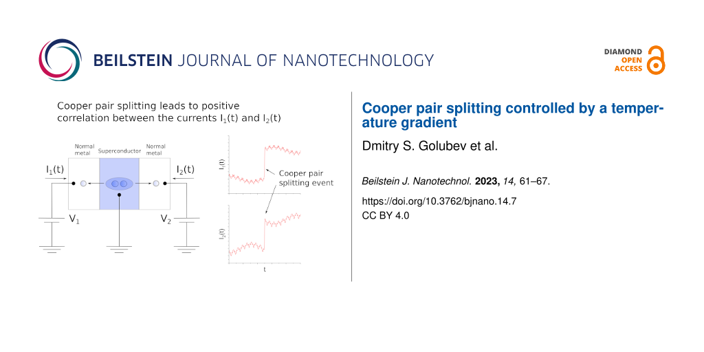
Let us consider the NSN structure depicted in Figure 2. Normal metallic leads are attached to a bulk superconductor with the aid of two junctions described by a set of conducting channel transmissions τ1,n and τ2,n with n being the integer number enumerating all conducting channels. The two junctions are located at a distance considerably shorter than the superconducting coherence length ξ. Normal electrodes are kept at different temperatures T1 and T2, thus creating a temperature gradient across our device. In addition, voltages V1 and V2 can be applied to two normal leads, as shown in Figure 2.
![[2190-4286-14-7-2]](/bjnano/content/figures/2190-4286-14-7-2.png?scale=2.0&max-width=1024&background=FFFFFF)
Figure 2: Schematics of the NSN structure under consideration. Normal electrodes are biased by external voltages V1 and V2 and are kept at different temperatures T1 and T2. The superconducting electrode is assumed to be thinner than the superconducting coherence length ξ.
Figure 2: Schematics of the NSN structure under consideration. Normal electrodes are biased by external volta...
The Hamiltonian of this structure can be chosen in the form
![[2190-4286-14-7-i1]](/bjnano/content/inline/2190-4286-14-7-i1.svg?max-width=590&scale=1.18182)
where
![[2190-4286-14-7-i2]](/bjnano/content/inline/2190-4286-14-7-i2.svg?max-width=590&scale=1.18182)
are the Hamiltonians of two normal leads, ![[Graphic 1]](/bjnano/content/inline/2190-4286-14-7-i30.svg?max-width=637&scale=1.18182) denote creation and annihilation operators for an electron with a spin projection α at a point x, m is the electron mass, and μ is the chemical potential,
denote creation and annihilation operators for an electron with a spin projection α at a point x, m is the electron mass, and μ is the chemical potential,
![[2190-4286-14-7-i3]](/bjnano/content/inline/2190-4286-14-7-i3.svg?max-width=590&scale=1.18182)
is the Hamiltonian of a superconducting electrode with the order parameter Δ and the terms
![[2190-4286-14-7-i4]](/bjnano/content/inline/2190-4286-14-7-i4.svg?max-width=590&scale=1.18182)
account for electron transfer through the junctions between the superconductor and the normal leads. In Equation 4, the surface integrals are taken over the contact areas ![[Graphic 2]](/bjnano/content/inline/2190-4286-14-7-i31.svg?max-width=637&scale=1.18182) , and tr(x) denote coordinate- and spin-independent tunneling amplitudes.
, and tr(x) denote coordinate- and spin-independent tunneling amplitudes.
Let us denote the probability for N1 and N2 electrons to be transferred, respectively, through the junctions 1 and 2 during the observation time t as Pt(N1,N2). Introducing the so-called cumulant generating function ![[Graphic 3]](/bjnano/content/inline/2190-4286-14-7-i32.svg?max-width=637&scale=1.18182) (χ1,χ2) by means of the formula
(χ1,χ2) by means of the formula
![[2190-4286-14-7-i5]](/bjnano/content/inline/2190-4286-14-7-i5.svg?max-width=590&scale=1.18182)
with χ1,2 being the counting fields, one can express the average currents through the junctions ![[Graphic 4]](/bjnano/content/inline/2190-4286-14-7-i33.svg?max-width=637&scale=1.18182) , and the current–current correlation functions
, and the current–current correlation functions
![[2190-4286-14-7-i6]](/bjnano/content/inline/2190-4286-14-7-i6.svg?max-width=590&scale=1.18182)
in the following form
![[2190-4286-14-7-i7]](/bjnano/content/inline/2190-4286-14-7-i7.svg?max-width=590&scale=1.18182)
The cumulant generating function ![[Graphic 5]](/bjnano/content/inline/2190-4286-14-7-i34.svg?max-width=637&scale=1.18182) in Equation 5 be evaluated in a general form with the aid of the path integral technique [22,25], which yields
in Equation 5 be evaluated in a general form with the aid of the path integral technique [22,25], which yields
![[2190-4286-14-7-i8]](/bjnano/content/inline/2190-4286-14-7-i8.svg?max-width=590&scale=1.18182)
where ![[Graphic 6]](/bjnano/content/inline/2190-4286-14-7-i35.svg?max-width=637&scale=1.18182) is the Keldysh Green function of our system
is the Keldysh Green function of our system
![[2190-4286-14-7-i9]](/bjnano/content/inline/2190-4286-14-7-i9.svg?max-width=590&scale=1.18182)
the 4 × 4 matrices ![[Graphic 7]](/bjnano/content/inline/2190-4286-14-7-i36.svg?max-width=637&scale=1.18182) represent the inverse Keldysh Green functions of isolated normal and superconducting leads and
represent the inverse Keldysh Green functions of isolated normal and superconducting leads and ![[Graphic 8]](/bjnano/content/inline/2190-4286-14-7-i37.svg?max-width=637&scale=1.18182) is the diagonal 4 × 4 matrix in the Nambu–Keldysh space describing tunneling between the leads,
is the diagonal 4 × 4 matrix in the Nambu–Keldysh space describing tunneling between the leads,
![[2190-4286-14-7-i10]](/bjnano/content/inline/2190-4286-14-7-i10.svg?max-width=590&scale=1.18182)
Further analysis of the general expression for the function ![[Graphic 9]](/bjnano/content/inline/2190-4286-14-7-i38.svg?max-width=637&scale=1.18182) (Equation 8) is essentially identical to that already carried out in [25]. Therefore, it is not necessary to go into details here. Employing Equation 7 and making use of the results [25], we recover general expressions for both the currents Ir across the junctions and the cross-correlated current noise S12 in the presence of a temperature gradient between two normal terminals.
(Equation 8) is essentially identical to that already carried out in [25]. Therefore, it is not necessary to go into details here. Employing Equation 7 and making use of the results [25], we recover general expressions for both the currents Ir across the junctions and the cross-correlated current noise S12 in the presence of a temperature gradient between two normal terminals.
In what follows we will be particularly interested in the limit of low voltages and temperatures eV1,2,T1,2 ≪ Δ. In this case, Ir (containing both local and non-local components) is practically insensitive to temperature and matches with the results [6,7,10] derived earlier in the corresponding limit.
For the non-local current noise in the same limit eV1,2,T1,2 ≪ Δ we obtain
![[2190-4286-14-7-i11]](/bjnano/content/inline/2190-4286-14-7-i11.svg?max-width=590&scale=1.18182)
where we defined the Andreev reflection probabilities per conducting channel in both junctions
![[2190-4286-14-7-i12]](/bjnano/content/inline/2190-4286-14-7-i12.svg?max-width=590&scale=1.18182)
introduced the function
![[2190-4286-14-7-i13]](/bjnano/content/inline/2190-4286-14-7-i13.svg?max-width=590&scale=1.18182)
and employed Fermi distribution functions for electrons and holes in the normal leads
![[2190-4286-14-7-i14]](/bjnano/content/inline/2190-4286-14-7-i14.svg?max-width=590&scale=1.18182)
Equation 11 defines the low-energy cross-correlated current noise in the presence of a temperature gradient and represents the main general result of the present work.
The expression (Equation 11) contains the integrals of the type ![[Graphic 10]](/bjnano/content/inline/2190-4286-14-7-i39.svg?max-width=637&scale=1.18182) , which cannot be handled analytically except in some special limits, i.e.,
, which cannot be handled analytically except in some special limits, i.e.,
![[2190-4286-14-7-i15]](/bjnano/content/inline/2190-4286-14-7-i15.svg?max-width=590&scale=1.18182)
for T1 = T2 = T and
![[2190-4286-14-7-i16]](/bjnano/content/inline/2190-4286-14-7-i16.svg?max-width=590&scale=1.18182)
for T1 ≫ T2. In the opposite limit T2 ≫ T1 in Equation 16 one should simply interchange T1 ↔ T2.
In order to proceed, we note that there exists a very accurate interpolation formula between the above limits. It reads
![[2190-4286-14-7-i17]](/bjnano/content/inline/2190-4286-14-7-i17.svg?max-width=590&scale=1.18182)
where we defined an effective temperature
![[2190-4286-14-7-i18]](/bjnano/content/inline/2190-4286-14-7-i18.svg?max-width=590&scale=1.18182)
and introduced the notations T = (T1 + T2)/2 and δT = T1 − T2.
With the aid of this interpolation, the non-local noise (Equation 11) can be reduced to a much simpler form
![[2190-4286-14-7-i19]](/bjnano/content/inline/2190-4286-14-7-i19.svg?max-width=590&scale=1.18182)
Here we have introduced the non-local conductance in the limit of zero temperature and zero bias voltage,
![[2190-4286-14-7-i20]](/bjnano/content/inline/2190-4286-14-7-i20.svg?max-width=590&scale=1.18182)
![[Graphic 11]](/bjnano/content/inline/2190-4286-14-7-i40.svg?max-width=637&scale=1.18182) being the normal state resistance of a superconducting island [25], as well as the parameters
being the normal state resistance of a superconducting island [25], as well as the parameters
![[2190-4286-14-7-i21]](/bjnano/content/inline/2190-4286-14-7-i21.svg?max-width=590&scale=1.18182)
and the local Fano factors for two barriers in the Andreev reflection regime
![[2190-4286-14-7-i22]](/bjnano/content/inline/2190-4286-14-7-i22.svg?max-width=590&scale=1.18182)
At zero bias voltages V1 = V2 = 0, we obtain the noise in the form
![[2190-4286-14-7-i23]](/bjnano/content/inline/2190-4286-14-7-i23.svg?max-width=590&scale=1.18182)
Hence, for the excess non-local noise δS12 = S12(T,δT) − S12(T,0) induced by the temperature gradient we get
![[2190-4286-14-7-i24]](/bjnano/content/inline/2190-4286-14-7-i24.svg?max-width=590&scale=1.18182)
This contribution is positive and reaches its maximum δS12 ≃ 0.44G12T at |δT| = T.
The effect of the temperature gradient on cross-correlated non-local noise remains appreciable also at non-zero bias voltages V1,2, in which case it essentially depends on transmission distributions in both junctions.
We start from the tunneling limit A1,n, A2,m ≪ 1, where one has
![[2190-4286-14-7-i25]](/bjnano/content/inline/2190-4286-14-7-i25.svg?max-width=590&scale=1.18182)
Keeping only the terms ∝γ± in the expression (Equation 19), we obtain
![[2190-4286-14-7-i26]](/bjnano/content/inline/2190-4286-14-7-i26.svg?max-width=590&scale=1.18182)
The first and the second terms on the right-hand side of this formula are attributed, respectively, to CAR and EC processes. We observe that, similarly to the limit δT = 0, the noise cross correlations remain positive, S12 > 0, provided V1 and V2 have the same sign, and they turn negative, S12 < 0, should V1 and V2 have different signs. The result is also illustrated in Figure 3.
![[2190-4286-14-7-3]](/bjnano/content/figures/2190-4286-14-7-3.png?scale=2.0&max-width=1024&background=FFFFFF)
Figure 3: Non-local noise S12 (Equation 26) in the tunneling limit (Equation 25). Left panel: T = 0; middle panel: T = 0.1Δ, δT = 0; right panel: |δT| = T = 0.1Δ.
Figure 3: Non-local noise S12 (Equation 26) in the tunneling limit (Equation 25). Left panel: T = 0; middle panel: T = 0.1Δ, δT = 0...
In the opposite limit of perfectly conducting channels in both junctions with τ1,n = τ2,m = 1 one gets γ+ = 2, γ− = 0, β1 = β2 = 0. Hence, in this case, Equation 19 yields
![[2190-4286-14-7-i27]](/bjnano/content/inline/2190-4286-14-7-i27.svg?max-width=590&scale=1.18182)
This result is always positive at non-zero bias and sufficiently low temperatures, indicating the importance of CAR processes in this limit, see also Figure 4.
![[2190-4286-14-7-4]](/bjnano/content/figures/2190-4286-14-7-4.png?scale=2.0&max-width=1024&background=FFFFFF)
Figure 4: Non-local noise S12 (Equation 27) in the case of fully transparent junctions. Left panel: T = 0; middle panel: T = 0.05Δ, δT = 0; right panel: |δT| = T = 0.05Δ.
Figure 4: Non-local noise S12 (Equation 27) in the case of fully transparent junctions. Left panel: T = 0; middle panel: ...
Yet another important physical limit is realized provided the contact has the form of a short diffusive wire with the corresponding Thouless energy exceeding the superconducting gap Δ. In this diffusive limit the transmission probability distributions in both junctions are defined by the well-known formula
![[2190-4286-14-7-i28]](/bjnano/content/inline/2190-4286-14-7-i28.svg?max-width=590&scale=1.18182)
with ![[Graphic 12]](/bjnano/content/inline/2190-4286-14-7-i41.svg?max-width=637&scale=1.18182) being the resistances of diffusive contacts in the normal state. Making use of this formula, one readily finds γ± = ±1 and β1 = β2 = 1/3. Then Equation 19 reduces to
being the resistances of diffusive contacts in the normal state. Making use of this formula, one readily finds γ± = ±1 and β1 = β2 = 1/3. Then Equation 19 reduces to
![[2190-4286-14-7-i29]](/bjnano/content/inline/2190-4286-14-7-i29.svg?max-width=590&scale=1.18182)
This result is also displayed in Figure 5.
![[2190-4286-14-7-5]](/bjnano/content/figures/2190-4286-14-7-5.png?scale=2.0&max-width=1024&background=FFFFFF)
Figure 5: Non-local noise S12 (Equation 29) in the case of diffusive barriers. Left panel: T = 0; middle panel: T = 0.03Δ, δT = 0; right panel: |δT| = T = 0.03Δ.
Figure 5: Non-local noise S12 (Equation 29) in the case of diffusive barriers. Left panel: T = 0; middle panel: T = 0.03...
Conclusion
Comparing the non-local shot noise pattern in all the above limits, we can make several important conclusions. First, in full accordance with our previous results [22,25], this pattern turns out to be markedly different depending on particular transmission distributions for intermetallic barriers, thus emphasizing different roles played by CAR and EC processes. Second, relative contributions of the latter processes can be reliably controlled by applied external bias voltages V1 and V2 as well as by varying temperature T. Third, we observe that the non-local shot noise patterns undergoes additional modifications provided a temperature gradient is applied to our structure. Hence, the temperature gradient, along with other parameters, can also serve as a possible extra tool to control and tune the process of Cooper pair splitting in multiterminal hybrid normal–superconducting metallic structures.
References
-
Belzig, W.; Wilhelm, F. K.; Bruder, C.; Schön, G.; Zaikin, A. D. Superlattices Microstruct. 1999, 25, 1251–1288. doi:10.1006/spmi.1999.0710
Return to citation in text: [1] -
Deutscher, G.; Feinberg, D. Appl. Phys. Lett. 2000, 76, 487–489. doi:10.1063/1.125796
Return to citation in text: [1] -
Lesovik, G. B.; Martin, T.; Blatter, G. Eur. Phys. J. B 2001, 24, 287–290. doi:10.1007/s10051-001-8675-4
Return to citation in text: [1] -
Falci, G.; Feinberg, D.; Hekking, F. W. J. Europhys. Lett. 2001, 54, 255–261. doi:10.1209/epl/i2001-00303-0
Return to citation in text: [1] [2] -
Brinkman, A.; Golubov, A. A. Phys. Rev. B 2006, 74, 214512. doi:10.1103/physrevb.74.214512
Return to citation in text: [1] -
Kalenkov, M. S.; Zaikin, A. D. Phys. Rev. B 2007, 75, 172503. doi:10.1103/physrevb.75.172503
Return to citation in text: [1] [2] [3] -
Kalenkov, M. S.; Zaikin, A. D. Phys. Rev. B 2007, 76, 224506. doi:10.1103/physrevb.76.224506
Return to citation in text: [1] [2] [3] -
Morten, J. P.; Brataas, A.; Belzig, W. Phys. Rev. B 2006, 74, 214510. doi:10.1103/physrevb.74.214510
Return to citation in text: [1] -
Golubev, D. S.; Zaikin, A. D. Phys. Rev. B 2007, 76, 184510. doi:10.1103/physrevb.76.184510
Return to citation in text: [1] -
Golubev, D. S.; Kalenkov, M. S.; Zaikin, A. D. Phys. Rev. Lett. 2009, 103, 067006. doi:10.1103/physrevlett.103.067006
Return to citation in text: [1] [2] -
Beckmann, D.; Weber, H. B.; v. Löhneysen, H. Phys. Rev. Lett. 2004, 93, 197003. doi:10.1103/physrevlett.93.197003
Return to citation in text: [1] -
Russo, S.; Kroug, M.; Klapwijk, T. M.; Morpurgo, A. F. Phys. Rev. Lett. 2005, 95, 027002. doi:10.1103/physrevlett.95.027002
Return to citation in text: [1] -
Cadden-Zimansky, P.; Chandrasekhar, V. Phys. Rev. Lett. 2006, 97, 237003. doi:10.1103/physrevlett.97.237003
Return to citation in text: [1] -
Hofstetter, L.; Csonka, S.; Nygård, J.; Schönenberger, C. Nature 2009, 461, 960–963. doi:10.1038/nature08432
Return to citation in text: [1] -
Kleine, A.; Baumgartner, A.; Trbovic, J.; Golubev, D. S.; Zaikin, A. D.; Schönenberger, C. Nanotechnology 2010, 21, 274002. doi:10.1088/0957-4484/21/27/274002
Return to citation in text: [1] -
Brauer, J.; Hübler, F.; Smetanin, M.; Beckmann, D.; v. Löhneysen, H. Phys. Rev. B 2010, 81, 024515. doi:10.1103/physrevb.81.024515
Return to citation in text: [1] -
Schindele, J.; Baumgartner, A.; Schönenberger, C. Phys. Rev. Lett. 2012, 109, 157002. doi:10.1103/physrevlett.109.157002
Return to citation in text: [1] -
Kolenda, S.; Wolf, M. J.; Golubev, D. S.; Zaikin, A. D.; Beckmann, D. Phys. Rev. B 2013, 88, 174509. doi:10.1103/physrevb.88.174509
Return to citation in text: [1] -
Blanter, Y. M.; Büttiker, M. Phys. Rep. 2000, 336, 1–166. doi:10.1016/s0370-1573(99)00123-4
Return to citation in text: [1] -
Börlin, J.; Belzig, W.; Bruder, C. Phys. Rev. Lett. 2002, 88, 197001. doi:10.1103/physrevlett.88.197001
Return to citation in text: [1] -
Bignon, G.; Houzet, M.; Pistolesi, F.; Hekking, F. W. J. Europhys. Lett. 2004, 67, 110–116. doi:10.1209/epl/i2003-10293-9
Return to citation in text: [1] -
Golubev, D. S.; Zaikin, A. D. Phys. Rev. B 2010, 82, 134508. doi:10.1103/physrevb.82.134508
Return to citation in text: [1] [2] [3] -
Freyn, A.; Flöser, M.; Mélin, R. Phys. Rev. B 2010, 82, 014510. doi:10.1103/physrevb.82.014510
Return to citation in text: [1] -
Flöser, M.; Feinberg, D.; Mélin, R. Phys. Rev. B 2013, 88, 094517. doi:10.1103/physrevb.88.094517
Return to citation in text: [1] -
Golubev, D. S.; Zaikin, A. D. Phys. Rev. B 2019, 99, 144504. doi:10.1103/physrevb.99.144504
Return to citation in text: [1] [2] [3] [4] [5] [6] [7] -
Wei, J.; Chandrasekhar, V. Nat. Phys. 2010, 6, 494–498. doi:10.1038/nphys1669
Return to citation in text: [1] -
Das, A.; Ronen, Y.; Heiblum, M.; Mahalu, D.; Kretinin, A. V.; Shtrikman, H. Nat. Commun. 2012, 3, 1165. doi:10.1038/ncomms2169
Return to citation in text: [1] -
Ranni, A.; Brange, F.; Mannila, E. T.; Flindt, C.; Maisi, V. F. Nat. Commun. 2021, 12, 6358. doi:10.1038/s41467-021-26627-8
Return to citation in text: [1] -
Lumbroso, O. S.; Simine, L.; Nitzan, A.; Segal, D.; Tal, O. Nature 2018, 562, 240–244. doi:10.1038/s41586-018-0592-2
Return to citation in text: [1]
| 25. | Golubev, D. S.; Zaikin, A. D. Phys. Rev. B 2019, 99, 144504. doi:10.1103/physrevb.99.144504 |
| 25. | Golubev, D. S.; Zaikin, A. D. Phys. Rev. B 2019, 99, 144504. doi:10.1103/physrevb.99.144504 |
| 6. | Kalenkov, M. S.; Zaikin, A. D. Phys. Rev. B 2007, 75, 172503. doi:10.1103/physrevb.75.172503 |
| 7. | Kalenkov, M. S.; Zaikin, A. D. Phys. Rev. B 2007, 76, 224506. doi:10.1103/physrevb.76.224506 |
| 10. | Golubev, D. S.; Kalenkov, M. S.; Zaikin, A. D. Phys. Rev. Lett. 2009, 103, 067006. doi:10.1103/physrevlett.103.067006 |
| 1. | Belzig, W.; Wilhelm, F. K.; Bruder, C.; Schön, G.; Zaikin, A. D. Superlattices Microstruct. 1999, 25, 1251–1288. doi:10.1006/spmi.1999.0710 |
| 11. | Beckmann, D.; Weber, H. B.; v. Löhneysen, H. Phys. Rev. Lett. 2004, 93, 197003. doi:10.1103/physrevlett.93.197003 |
| 12. | Russo, S.; Kroug, M.; Klapwijk, T. M.; Morpurgo, A. F. Phys. Rev. Lett. 2005, 95, 027002. doi:10.1103/physrevlett.95.027002 |
| 13. | Cadden-Zimansky, P.; Chandrasekhar, V. Phys. Rev. Lett. 2006, 97, 237003. doi:10.1103/physrevlett.97.237003 |
| 14. | Hofstetter, L.; Csonka, S.; Nygård, J.; Schönenberger, C. Nature 2009, 461, 960–963. doi:10.1038/nature08432 |
| 15. | Kleine, A.; Baumgartner, A.; Trbovic, J.; Golubev, D. S.; Zaikin, A. D.; Schönenberger, C. Nanotechnology 2010, 21, 274002. doi:10.1088/0957-4484/21/27/274002 |
| 16. | Brauer, J.; Hübler, F.; Smetanin, M.; Beckmann, D.; v. Löhneysen, H. Phys. Rev. B 2010, 81, 024515. doi:10.1103/physrevb.81.024515 |
| 17. | Schindele, J.; Baumgartner, A.; Schönenberger, C. Phys. Rev. Lett. 2012, 109, 157002. doi:10.1103/physrevlett.109.157002 |
| 18. | Kolenda, S.; Wolf, M. J.; Golubev, D. S.; Zaikin, A. D.; Beckmann, D. Phys. Rev. B 2013, 88, 174509. doi:10.1103/physrevb.88.174509 |
| 22. | Golubev, D. S.; Zaikin, A. D. Phys. Rev. B 2010, 82, 134508. doi:10.1103/physrevb.82.134508 |
| 25. | Golubev, D. S.; Zaikin, A. D. Phys. Rev. B 2019, 99, 144504. doi:10.1103/physrevb.99.144504 |
| 4. | Falci, G.; Feinberg, D.; Hekking, F. W. J. Europhys. Lett. 2001, 54, 255–261. doi:10.1209/epl/i2001-00303-0 |
| 5. | Brinkman, A.; Golubov, A. A. Phys. Rev. B 2006, 74, 214512. doi:10.1103/physrevb.74.214512 |
| 6. | Kalenkov, M. S.; Zaikin, A. D. Phys. Rev. B 2007, 75, 172503. doi:10.1103/physrevb.75.172503 |
| 7. | Kalenkov, M. S.; Zaikin, A. D. Phys. Rev. B 2007, 76, 224506. doi:10.1103/physrevb.76.224506 |
| 8. | Morten, J. P.; Brataas, A.; Belzig, W. Phys. Rev. B 2006, 74, 214510. doi:10.1103/physrevb.74.214510 |
| 9. | Golubev, D. S.; Zaikin, A. D. Phys. Rev. B 2007, 76, 184510. doi:10.1103/physrevb.76.184510 |
| 10. | Golubev, D. S.; Kalenkov, M. S.; Zaikin, A. D. Phys. Rev. Lett. 2009, 103, 067006. doi:10.1103/physrevlett.103.067006 |
| 25. | Golubev, D. S.; Zaikin, A. D. Phys. Rev. B 2019, 99, 144504. doi:10.1103/physrevb.99.144504 |
| 3. | Lesovik, G. B.; Martin, T.; Blatter, G. Eur. Phys. J. B 2001, 24, 287–290. doi:10.1007/s10051-001-8675-4 |
| 28. | Ranni, A.; Brange, F.; Mannila, E. T.; Flindt, C.; Maisi, V. F. Nat. Commun. 2021, 12, 6358. doi:10.1038/s41467-021-26627-8 |
| 2. | Deutscher, G.; Feinberg, D. Appl. Phys. Lett. 2000, 76, 487–489. doi:10.1063/1.125796 |
| 29. | Lumbroso, O. S.; Simine, L.; Nitzan, A.; Segal, D.; Tal, O. Nature 2018, 562, 240–244. doi:10.1038/s41586-018-0592-2 |
| 19. | Blanter, Y. M.; Büttiker, M. Phys. Rep. 2000, 336, 1–166. doi:10.1016/s0370-1573(99)00123-4 |
| 22. | Golubev, D. S.; Zaikin, A. D. Phys. Rev. B 2010, 82, 134508. doi:10.1103/physrevb.82.134508 |
| 23. | Freyn, A.; Flöser, M.; Mélin, R. Phys. Rev. B 2010, 82, 014510. doi:10.1103/physrevb.82.014510 |
| 24. | Flöser, M.; Feinberg, D.; Mélin, R. Phys. Rev. B 2013, 88, 094517. doi:10.1103/physrevb.88.094517 |
| 25. | Golubev, D. S.; Zaikin, A. D. Phys. Rev. B 2019, 99, 144504. doi:10.1103/physrevb.99.144504 |
| 6. | Kalenkov, M. S.; Zaikin, A. D. Phys. Rev. B 2007, 75, 172503. doi:10.1103/physrevb.75.172503 |
| 7. | Kalenkov, M. S.; Zaikin, A. D. Phys. Rev. B 2007, 76, 224506. doi:10.1103/physrevb.76.224506 |
| 26. | Wei, J.; Chandrasekhar, V. Nat. Phys. 2010, 6, 494–498. doi:10.1038/nphys1669 |
| 27. | Das, A.; Ronen, Y.; Heiblum, M.; Mahalu, D.; Kretinin, A. V.; Shtrikman, H. Nat. Commun. 2012, 3, 1165. doi:10.1038/ncomms2169 |
| 4. | Falci, G.; Feinberg, D.; Hekking, F. W. J. Europhys. Lett. 2001, 54, 255–261. doi:10.1209/epl/i2001-00303-0 |
| 22. | Golubev, D. S.; Zaikin, A. D. Phys. Rev. B 2010, 82, 134508. doi:10.1103/physrevb.82.134508 |
| 25. | Golubev, D. S.; Zaikin, A. D. Phys. Rev. B 2019, 99, 144504. doi:10.1103/physrevb.99.144504 |
| 25. | Golubev, D. S.; Zaikin, A. D. Phys. Rev. B 2019, 99, 144504. doi:10.1103/physrevb.99.144504 |
| 20. | Börlin, J.; Belzig, W.; Bruder, C. Phys. Rev. Lett. 2002, 88, 197001. doi:10.1103/physrevlett.88.197001 |
| 21. | Bignon, G.; Houzet, M.; Pistolesi, F.; Hekking, F. W. J. Europhys. Lett. 2004, 67, 110–116. doi:10.1209/epl/i2003-10293-9 |
© 2023 Golubev and Zaikin; licensee Beilstein-Institut.
This is an open access article licensed under the terms of the Beilstein-Institut Open Access License Agreement (https://www.beilstein-journals.org/bjnano/terms), which is identical to the Creative Commons Attribution 4.0 International License (https://creativecommons.org/licenses/by/4.0). The reuse of material under this license requires that the author(s), source and license are credited. Third-party material in this article could be subject to other licenses (typically indicated in the credit line), and in this case, users are required to obtain permission from the license holder to reuse the material.