Abstract
The aim of this work is to study the surface passivation of aluminum oxide/amorphous silicon carbide (Al2O3/a-SiCx) stacks on both p-type and n-type crystalline silicon (c-Si) substrates as well as the optical characterization of these stacks. Al2O3 films of different thicknesses were deposited by thermal atomic layer deposition (ALD) at 200 °C and were complemented with a layer of a-SiCx deposited by plasma-enhanced chemical vapor deposition (PECVD) to form anti-reflection coating (ARC) stacks with a total thickness of 75 nm. A comparative study has been carried out on polished and randomly textured wafers. We have experimentally determined the optimum thickness of the stack for photovoltaic applications by minimizing the reflection losses over a wide wavelength range (300–1200 nm) without compromising the outstanding passivation properties of the Al2O3 films. The upper limit of the surface recombination velocity (Seff,max) was evaluated at a carrier injection level corresponding to 1-sun illumination, which led to values below 10 cm/s. Reflectance values below 2% were measured on textured samples over the wavelength range of 450–1000 nm.
Introduction
Surface passivation has become a relevant issue in high efficiency crystalline silicon (c-Si) solar cells. The importance is even increasing as thinner wafers are used to reduce the cost for photovoltaic applications [1]. Aluminum oxide (Al2O3) grown by atomic layer deposition (ALD) is a good alternative for passivating both lightly and highly doped n- and also p-type c-Si substrates [2-4]. The excellent passivation quality is due to a double effect: (i) chemical passivation that involves a low density of interface defects, Dit (≈1011 eV−1cm−2), and (ii) field-effect passivation due to a high negative fixed-charge density, Qfix (≈1012 cm−2) [5-8], which acts as an electrostatic shielding and significantly reduces the density of one type of charge carrier at the interface c-Si/Al2O3 [9,10]. In order to achieve the lowest surface recombination velocity (Seff), it is necessary to perfom a thermal treatment after deposition (post-deposition annealing) to activate the passivating properties of Al2O3 layers [11,12]. In a previous work [13] we showed that an annealing process for 10 to 20 min at temperatures between 350 °C and 400 °C is enough to obtain an excellent passivation on polished p-type c-Si substrates.
In this work, we complement our preceding work by studying the surface recombination velocity on both n- and p-type wafers (polished and randomly textured), which were passivated with Al2O3/a-SiCx stacks. In previous works we demonstrated that an a-SiCx capping layer on the Al2O3 improves the laser contact formation on p-type c-Si solar cells in comparison to the typical laser fired contact (LFC) process [14,15]. Moreover, it is well known that the ALD deposition of Al2O3 has very low deposition rates. Inserting an a-SiCx capping layer by PECVD technique can overcome this drawback. In this study, we have investigated different combinations of layers that provide good antireflection properties while maintaining a total film thickness of 75 nm. In addition to the passivation, a high-quality antireflection coating (ARC) plays a vital role in highly efficient solar cells [16]. We have measured the reflectance over a wide wavelength range, 300–1200 nm, in order to determine the optimum layer thicknesses for the stack to be used as an ARC without compromising the surface passivation quality.
Results and Discussion
Surface recombination results
The passivation characteristics of the c-Si/Al2O3/a-SiCx stacks were tested the deposition of Al2O3 and a-SiCx, and after a final post-deposition annealing process (Figure 1). Moderate Seff,max values were achieved for as-deposited Al2O3 layers with better results on polished than on randomly textured samples. This level of surface passivation can be explained by the relatively low Dit (≈1011 eV−1cm−2) prior to the annealing step [17,18], which is responsible for the chemical passivation. The higher Seff,max results obtained on textured samples (>130 cm/s) could be attributed to a higher surface area due to the pyramid-shaped surface and a higher Dit value on the exposed {111} planes [19-21]. Regarding the field-effect passivation, it has been reported that ALD Al2O3 films exhibit a low Qfix present at the c-Si/Al2O3 interface (≈1011 cm−2) prior to the annealing step [18]. Under these conditions, the electrostatic shielding of the interface does not induce an increase of the τeff value and the effect of the chemical passivation becomes more determinant. After the a-SiCx deposition by PECVD, we observe in general a considerable improvement of the Seff,max parameter. Values close to 10 cm/s were achieved on polished n- and p-type samples. This effect can be attributed to a small in-situ annealing effect that takes place in the PECVD chamber (deposition temperature Tdep= 300 °C). The improvement of the passivation quality after an annealing step has been widely reported [3,7,18,22], and it has been related to a lower Dit ≤ 1 × 10¹¹ eV−1cm−2 [17] combined with a higher concentration of fixed negative charges. The presence of these charges provides an electrostatic shielding due to a built-in electric field at the c-Si/Al2O3 interface [4,23]. Here, we also see that textured substrates showed higher Seff values after the SiCx deposition.
![[2190-4286-4-82-1]](/bjnano/content/figures/2190-4286-4-82-1.svg?scale=2.0&max-width=1024&background=FFFFFF)
Figure 1: Surface recombination velocity, Seff,max [cm/s]. (a) and (b) Seff,max for randomly textured and polished n-type wafers respectively. (c) and (d) Seff,max for randomly textured and polished p-type wafers respectively. Seff,max was determined at 1-sun injection level as a function of the Al2O3 thickness. The aluminum oxide layers were complemented up to 75 nm with an a-SiCx film.
Figure 1: Surface recombination velocity, Seff,max [cm/s]. (a) and (b) Seff,max for randomly textured and pol...
The final annealing treatment at Tann = 425 °C for 10 min in forming gas improved the surface passivation, which led to a significant decrease in Seff,max for most of the samples. As a result, outstanding Seff,max values of less than 10 cm/s, i.e., τeff(1 sun) > 1.3 ms, were achieved independently of doping and surface morphology. We have to note that the final values on randomly textured substrates were quite similar to those of polished ones. Thus, the annealing temperature is a crucial parameter to activate the surface passivation and it should be higher for textured samples (Tann = 425 °C) than that found for polished substrates in a previous work (Tann = 375 °C) [13]. In fact, some polished samples already showed an optimum passivation quality just after the PECVD process. On the other hand, an annealing temperature of 425 °C is a critical limit to avoid a blistering effect, which we have observed on polished samples with a 90 nm thick Al2O3 layer. The blistering effect consists in a partial delamination of the Al2O3 film and the corresponding bubble formation. It is caused by a gaseous desorption where the layer acts as a gas barrier. The density and dimensions of the bubbles are directly related to the annealing and the ALD process temperatures and the thickness of the Al2O3 layer [13,24,25].
Regarding the effect of the film thickness, it is interesting to note that a rather constant high level of surface passivation is obtained after the annealing for the whole range of Al2O3 thicknesses. The field-effect passivation remains constant independently of the thickness of the alumina layer probably because fixed negative charges seem to be located at the interface between Al2O3 and c-Si [6]. Other authors have demonstrated that a thin interfacial SiOx layer between the c-Si and the Al2O3 film and generated during the Al2O3 deposition process, plays an important role in the formation of the negative fixed-charge density [26-30].
Optical properties of Al2O3 and the Al2O3/a-SiCx stack
The refractive index of Al2O3 measured by ellipsometry was around 1.6 at a wavelength of 632 nm, whereas for the a-SiCx layers it was quite close to 2.0. On the other hand, the absorbance of Al2O3/a-SiCx stacks deposited on borosilicate glass was analyzed by means of an UV–vis–NIR Spectrometer equipped with an integrating sphere in the wavelength range from 300 to 600 nm. The stack absorbance was calculated from the reflectance and transmittance measurements following Equation 1 and Equation 2,
![[2190-4286-4-82-i1]](/bjnano/content/inline/2190-4286-4-82-i1.svg?max-width=590&scale=1.18182)
![[2190-4286-4-82-i2]](/bjnano/content/inline/2190-4286-4-82-i2.svg?max-width=590&scale=1.18182)
where A is the absorbance, T the transmittance and R the reflectance. The subscritps L and G correspond to the layer stack and glass respectively. The results of the absorbance measurements are shown in Figure 2.
![[2190-4286-4-82-2]](/bjnano/content/figures/2190-4286-4-82-2.svg?scale=2.0&max-width=1024&background=FFFFFF)
Figure 2: Absorbance as a function of the wavelength in the range from 300 to 600 nm. Dashed lines belong to stacks with different Al2O3 thicknesses while the continuous red line is the absorbance of 90 nm Al2O3.
Figure 2: Absorbance as a function of the wavelength in the range from 300 to 600 nm. Dashed lines belong to ...
Other works have previously reported an optical bandgap of Eopt = 6.4 ± 0.1 eV for as-deposited and annealed ALD Al2O3 films [18]. This means that this material is transparent for wavelengths above 200 nm. Therefore, absorption of light by the Al2O3 layer does not occur in the wavelength range relevant for photovoltaic applications. For the sake of clarity, only the 300 to 600 nm wavelength range is depicted, i.e, in which a relevant absorbance can exist. However, it can be seen that as the a-SiCx layer thickness increases, the optical absorbance also increases up to a value of 21.1% at 300 nm. Thus, the SiCx capping layer is less attractive to be used as an antireflection layer on the illuminated side of the solar cell compared to a single 90 nm Al2O3 film.
Reflectance measurements were also carried out. No significant differences were found between n and p-type c-Si substrates. These measurements of single Al2O3 films as well as Al2O3/SiCx stacks are shown in Figure 3.
![[2190-4286-4-82-3]](/bjnano/content/figures/2190-4286-4-82-3.svg?scale=2.0&max-width=1024&background=FFFFFF)
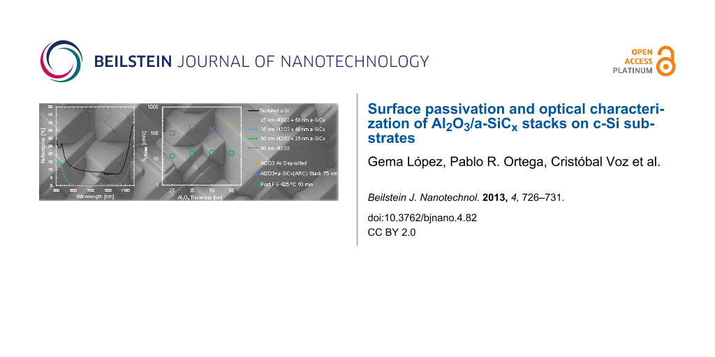
Figure 3: Reflectance curves of Al2O3-coated randomly textured c-Si (a) and polished c-Si (b) for different film thicknesses. Reflectance curves of Al2O3/a-SiCx coated randomly textured c-Si (c) and polished c-Si (d). As a reference, bare polished and textured c-Si reflectances are also included (black line).
Figure 3: Reflectance curves of Al2O3-coated randomly textured c-Si (a) and polished c-Si (b) for different f...
The textured sample without ARC coating (black lines in Figure 3, left) exhibits an integrated average reflectance of 13.3%, much lower than that of polished c-Si substrates. For a randomly textured surface, the reduced reflectance is explained by a second reflection of the incident light at the sidewalls of an opposite pyramid [31]. After coating the silicon substrates, the optical reflectance was further reduced.
When a 90 nm Al2O3 film is deposited on a polished surface, the reflectance yields a minimum of 3.2% at a wavelength of about 600 nm, but it increases quickly for shorter and longer wavelengths. Moreover, the reflectance properties become worse as the Al2O3 film thickness decreases. Next, the reflectance is strongly reduced when the polished samples are coated, but it still increases for longer wavelengths.
On the other hand, when a textured c-Si sample is coated by 90 nm of Al2O3 the reflectance values measured are below 2% between 460 and 1000 nm. Similar results were obtained with the textured samples coated by 75 nm Al2O3/a-SiCx stacks. Thus, both 90 nm Al2O3 film and 75 nm Al2O3/a-SiCx stacks on textured surfaces are excellent anti-reflection options.
Conclusion
Al2O3 layers and Al2O3/a-SiCx stacks with different thicknesses were deposited on polished and randomly textured p- and n-type c-Si substrates by combining thermal ALD and PECVD technique. Outstanding Seff,max values below about 15 cm/s were achieved independently of the surface morphology and doping type of the samples. This value is low enough to obtain highly efficient c-Si solar cells. Concerning the optical properties, the absorbance of Al2O3 layers with different thicknesses and also of different Al2O3/a-SiCx stacks was calculated by evaluating reflectance and transmittance measurements. We found that the absorption loss in a-SiCx layers in the range of short wavelengths of is the reason for the superior overall optical performance of a single 90 nm thick Al2O3 film. Therefore, the latter represents the better option as an antireflection coating compared to Al2O3/a-SiCx stacks. This result is supported by the reflectance measurements of Al2O3 films with different thicknesses and Al2O3/a-SiCx stacks on polished and textured c-Si substrates in the wavelength range from 300 to 1200 nm. In any case, the measured reflectance was less than 2% for all the Al2O3/a-SiCx stacks and also for the single 90 nm layer of Al2O3. Nevertheless, an a-SiCx capping layer could be useful if the Al2O3 layer needs to be protected from some chemical treatment during the solar cell fabrication. Moreover, on the rear side of a c-Si solar cell, where the optical absorbance is not critical, an a-SiCx layer on top of the passivated Al2O3 film acts as a back reflector that reflects photons towards the bulk. This a-SiCx capping layer on the Al2O3 also improves the laser contact formation on p-type c-Si solar cells.
In summary, we can conclude that a 90 nm Al2O3 film on textured c-Si substrates results in a good scheme for both passivation and anti-reflection coating on the illuminated side of highly efficient solar cells, whereas an a-SiCx capping layer on Al2O3 films on the rear side of the solar cell provides better back contacts and a better back reflector scheme.
Experimental
As starting material, n- and p-type (2.5 ± 0.3 Ωcm) FZ silicon(100) wafers with a thickness of approximately 290 µm were used. One p-type and one n-type wafer were textured on both sides with solution of tetramethylammonium hydroxide (TMAH) in isopropanol (IPA) solution. Before film deposition, four wafers, two n-type (one textured and one polished) and two p-type (one textured and one polished) were cleaned following an RCA sequence and cut to quarters. Al2O3 films were subsequently deposited by thermal ALD (Savannah S200, Cambridge Nanotech; Cambridge, MA, USA) at Tdep = 200 °C. This technique is based on sequential, self-limiting chemical reactions at the surface. The surface of the substrate is exposed to the precursor gases in alternating manner. The reactions are cyclical and after each reaction, there is a purge with N2. The typical ALD cycle to deposit Al2O3 layers consists of the injection into the chamber of trimethylaluminum (Al(CH3)3) for 15 ms followed by N2 purging and the injection of water vapour for 50 ms followed by N2 purging. The precursor doses and exposure times were chosen such that all films were deposited under saturated self-limiting conditions leading to a film growth of 1.1 Å/cycle. On each sample, belonging to a different type of wafer, films with a thickness of 25, 35, 50 and 90 nm, respectively, were deposited (deposition times of 38, 53, 73 and 137 min respectively). On top of these films, we deposited an amorphous silicon carbide (a-SiCx) film by PECVD that uses silane (SiH4) and methane (CH4) as precursor gases. The thicknesses of these a-SiCx films were 50, 40 and 25 nm, respectively (deposition times of 12 min 50 sec, 10 min 15 sec and 6 min 24 sec, respectively) in order to complement the 25, 35 and 50 nm Al2O3 films for a total stack thickness of 75 nm. Substrates with an Al2O3 thickness of 90 nm were also studied without any a-SiCx capping layer. A post-deposition annealing process in a forming gas environment (H2/N2) at 425 °C for 10 min was done to activate the passivation properties. All these substrates were symmetrically covered to measure the effective lifetime τeff by measuring the quasi-steady-state photoconductance (QSSPC) with a Wafer Lifetime Tester Sinton WCT-100 [32,33]. The upper limit of the surface recombination velocity (Seff,max) was deduced from the effective lifetime τeff measurements as a function of the excess carrier density (Δn) at 1 sun injection level as
![[2190-4286-4-82-i3]](/bjnano/content/inline/2190-4286-4-82-i3.svg?max-width=590&scale=1.18182)
where W is the substrate thickness and an infinite bulk lifetime has been assumed.
Concerning the optical characterization, the thickness and refractive index of the individual Al2O3 and SiCx layers were measured by ellipsometry (Plasmos SD 2100) at a wavelength of 632 nm. Finally, in order to know the optical absorbance, we also deposited the same Al2O3/a-SiCx stacks on transparent substrates (Borosilicate glass). The reflectance (diffuse and specular) and the transmittance were measured in the wavelength range from 300 to 1200 nm by using a UV–visible–NIR spectrometer (Shimadzu 3600) equipped with an ISR 3100 integrating sphere.
References
-
Hofmann, M.; Janz, S.; Schmidt, C.; Kambor, S.; Suwito, D.; Kohn, N.; Rentsch, J.; Preu, R.; Glunz, S. W. Sol. Energy Mater. Sol. Cells 2009, 93, 1074–1078. doi:10.1016/j.solmat.2008.11.056
Return to citation in text: [1] -
Hoex, B.; Van de Sanden, M. C. M.; Schmidt, J.; Brendel, R.; Kessel, W. M. M. Phys. Status Solidi RRL 2012, 6, 4–6. doi:10.1002/pssr.201105445
Return to citation in text: [1] -
Agostinelli, G.; Delabie, A.; Vitanov, P.; Alexieva, Z.; Dekkers, H. F. W.; De Wolfa, S.; Beaucarne, G. Sol. Energy Mater. Sol. Cells 2006, 90, 3438–3442. doi:10.1016/j.solmat.2006.04.014
Return to citation in text: [1] [2] -
Hoex, B.; Schmidt, J.; Bock, R.; Altermatt, P. P.; van de Sanden, M. C. M.; Kessels, W. M. M. Appl. Phys. Lett. 2007, 91, 112107. doi:10.1063/1.2784168
Return to citation in text: [1] [2] -
Werner, F.; Veith, B.; Tiba, V.; Poodt, P.; Roozeboom, F.; Brendel, R.; Schmidt, J. Appl. Phys. Lett. 2010, 97, 162103. doi:10.1063/1.3505311
Return to citation in text: [1] -
Dingemans, G.; Seguin, R.; Engelhart, P.; van de Sanden, M. C. M.; Kessels, W. M. M. Phys. Status Solidi RRL 2010, 4, 10–12. doi:10.1002/pssr.200903334
Return to citation in text: [1] [2] -
Seguini, G.; Cianci, E.; Wiemer, C.; Saynova, D.; van Rossmalen, J. A. M. Appl. Phys. Lett. 2013, 102, 131603. doi:10.1063/1.4800541
Return to citation in text: [1] [2] -
Liao, B.; Stangl, R.; Mueller, T.; Lin, F.; Bhatia, C. S.; Hoex, B. J. Appl. Phys. 2013, 113, 024509. doi:10.1063/1.4775595
Return to citation in text: [1] -
Hoex, B.; Schmidt, J.; Pohl, P.; van de Sanden, M. C. M.; Kessels, W. M. M. J. Appl. Phys. 2008, 104, 044903. doi:10.1063/1.2963707
Return to citation in text: [1] -
Terlinden, N. M.; Dingemans, G.; van de Sanden, M. C. M.; Kessels, W. M. M. Appl. Phys. Lett. 2010, 96, 112101. doi:10.1063/1.3334729
Return to citation in text: [1] -
Rafí, J. M.; Zabala, M.; Bedarrain, O.; Campabadal, F. J. Electrochem. Soc. 2011, 158, G108–G114. doi:10.1149/1.3559458
Return to citation in text: [1] -
Frascaroli, J.; Seguini, G.; Cianci, E.; Saynova, D.; van Roosmalen, J.; Perego, M. Phys. Status Solidi A 2013, 210, 732–736. doi:10.1002/pssa.201200568
Return to citation in text: [1] -
Lopez, G.; Ortega, P.; Voz, C.; Martín, I.; Colina, M.; Orpella, A.; Alcubilla, R. Optimization of Al2O3 films obtained by ALD to passivate p-type c-Si wafers. In Proccedings of the 27th European Photovoltaic Solar Energy Conference and Exhibition, Frankfurt, Sept 24–28, 2012; Germany, 2012.
Return to citation in text: [1] [2] [3] -
Ortega, P.; Martín, I.; López, G.; Colina, M.; Orpella, A.; Voz, C.; Alcubilla, R. Sol. Energy Mater. Sol. Cells 2012, 106, 80–83. doi:10.1016/j.solmat.2012.05.012
Return to citation in text: [1] -
Martín, I.; Ortega, P.; Colina, M.; Orpella, A.; López, G.; Alcubilla, R. Prog. Photovoltaics 2012, 21, 1171–1175. doi:10.1002/pip.2207
Return to citation in text: [1] -
Green, M. A. Higher Efficiency Silicon Solar cells; Trans. Tech. Pub.: Aedermannsdorf, Switzerland, 1987.
Return to citation in text: [1] -
Dingemans, G.; Terlinden, N. M.; Pierreux, D.; Profijt, H. B.; van de Sanden, M. C. M.; Kessels, W. M. M. Electrochem. Solid-State Lett. 2011, 14, H1–H4. doi:10.1149/1.3501970
Return to citation in text: [1] [2] -
Dingemans, G.; Kessels, W. M. M. J. Vac. Sci. Technol., A 2012, 30, 040802. doi:10.1116/1.4728205
Return to citation in text: [1] [2] [3] [4] -
McIntosh, K. R.; Johnson, L. P. J. Appl. Phys. 2009, 105, 124520. doi:10.1063/1.3153979
Return to citation in text: [1] -
Angermann, H. Appl. Surf. Sci. 2008, 254, 8067–8074. doi:10.1016/j.apsusc.2008.03.022
Return to citation in text: [1] -
Basore, P. A. IEEE Trans. Electron Devices 1990, 37, 337–343. doi:10.1109/16.46362
Return to citation in text: [1] -
Benick, J.; Richter, A.; Hermle, M.; Glunz, S. W. Phys. Status Solidi RRL 2009, 3, 233–235. doi:10.1002/pssr.200903209
Return to citation in text: [1] -
Hoex, B.; Schmidt, J.; Van de Sanden, M. C. M.; Kessels, W. M. M. Crystalline silicon surface passivation by negative-charge-dielectric Al2O3. Photov.Spec.Conf. PVSC 08, 33th IEEE, May 11–16, 2008; pp 1–4.
Return to citation in text: [1] -
Vermang, B.; Goverde, H.; Lorenz, A.; Vereecke, G.; Meersschaut, J.; Corngliotti, E.; Rothschild, A.; John, J.; Poortmans, J.; Mertens, R. On the blistering of atomic layer deposited Al2O3 as Si surface passivation. Photov. Spec. Conf. PVSC11, 37th IEEE, June 19–24, 2011; pp 3562–3567.
Return to citation in text: [1] -
Beldarrain, O.; Duch, M.; Zabala, M.; Rafí, J. M.; Bargalló González, M.; Campabadal, F. J. Vac. Sci. Technol., A 2012, 31, 01A128. doi:10.1116/1.4768170
Return to citation in text: [1] -
Gielis, J. J. H.; Van de Sanden, M. C. M.; Kessels, W. M. M. J. Appl. Phys. 2008, 104, 073701. doi:10.1063/1.3658246
Return to citation in text: [1] -
Dingemans, G.; Terlinden, N. M.; Verheijen, M. A.; van de Sanden, M. C. M.; Kessels, W. M. M. J. Appl. Phys. 2011, 110, 093715. doi:10.1063/1.3658246
Return to citation in text: [1] -
Hoex, B.; Heil, S. B. S.; Langereis, E.; van de Sanden, M. C. M.; Kessels, W. M. M. Appl. Phys. Lett. 2006, 89, 042112. doi:10.1063/1.2240736
Return to citation in text: [1] -
Hoex, B.; Gielis, J. J. H.; van de Sanden, M. C. M.; Kessels, W. M. M. J. Appl. Phys. 2008, 104, 113703. doi:10.1063/1.3021091
Return to citation in text: [1] -
Lei, D.; Yu, X.; Song, L.; Gu, X.; Li, G.; Yang, D. Appl. Phys. Lett. 2011, 99, 052103. doi:10.1063/1.3616145
Return to citation in text: [1] -
Zhao, J.; Green, M. IEEE Trans. Electron Devices 1991, 38, 1925–1934. doi:10.1109/16.119035
Return to citation in text: [1] -
Sinton, R. A.; Cuevas, A. Appl. Phys. Lett. 1996, 69, 2510. doi:10.1063/1.117723
Return to citation in text: [1] -
Cuevas, A.; Macdonald, D. Sol. Energy 2004, 76, 255–262. doi:10.1016/j.solener.2003.07.033
Return to citation in text: [1]
| 18. | Dingemans, G.; Kessels, W. M. M. J. Vac. Sci. Technol., A 2012, 30, 040802. doi:10.1116/1.4728205 |
| 6. | Dingemans, G.; Seguin, R.; Engelhart, P.; van de Sanden, M. C. M.; Kessels, W. M. M. Phys. Status Solidi RRL 2010, 4, 10–12. doi:10.1002/pssr.200903334 |
| 26. | Gielis, J. J. H.; Van de Sanden, M. C. M.; Kessels, W. M. M. J. Appl. Phys. 2008, 104, 073701. doi:10.1063/1.3658246 |
| 27. | Dingemans, G.; Terlinden, N. M.; Verheijen, M. A.; van de Sanden, M. C. M.; Kessels, W. M. M. J. Appl. Phys. 2011, 110, 093715. doi:10.1063/1.3658246 |
| 28. | Hoex, B.; Heil, S. B. S.; Langereis, E.; van de Sanden, M. C. M.; Kessels, W. M. M. Appl. Phys. Lett. 2006, 89, 042112. doi:10.1063/1.2240736 |
| 29. | Hoex, B.; Gielis, J. J. H.; van de Sanden, M. C. M.; Kessels, W. M. M. J. Appl. Phys. 2008, 104, 113703. doi:10.1063/1.3021091 |
| 30. | Lei, D.; Yu, X.; Song, L.; Gu, X.; Li, G.; Yang, D. Appl. Phys. Lett. 2011, 99, 052103. doi:10.1063/1.3616145 |
| 1. | Hofmann, M.; Janz, S.; Schmidt, C.; Kambor, S.; Suwito, D.; Kohn, N.; Rentsch, J.; Preu, R.; Glunz, S. W. Sol. Energy Mater. Sol. Cells 2009, 93, 1074–1078. doi:10.1016/j.solmat.2008.11.056 |
| 11. | Rafí, J. M.; Zabala, M.; Bedarrain, O.; Campabadal, F. J. Electrochem. Soc. 2011, 158, G108–G114. doi:10.1149/1.3559458 |
| 12. | Frascaroli, J.; Seguini, G.; Cianci, E.; Saynova, D.; van Roosmalen, J.; Perego, M. Phys. Status Solidi A 2013, 210, 732–736. doi:10.1002/pssa.201200568 |
| 13. | Lopez, G.; Ortega, P.; Voz, C.; Martín, I.; Colina, M.; Orpella, A.; Alcubilla, R. Optimization of Al2O3 films obtained by ALD to passivate p-type c-Si wafers. In Proccedings of the 27th European Photovoltaic Solar Energy Conference and Exhibition, Frankfurt, Sept 24–28, 2012; Germany, 2012. |
| 9. | Hoex, B.; Schmidt, J.; Pohl, P.; van de Sanden, M. C. M.; Kessels, W. M. M. J. Appl. Phys. 2008, 104, 044903. doi:10.1063/1.2963707 |
| 10. | Terlinden, N. M.; Dingemans, G.; van de Sanden, M. C. M.; Kessels, W. M. M. Appl. Phys. Lett. 2010, 96, 112101. doi:10.1063/1.3334729 |
| 13. | Lopez, G.; Ortega, P.; Voz, C.; Martín, I.; Colina, M.; Orpella, A.; Alcubilla, R. Optimization of Al2O3 films obtained by ALD to passivate p-type c-Si wafers. In Proccedings of the 27th European Photovoltaic Solar Energy Conference and Exhibition, Frankfurt, Sept 24–28, 2012; Germany, 2012. |
| 24. | Vermang, B.; Goverde, H.; Lorenz, A.; Vereecke, G.; Meersschaut, J.; Corngliotti, E.; Rothschild, A.; John, J.; Poortmans, J.; Mertens, R. On the blistering of atomic layer deposited Al2O3 as Si surface passivation. Photov. Spec. Conf. PVSC11, 37th IEEE, June 19–24, 2011; pp 3562–3567. |
| 25. | Beldarrain, O.; Duch, M.; Zabala, M.; Rafí, J. M.; Bargalló González, M.; Campabadal, F. J. Vac. Sci. Technol., A 2012, 31, 01A128. doi:10.1116/1.4768170 |
| 5. | Werner, F.; Veith, B.; Tiba, V.; Poodt, P.; Roozeboom, F.; Brendel, R.; Schmidt, J. Appl. Phys. Lett. 2010, 97, 162103. doi:10.1063/1.3505311 |
| 6. | Dingemans, G.; Seguin, R.; Engelhart, P.; van de Sanden, M. C. M.; Kessels, W. M. M. Phys. Status Solidi RRL 2010, 4, 10–12. doi:10.1002/pssr.200903334 |
| 7. | Seguini, G.; Cianci, E.; Wiemer, C.; Saynova, D.; van Rossmalen, J. A. M. Appl. Phys. Lett. 2013, 102, 131603. doi:10.1063/1.4800541 |
| 8. | Liao, B.; Stangl, R.; Mueller, T.; Lin, F.; Bhatia, C. S.; Hoex, B. J. Appl. Phys. 2013, 113, 024509. doi:10.1063/1.4775595 |
| 17. | Dingemans, G.; Terlinden, N. M.; Pierreux, D.; Profijt, H. B.; van de Sanden, M. C. M.; Kessels, W. M. M. Electrochem. Solid-State Lett. 2011, 14, H1–H4. doi:10.1149/1.3501970 |
| 2. | Hoex, B.; Van de Sanden, M. C. M.; Schmidt, J.; Brendel, R.; Kessel, W. M. M. Phys. Status Solidi RRL 2012, 6, 4–6. doi:10.1002/pssr.201105445 |
| 3. | Agostinelli, G.; Delabie, A.; Vitanov, P.; Alexieva, Z.; Dekkers, H. F. W.; De Wolfa, S.; Beaucarne, G. Sol. Energy Mater. Sol. Cells 2006, 90, 3438–3442. doi:10.1016/j.solmat.2006.04.014 |
| 4. | Hoex, B.; Schmidt, J.; Bock, R.; Altermatt, P. P.; van de Sanden, M. C. M.; Kessels, W. M. M. Appl. Phys. Lett. 2007, 91, 112107. doi:10.1063/1.2784168 |
| 4. | Hoex, B.; Schmidt, J.; Bock, R.; Altermatt, P. P.; van de Sanden, M. C. M.; Kessels, W. M. M. Appl. Phys. Lett. 2007, 91, 112107. doi:10.1063/1.2784168 |
| 23. | Hoex, B.; Schmidt, J.; Van de Sanden, M. C. M.; Kessels, W. M. M. Crystalline silicon surface passivation by negative-charge-dielectric Al2O3. Photov.Spec.Conf. PVSC 08, 33th IEEE, May 11–16, 2008; pp 1–4. |
| 17. | Dingemans, G.; Terlinden, N. M.; Pierreux, D.; Profijt, H. B.; van de Sanden, M. C. M.; Kessels, W. M. M. Electrochem. Solid-State Lett. 2011, 14, H1–H4. doi:10.1149/1.3501970 |
| 18. | Dingemans, G.; Kessels, W. M. M. J. Vac. Sci. Technol., A 2012, 30, 040802. doi:10.1116/1.4728205 |
| 18. | Dingemans, G.; Kessels, W. M. M. J. Vac. Sci. Technol., A 2012, 30, 040802. doi:10.1116/1.4728205 |
| 16. | Green, M. A. Higher Efficiency Silicon Solar cells; Trans. Tech. Pub.: Aedermannsdorf, Switzerland, 1987. |
| 3. | Agostinelli, G.; Delabie, A.; Vitanov, P.; Alexieva, Z.; Dekkers, H. F. W.; De Wolfa, S.; Beaucarne, G. Sol. Energy Mater. Sol. Cells 2006, 90, 3438–3442. doi:10.1016/j.solmat.2006.04.014 |
| 7. | Seguini, G.; Cianci, E.; Wiemer, C.; Saynova, D.; van Rossmalen, J. A. M. Appl. Phys. Lett. 2013, 102, 131603. doi:10.1063/1.4800541 |
| 18. | Dingemans, G.; Kessels, W. M. M. J. Vac. Sci. Technol., A 2012, 30, 040802. doi:10.1116/1.4728205 |
| 22. | Benick, J.; Richter, A.; Hermle, M.; Glunz, S. W. Phys. Status Solidi RRL 2009, 3, 233–235. doi:10.1002/pssr.200903209 |
| 14. | Ortega, P.; Martín, I.; López, G.; Colina, M.; Orpella, A.; Voz, C.; Alcubilla, R. Sol. Energy Mater. Sol. Cells 2012, 106, 80–83. doi:10.1016/j.solmat.2012.05.012 |
| 15. | Martín, I.; Ortega, P.; Colina, M.; Orpella, A.; López, G.; Alcubilla, R. Prog. Photovoltaics 2012, 21, 1171–1175. doi:10.1002/pip.2207 |
| 31. | Zhao, J.; Green, M. IEEE Trans. Electron Devices 1991, 38, 1925–1934. doi:10.1109/16.119035 |
| 13. | Lopez, G.; Ortega, P.; Voz, C.; Martín, I.; Colina, M.; Orpella, A.; Alcubilla, R. Optimization of Al2O3 films obtained by ALD to passivate p-type c-Si wafers. In Proccedings of the 27th European Photovoltaic Solar Energy Conference and Exhibition, Frankfurt, Sept 24–28, 2012; Germany, 2012. |
| 19. | McIntosh, K. R.; Johnson, L. P. J. Appl. Phys. 2009, 105, 124520. doi:10.1063/1.3153979 |
| 20. | Angermann, H. Appl. Surf. Sci. 2008, 254, 8067–8074. doi:10.1016/j.apsusc.2008.03.022 |
| 21. | Basore, P. A. IEEE Trans. Electron Devices 1990, 37, 337–343. doi:10.1109/16.46362 |
| 32. | Sinton, R. A.; Cuevas, A. Appl. Phys. Lett. 1996, 69, 2510. doi:10.1063/1.117723 |
| 33. | Cuevas, A.; Macdonald, D. Sol. Energy 2004, 76, 255–262. doi:10.1016/j.solener.2003.07.033 |
© 2013 López et al; licensee Beilstein-Institut.
This is an Open Access article under the terms of the Creative Commons Attribution License (http://creativecommons.org/licenses/by/2.0), which permits unrestricted use, distribution, and reproduction in any medium, provided the original work is properly cited.
The license is subject to the Beilstein Journal of Nanotechnology terms and conditions: (http://www.beilstein-journals.org/bjnano)