Abstract
We use high-temperature-stable silicon nitride membranes to investigate single layers of silicon nanocrystal ensembles by energy filtered transmission electron microscopy. The silicon nanocrystals are prepared from the precipitation of a silicon-rich oxynitride layer sandwiched between two SiO2 diffusion barriers and subjected to a high-temperature annealing. We find that such single layers are very sensitive to the annealing parameters and may lead to a significant loss of excess silicon. In addition, these ultrathin layers suffer from significant electron beam damage that needs to be minimized in order to image the pristine sample morphology. Finally we demonstrate how the silicon nanocrystal size distribution develops from a broad to a narrow log-normal distribution, when the initial precipitation layer thickness and stoichiometry are below a critical value.
Introduction
Si nanocrystals (Si NC) are interesting for applications in third generation photovoltaics [1,2], light emitting diodes [3,4], lasers [5], but are also envisioned to be used as non-volatile memories [6-10]. The optical and electrical properties of ensembles of Si NCs are strongly influenced by the structural properties such as size distribution, separation distance and density regardless of the application [11-13]. Moreover, there is compelling evidence of multiple exciton generation in adjacent Si NCs with almost ideal quantum efficiencies which is explained in terms of space-separated quantum cutting due to strong coupling between neighboring Si NCs [14-18]. However, clear structural insight on the Si NC size distribution, separation distance and shape is missing to date, largely due to the complexity of the measurement. The distribution of Si NC sizes is routinely obtained by conventional cross-section transmission electron microscopy (TEM) [19,20], but its evaluation is tedious and areal densities and Si NC position and distance to each other cannot be derived with reasonable confidence. Direct attempts have been made to probe size and density of Si NCs by atomic force microscopy [21]. TEM tomography [22,23] and atomprobe tomography [24,25] were also applied, but these methods probe only a very small volume, may be affected by preparation artifacts and require highly sophisticated equipment, enormous computational effort and time. A faster and easier approach to measure the Si NC size, position and density is the use of in-plane energy-filtered TEM (EFTEM) as was demonstrated for Si NCs formed by low energy Si ion implantation [10,26], plasma-enhanced chemical vapor deposition (PE-CVD) [27] or evaporation [28] followed by a high temperature annealing. The bottleneck in such measurements is the low TEM plane view specimen preparation yield when ultrathin layers are concerned. We circumvent this issue in this work by using nanometer thin, free standing silicon nitride membranes to allow for plane view EFTEM analysis without further sample preparation. Thin layers of Si-rich silicon oxynitride (SRON) can be deposited directly on these membranes that also withstand the high temperature annealing that is needed to induce phase separation and crystallization of the Si NC layers. In contrast to the above mentioned ion implantation, deposition processes allow for sharp interfaces between two confining silicon oxide (SiO2) layers. Here, we investigate ultrathin SRON layers by using plane view EFTEM and discuss possible pitfalls in both sample preparation and TEM imaging. Finally, we demonstrate how the thickness and stoichiometry of a SRON layer affects the Si NC size distribution, shape and areal density.
Experimental
We used 5 nm silicon nitride TEM support grids as a substrate (TEMwindows, SN100-A05Q33A). The layers were prepared by PE-CVD the details of which can be found elsewhere [29]. After layer deposition, the samples were postprocessed by high-temperature annealing. A list of all samples including the relevant processing parameters is available in Table 1. The layer stoichiometries were determined by X-ray photoelectron spectroscopy [29,30]. Please note that we sandwiched the SRON layer between two 2 nm SiO2 films to mimic somewhat the SiO2 barrier layer in our superlattice approach [19]. The SiO2 film thickness is a trade-off between contrast quality during the EFTEM investigation and a reduction of the SiO surface loss during annealing [31] that is discussed later on in this paper in more detail. In fact, we do not observe significant Si surface loss when we use 10 nm thick embedding SiO2 layers [32], but the plane view contrast to image Si nanoparticles is strongly reduced due to the largely overlapping plasmon loss peaks of Si and SiO2 centered at 17 eV and 24 eV respectively. Please note that the deposition rates of all sublayers were determined in a separate preliminary experiment by using ellipsometry. The EFTEM has been carried out using an image aberration corrected FEI Titan 80-300 microscope operated at 300 kV, equipped with a Gatan 863 Tridiem Imaging Filter and a US1000 slow-scan CCD camera. EFTEM images were acquired with a 5 eV energy slit centered at an energy loss of 17 eV (i.e., the Si plasmon loss energy).
Table 1: List of TEM membrane samples fabricated within this work.
| sample name | membrane type | active layer | annealing |
|---|---|---|---|
| S1 | 5 nm SiN | 2 nm SiO2/4.5 nm SiO0.64/2 nm SiO2 | 1150 °C, N2, 1 h |
| S2 | 20 nm SiO2 | — | — |
| S3 | 5 nm SiN | 10 nm SiO2 | 1100 °C, N2, 1 h |
| S4 | 5 nm SiN | 2 nm SiO2/10 nm SiO0.93/2 nm SiO2 | 1100 °C, Ara |
| S5 | 5 nm SiN | 2 nm SiO2/10 nm SiO0.93/2 nm SiO2 | 1100 °C, N2a |
| S6 | 5 nm SiN | 2 nm SiO2/4.5 nm SiO0.93/2 nm SiO2 | 1100 °C, N2a |
| S7 | 5 nm SiN | 2 nm SiO2/3.5 nm SiO0.93/2 nm SiO2 | 1100 °C, N2a |
| S8 | 5 nm SiN | 2 nm SiO2/3.5 nm SiO0.85/2 nm SiO2 | 1100 °C, N2a |
| S9 | 5 nm SiN | 2 nm SiO2/3.5 nm SiO0.64/2 nm SiO2 | 1100 °C, N2a |
aannealing was carried in a ramp-up/ramp-down mode with no intentional temperature hold step (see main text for explanation).
Results and Discussion
Electron irradiation damage
First of all, we focus on a more general observation which mainly concerns the thin film instability during the imaging process. In Figure 1a, a TEM micrograph of sample S1 is presented. In the energy-filtered imaging, the Si particles are clearly visible as white areas. The image has been obtained using low-dose conditions with a total dose of about 5.6 C/cm². In Figure 1c, the dose amounts to about 4.5 × 10² C/cm² in the same area. The particles have significantly grown and new particles appeared, which is clearly visualized in the XOR image of Figure 1b, where image changes are indicated by white. We therefore decided to investigate two plain SiO2 films, a SiO2 reference TEM membrane and a SiN membrane with PECVD SiO2 on top (samples S2 and S3, cf. Table 1). As shown in Figure 2, the creation of Si particles also was observed to take place in pure SiO2 and we estimated a threshold irradiation dose of about 16 C/cm². Please note that our calculated threshold dose is in close agreement with literature data [33]. The intense electron beam may cause the breaking of Si–O bonds accompanied by the creation of volatile O2 molecules, which is supported by the observation of defect creation in SiO2 after electron irradiation [34] and a SiO2 thickness dependence on the hole drilling time when exposed to an intense electron probe [35]. Another possible explanation is certainly a preferential sputtering or knock-on of oxygen [36-38]. A common way to reduce the electron beam damage is to lower the operating voltage of the TEM. Hence, we reduced the operation voltage to 80 kV, but did not observe any significant differences in the beam irradiation damage. While the true beam damage mechanism is subject to further investigation, it can be concluded that it is important to take images below the threshold dose, when dielectric films containing Si NCs are investigated.
![[2190-4286-6-99-1]](/bjnano/content/figures/2190-4286-6-99-1.png?scale=2.0&max-width=1024&background=FFFFFF)
Figure 1: EFTEM images of S1: (a) image in fresh area, (c) after about 10 min exposure to an intense electron beam and (b) XOR image of (a) and (c) highlighting the change between the two as denoted by white regions. Nanoparticles obviously grow and even new ones are created.
Figure 1: EFTEM images of S1: (a) image in fresh area, (c) after about 10 min exposure to an intense electron...
![[2190-4286-6-99-2]](/bjnano/content/figures/2190-4286-6-99-2.png?scale=2.0&max-width=1024&background=FFFFFF)
Figure 2: EFTEM images of references samples S2 and S3: (a) S2 irradiated with a low dose, (b) S2 irradiated with a high dose and (c) S3 irradiated with a high dose. After low dose irradiation no Si particles are observed (cf. panel (a)), whereas high doses lead to a dense formation of tiny Si nanoparticles (cf. panels (b) and (c)).
Figure 2: EFTEM images of references samples S2 and S3: (a) S2 irradiated with a low dose, (b) S2 irradiated ...
Silicon loss and out-diffusion during segregation annealing
Another issue that arises directly from inspection of Figure 1a is the low areal density of sample S1 of only 0.8 × 10¹² NC/cm². This is a reduction of more than 50% compared to the value of sample S5 treated with a much lower thermal budget (cf. Table 1 and below in Table 2). Lower Si excess concentrations and smaller SRON thicknesses resulted in even lower areal densities. The results suggest that the single Si NC layer is subject to a loss of excess Si during the annealing process. Oxidation of excess Si by some species in the annealing ambient is unlikely because of the highly purified inert gases used during the annealing process. This is further supported by a control experiment, in which we annealed an oxide free Si wafer under the same annealing conditions. An unintentional oxide growth below 1 nm SiO2 thickness was estimated by ellipsometry. On the other hand, we need to consider Si diffusion towards the surface followed by a molecular desorption process [31]. The diffusion of Si in SiO2 is known to be mediated by co-diffusion of SiO molecules and hence strongly depends on the nature of the Si/SiO2 interface [39]. The diffusion length LSi of Si can be calculated by ![[Graphic 1]](/bjnano/content/inline/2190-4286-6-99-i1.svg?max-width=637&scale=1.18182) , where DSi represents the diffusion constant of Si in SiO2. Using the values from literature [39] for a 1 h annealing, LSi is determined to be around 2.6 nm which is larger than the 2 nm capping SiO2 even though the heating and cooling ramps were not considered. Although the Si surface loss rate is not exactly known, Si out-diffusion and emanation may well explain the observed effects. The diffusion length can be reduced by shortening the annealing time and lowering the annealing temperature. Hence short furnace annealing processes with fast temperature ramps and a peak temperature of 1100 °C are used for all following samples.
, where DSi represents the diffusion constant of Si in SiO2. Using the values from literature [39] for a 1 h annealing, LSi is determined to be around 2.6 nm which is larger than the 2 nm capping SiO2 even though the heating and cooling ramps were not considered. Although the Si surface loss rate is not exactly known, Si out-diffusion and emanation may well explain the observed effects. The diffusion length can be reduced by shortening the annealing time and lowering the annealing temperature. Hence short furnace annealing processes with fast temperature ramps and a peak temperature of 1100 °C are used for all following samples.
The role of annealing ambient
It is well known that N2 annealing is usually reducing interface defects and hence leads to higher photoluminescence intensities as compared to Ar annealing [40,41]. Therefore, 10 nm SiO0.93 films were annealed in Ar and N2 (samples S4 and S5) atmosphere and compared by plane-view EFTEM that is presented in Figure 3. As can be seen at lower magnification (Figure 3a), the Ar-annealed sample exhibits a high density of surface defects. It appears that part of the layer has been removed (darker regions). These surface damages are absent for the N2-annealed sample, which is very homogeneous across the whole sample area. Similar effects have been reported for Ar-annealed SiO2 thin films on Si and were ascribed to out-diffusion of SiO molecules [31]. Therefore, it can be concluded that annealing in N2 hampers the Si out-diffusion. However, the undamaged microstructures (cf. Figure 3b and Figure 3c) are very similar for both annealings. From high resolution TEM (see insets of Figure 3b and Figure 3c) and electron diffraction, we found that both samples feature a high degree of crystallinity as is corrobated by detailed Raman studies [20,42]. However, the Si NC shape is not spherical at all. Due to the minimization of Gibbs free energy, a spherical shape is expected, which is limited by the possibility of atomic rearrangement. Since the phase separation is completed within a few seconds due to diffusion of oxygen [43], the nanoparticle growth and shaping can only be achieved through the diffusion of Si within SiO2, which is extremely low at the used thermal budget. Longer and higher temperature annealings would certainly lead to larger amounts of spherical particles with a reduced density due to late-stage coarsening [27,44].
![[2190-4286-6-99-3]](/bjnano/content/figures/2190-4286-6-99-3.png?scale=2.0&max-width=1024&background=FFFFFF)
Figure 3: EFTEM images of S4 (a,b) and S5 (c): (a) overview image of S4 illustrating severe sample damage caused by Ar annealing, (b,c) smaller area to show that the morphology in the undamaged regions are fairly similar for both Ar and N2 annealing.
Figure 3: EFTEM images of S4 (a,b) and S5 (c): (a) overview image of S4 illustrating severe sample damage cau...
Silicon nanocrystal size distribution and areal density
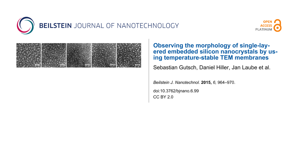
Once the annealing conditions and TEM routines have been specified, it is straightforward to investigate the influence of the SRON layer thickness and stoichiometry on density, size and shape of the Si NCs. In Figure 4 a series of EFTEM images is presented for samples S5 to S9. We first consider Figure 4a–c in which the SRON thickness is reduced from 10 nm to 3.5 nm for a fixed layer stoichiometry of SiO0.93. A transition from irregular and large towards spherical and smaller precipitates is clearly observed. Owing to the excellent contrast, the images can be evaluated by image processing software such as ImageJ [45] in order to analyze the particle distribution. The individual particle areas have been assigned to a circle of the same area which allows for the characterization of all particles through a single parameter. The diameter distributions are shown below the corresponding EFTEM images in Figure 4. All distributions can be fitted excellently by a log-normal distribution. The results strongly reflect the ability to control the Si NC size by geometrical one-dimensional confinement of the SRON layers. Furthermore, the influence of the SRON stoichiometry on Si nanoparticle formation is demonstrated in Figure 4c–e. Interestingly, increasing the Si excess exhibits a similar effect on the Si NC size and shape as the SRON thickness increase. The transition from clustering to spinodal-like decomposition [46-48] is obviously a sensitive function of the SRON thickness as well as of the stoichiometry. Due to the one dimensional geometrical confinement imposed by the SiO2 barriers, the effective excess Si available for particle formation is reduced and hence spinodal growth sets in at higher SRON thicknesses [49]. As the Si excess in the SRON layer is increased, the SRON thickness threshold for spinodal decomposition is shifted to smaller values [49,50], a fact that is experimentally demonstrated in Figure 4.
![[2190-4286-6-99-4]](/bjnano/content/figures/2190-4286-6-99-4.png?scale=2.0&max-width=1024&background=FFFFFF)
Figure 4: EFTEM images and corresponding Si NC size distributions of S5-S9: (a) S5 (10 nm SiO0.93), (b) S6 (4.5 nm SiO0.93), (c) S7 (3.5 nm SiO0.93), (d) S8 (3.5 nm SiO0.85), (e) S9 (3.5 nm SiO0.64).
Figure 4: EFTEM images and corresponding Si NC size distributions of S5-S9: (a) S5 (10 nm SiO0.93), (b) S6 (4...
The EFTEM studies are summarized in Table 2, where the maximum of the diameter distribution as well the particle areal density ANC and the particle area fill fraction are given. Please note that such detailed information as provided by the plane-view method here, is not available in cross-section TEM imaging [19,20,29]. The areal particle density is increased and the Si NC diameter is decreased, when the SRON layer thickness is reduced as expected. However, increasing the Si excess reduces the areal density. The idea of the superlattice approach is to control the Si NC size and density independently by variation of the SRON thickness or stoichiometry respectively [19]. The results presented here are in contrast to the assumptions of this idealized superlattice approach. The reason is apparently that at high Si excess concentrations, larger Si regions form as is indicated by the increased average Si NC diameter. Finally, it must be noted that a certain amount of Si still appears to be lost by Si out-diffusion during the optimized annealing that effectively decreases the particle size.
Table 2: Extracted parameters from the EFTEM analysis, dNC indicates the maximum of the log-normal distribution fit, whereas ANC is the Si NC areal density.
| sample name | SRON layer | dNC (nm) | ANC (NC/cm²) | area fill fraction |
|---|---|---|---|---|
| S5 | 10 nm SiO0.93 | 5.4 | (1.13 ± 0.02) × 1012 | 40.8% |
| S6 | 4.5 nm SiO0.93 | 3.2 | (2.43 ± 0.05) × 1012 | 28.8% |
| S7 | 3.5 nm SiO0.93 | 2.6 | (2.88 ± 0.06) × 1012 | 17.7% |
| S8 | 3.5 nm SiO0.85 | 3.0 | (2.32 ± 0.05) × 1012 | 22.3% |
| S9 | 3.5 nm SiO0.64 | 3.2 | (1.95 ± 0.04) × 1012 | 24.6% |
Conclusion
In conclusion, we have demonstrated an approach using ultrathin TEM membranes and EFTEM imaging as a very versatile tool to study the morphology of Si NC ensembles in contrast to the limitation imposed by cross sectional TEM investigations [19,20,29]. We proved that low electron doses have to be used in order to image the real Si NC structure since higher irradiation doses lead to undesired growth and expansion of the SiNCs. Furthermore, we have shown that for these samples, large surface damage occurs when annealing in Ar atmosphere, whereas this damage is minimized in N2 atmosphere. SiNC size distributions and areal densities were measured for a variety of sample parameters such as initial SRON thickness and stoichiometry. It is demonstrated that SiNC size and density cannot be controlled individually by changing the thickness or stoichiometry of the SRON layer. On the one hand the average SiNC size is controllable by the SRON thickness, on the other hand an increase of the Si excess concentration results in a larger SiNC formation with a reduced areal density. Please note that the observed trends are certainly representative for the given sample parameters, but may still deviate from the individual layer structure in a superlattice.
References
-
Conibeer, G.; Green, M.; Corkish, R.; Cho, Y.; Cho, E.-C.; Jiang, C.-W.; Fangsuwannarak, T.; Pink, E.; Huang, Y.; Puzzer, T.; Trupke, T.; Richards, B.; Shalav, A.; Lin, K.-l. Thin Solid Films 2006, 511–512, 654–662. doi:10.1016/j.tsf.2005.12.119
Return to citation in text: [1] -
Perez-Wurfl, I.; Hao, X.; Gentle, A.; Kim, D.-H.; Conibeer, G.; Green, M. A. Appl. Phys. Lett. 2009, 95, 153506. doi:10.1063/1.3240882
Return to citation in text: [1] -
Marconi, A.; Anopchenko, A.; Wang, M.; Pucker, G.; Bellutti, P.; Pavesi, L. Appl. Phys. Lett. 2009, 94, 221110. doi:10.1063/1.3147164
Return to citation in text: [1] -
Walters, R. J.; Bourianoff, G. I.; Atwater, H. A. Nat. Mater. 2005, 4, 143–146. doi:10.1038/nmat1307
Return to citation in text: [1] -
Pavesi, L.; Dal Negro, L.; Mazzoleni, C.; Franzò, G.; Priolo, F. Nature 2000, 408, 440–444. doi:10.1038/35044012
Return to citation in text: [1] -
Tiwari, S.; Rana, F.; Hanafi, H.; Hartstein, A.; Crabbé, E. F.; Chan, K. Appl. Phys. Lett. 1996, 68, 1377–1379. doi:10.1063/1.116085
Return to citation in text: [1] -
Walters, R. J.; Kik, P. G.; Casperson, J. D.; Atwater, H. A.; Lindstedt, R.; Giorgi, M.; Bourianoff, G. Appl. Phys. Lett. 2004, 85, 2622–2624. doi:10.1063/1.1795364
Return to citation in text: [1] -
Lu, T. Z.; Alexe, M.; Scholz, R.; Talalaev, V.; Zhang, R. J.; Zacharias, M. J. Appl. Phys. 2006, 100, 014310. doi:10.1063/1.2214300
Return to citation in text: [1] -
Lu, T. Z.; Alexe, M.; Scholz, R.; Talelaev, V.; Zacharias, M. Appl. Phys. Lett. 2005, 87, 202110. doi:10.1063/1.2132083
Return to citation in text: [1] -
Müller, T.; Heinig, K.-H.; Möller, W.; Bonafos, C.; Coffin, H.; Cherkashin, N.; Assayag, G. B.; Schamm, S.; Zanchi, G.; Claverie, A.; Tencé, M.; Colliex, C. Appl. Phys. Lett. 2004, 85, 2373–2375. doi:10.1063/1.1794856
Return to citation in text: [1] [2] -
Hartel, A. M.; Gutsch, S.; Hiller, D.; Zacharias, M. Phys. Rev. B 2012, 85, 165306. doi:10.1103/PhysRevB.85.165306
Return to citation in text: [1] -
Gutsch, S.; Laube, J.; Hartel, A. M.; Hiller, D.; Zakharov, N.; Werner, P.; Zacharias, M. J. Appl. Phys. 2013, 113, 133703. doi:10.1063/1.4798395
Return to citation in text: [1] -
López-Vidrier, J.; Berencén, Y.; Hernández, S.; Blázquez, O.; Gutsch, S.; Laube, J.; Hiller, D.; Löper, P.; Schnabel, M.; Janz, S.; Zacharias, M.; Garrido, B. J. Appl. Phys. 2013, 114, 163701. doi:10.1063/1.4826898
Return to citation in text: [1] -
Timmerman, D.; Izeddin, I.; Stallinga, P.; Yassievich, I. N.; Gregorkiewicz, T. Nat. Photonics 2008, 2, 105–109. doi:10.1038/nphoton.2007.279
Return to citation in text: [1] -
Timmerman, D.; Valenta, J.; Dohnalova, K.; de Boer, W. D. A. M.; Gregorkiewicz, T. Nat. Nanotechnol. 2011, 6, 710–713. doi:10.1038/nnano.2011.167
Return to citation in text: [1] -
Trinh, M. T.; Limpens, R.; de Boer, W. D. A. M.; Schins, J. M.; Siebbeles, L. D. A.; Gregorkiewicz, T. Nat. Photonics 2012, 6, 316–321. doi:10.1038/nphoton.2012.36
Return to citation in text: [1] -
Govoni, M.; Marri, I.; Ossicini, S. Nat. Photonics 2012, 6, 672–679. doi:10.1038/nphoton.2012.206
Return to citation in text: [1] -
Valenta, J.; Greben, M.; Gutsch, S.; Hiller, D.; Zacharias, M. Appl. Phys. Lett. 2014, 105, 243107. doi:10.1063/1.4904472
Return to citation in text: [1] -
Zacharias, M.; Heitmann, J.; Scholz, R.; Kahler, U.; Schmidt, M.; Bläsing, J. Appl. Phys. Lett. 2002, 80, 661–663. doi:10.1063/1.1433906
Return to citation in text: [1] [2] [3] [4] [5] -
López-Vidrier, J.; Hernández, S.; Hartel, A. M.; Hiller, D.; Gutsch, S.; Löper, P.; López-Conesa, L.; Estradé, S.; Peiró, F.; Zacharias, M.; Garrido, B. Energy Procedia 2011, 10, 43–48. doi:10.1016/j.egypro.2011.10.150
Return to citation in text: [1] [2] [3] [4] -
Feng, T.; Yu, H.; Dicken, M.; Heath, J. R.; Atwater, H. A. Appl. Phys. Lett. 2005, 86, 033103. doi:10.1063/1.1852078
Return to citation in text: [1] -
Yurtsever, A.; Weyland, M.; Muller, D. A. Appl. Phys. Lett. 2006, 89, 151920. doi:10.1063/1.2360906
Return to citation in text: [1] -
Kourkoutis, L. F.; Hao, X.; Huang, S.; Puthen-Veettil, B.; Conibeer, G.; Green, M. A.; Perez-Wurfl, I. Nanoscale 2013, 5, 7499–7504. doi:10.1039/C3NR01998E
Return to citation in text: [1] -
Talbot, E.; Lardé, R.; Gourbilleau, F.; Dufour, C.; Pareige, P. Europhys. Lett. 2009, 87, 26004. doi:10.1209/0295-5075/87/26004
Return to citation in text: [1] -
Gnaser, H.; Gutsch, S.; Wahl, M.; Schiller, R.; Kopnarski, M.; Hiller, D.; Zacharias, M. J. Appl. Phys. 2014, 115, 034304. doi:10.1063/1.4862174
Return to citation in text: [1] -
Schamm, S.; Bonafos, C.; Coffin, H.; Cherkashin, N.; Carrada, M.; Assayag, G. B.; Claverie, A.; Tencé, M.; Colliex, C. Ultramicroscopy 2008, 108, 346–357. doi:10.1016/j.ultramic.2007.05.008
Return to citation in text: [1] -
Boninelli, S.; Iacona, F.; Franzó, G.; Bongiorno, C.; Spinella, C.; Priolo, F. J. Phys.: Condens. Matter 2007, 19, 225003. doi:10.1088/0953-8984/19/22/225003
Return to citation in text: [1] [2] -
Hernández, S.; Miska, P.; Grün, M.; Estradé, S.; Peiró, F.; Garrido, B.; Vergnat, M.; Pellegrino, P. J. Appl. Phys. 2013, 114, 233101. doi:10.1063/1.4847536
Return to citation in text: [1] -
Hartel, A. M.; Hiller, D.; Gutsch, S.; Löper, P.; Estradé, S.; Peiró, F.; Garrido, B.; Zacharias, M. Thin Solid Films 2011, 520, 121–125. doi:10.1016/j.tsf.2011.06.084
Return to citation in text: [1] [2] [3] [4] -
Laube, J.; Gutsch, S.; Hiller, D.; Bruns, M.; Kübel, C.; Weiss, C.; Zacharias, M. J. Appl. Phys. 2014, 116, 223501. doi:10.1063/1.4904053
Return to citation in text: [1] -
Beyer, V.; von Borany, J.; Heinig, K.-H. J. Appl. Phys. 2007, 101, 053516. doi:10.1063/1.2436834
Return to citation in text: [1] [2] [3] -
Hartel, A. M.; Gutsch, S.; Hiller, D.; Kübel, C.; Zakharov, N.; Werner, P.; Zacharias, M. Appl. Phys. Lett. 2012, 101, 193103. doi:10.1063/1.4766284
Return to citation in text: [1] -
Chen, G. S.; Boothroyd, C. B.; Humphreys, C. J. Philos. Mag. A 1998, 78, 491–506. doi:10.1080/01418619808241915
Return to citation in text: [1] -
Pfeffer, R. L. J. Appl. Phys. 1985, 57, 5176–5180. doi:10.1063/1.335252
Return to citation in text: [1] -
Chen, G. S.; Humphreys, C. J. J. Appl. Phys. 1999, 85, 148–152. doi:10.1063/1.369461
Return to citation in text: [1] -
Egerton, R. F.; Li, P.; Malac, M. Micron 2004, 35, 399–409. doi:10.1016/j.micron.2004.02.003
Return to citation in text: [1] -
Egerton, R. F.; McLeod, R.; Wang, F.; Malac, M. Ultramicroscopy 2010, 110, 991–997. doi:10.1016/j.ultramic.2009.11.003
Return to citation in text: [1] -
Egerton, R. F.; Wang, F.; Crozier, P. A. Microsc. Microanal. 2006, 12, 65–71. doi:10.1017/S1431927606060065
Return to citation in text: [1] -
Uematsu, M.; Kageshima, H.; Takahashi, Y.; Fukatsu, S.; Itoh, K. M.; Shiraishi, K.; Gösele, U. Appl. Phys. Lett. 2004, 84, 876–878. doi:10.1063/1.1644623
Return to citation in text: [1] [2] -
Hiller, D.; Goetze, S.; Munnik, F.; Jivanescu, M.; Gerlach, J. W.; Vogt, J.; Pippel, E.; Zakharov, N.; Stesmans, A.; Zacharias, M. Phys. Rev. B 2010, 82, 195401. doi:10.1103/PhysRevB.82.195401
Return to citation in text: [1] -
Wilkinson, A. R.; Elliman, R. G. J. Appl. Phys. 2004, 96, 4018–4020. doi:10.1063/1.1789265
Return to citation in text: [1] -
Hernández, S.; López-Vidrier, J.; López-Conesa, L.; Hiller, D.; Gutsch, S.; Ibáñez, J.; Estradé, S.; Peiró, F.; Zacharias, M.; Garrido, B. J. Appl. Phys. 2014, 115, 203504. doi:10.1063/1.4878175
Return to citation in text: [1] -
Sarikov, A.; Litovchenko, V.; Lisovskyy, I.; Maidanchuk, I.; Zlobin, S. Appl. Phys. Lett. 2007, 91, 133109. doi:10.1063/1.2790814
Return to citation in text: [1] -
Rogers, T. M.; Desai, R. C. Phys. Rev. B 1989, 39, 11956–11964. doi:10.1103/PhysRevB.39.11956
Return to citation in text: [1] -
ImageJ. http://imagej.nih.gov/ij/ (accessed March 9, 2015).
Return to citation in text: [1] -
Cahn, J. W. J. Chem. Phys. 1965, 42, 93–99. doi:10.1063/1.1695731
Return to citation in text: [1] -
Abyzov, A. S.; Schmelzer, J. W. P. J. Chem. Phys. 2007, 127, 114504. doi:10.1063/1.2774989
Return to citation in text: [1] -
Brunini, V. E.; Schuh, C. A.; Carter, W. C. Phys. Rev. E 2011, 83, 021119. doi:10.1103/PhysRevE.83.021119
Return to citation in text: [1] -
Binder, K.; Puri, S.; Das, S. K.; Horbach, J. J. Stat. Phys. 2010, 138, 51–84. doi:10.1007/s10955-010-9924-9
Return to citation in text: [1] [2] -
Müller, T.; Heinig, K.-H.; Möller, W. Appl. Phys. Lett. 2002, 81, 3049–3051. doi:10.1063/1.1512952
Return to citation in text: [1]
| 20. | López-Vidrier, J.; Hernández, S.; Hartel, A. M.; Hiller, D.; Gutsch, S.; Löper, P.; López-Conesa, L.; Estradé, S.; Peiró, F.; Zacharias, M.; Garrido, B. Energy Procedia 2011, 10, 43–48. doi:10.1016/j.egypro.2011.10.150 |
| 42. | Hernández, S.; López-Vidrier, J.; López-Conesa, L.; Hiller, D.; Gutsch, S.; Ibáñez, J.; Estradé, S.; Peiró, F.; Zacharias, M.; Garrido, B. J. Appl. Phys. 2014, 115, 203504. doi:10.1063/1.4878175 |
| 43. | Sarikov, A.; Litovchenko, V.; Lisovskyy, I.; Maidanchuk, I.; Zlobin, S. Appl. Phys. Lett. 2007, 91, 133109. doi:10.1063/1.2790814 |
| 27. | Boninelli, S.; Iacona, F.; Franzó, G.; Bongiorno, C.; Spinella, C.; Priolo, F. J. Phys.: Condens. Matter 2007, 19, 225003. doi:10.1088/0953-8984/19/22/225003 |
| 44. | Rogers, T. M.; Desai, R. C. Phys. Rev. B 1989, 39, 11956–11964. doi:10.1103/PhysRevB.39.11956 |
| 1. | Conibeer, G.; Green, M.; Corkish, R.; Cho, Y.; Cho, E.-C.; Jiang, C.-W.; Fangsuwannarak, T.; Pink, E.; Huang, Y.; Puzzer, T.; Trupke, T.; Richards, B.; Shalav, A.; Lin, K.-l. Thin Solid Films 2006, 511–512, 654–662. doi:10.1016/j.tsf.2005.12.119 |
| 2. | Perez-Wurfl, I.; Hao, X.; Gentle, A.; Kim, D.-H.; Conibeer, G.; Green, M. A. Appl. Phys. Lett. 2009, 95, 153506. doi:10.1063/1.3240882 |
| 11. | Hartel, A. M.; Gutsch, S.; Hiller, D.; Zacharias, M. Phys. Rev. B 2012, 85, 165306. doi:10.1103/PhysRevB.85.165306 |
| 12. | Gutsch, S.; Laube, J.; Hartel, A. M.; Hiller, D.; Zakharov, N.; Werner, P.; Zacharias, M. J. Appl. Phys. 2013, 113, 133703. doi:10.1063/1.4798395 |
| 13. | López-Vidrier, J.; Berencén, Y.; Hernández, S.; Blázquez, O.; Gutsch, S.; Laube, J.; Hiller, D.; Löper, P.; Schnabel, M.; Janz, S.; Zacharias, M.; Garrido, B. J. Appl. Phys. 2013, 114, 163701. doi:10.1063/1.4826898 |
| 29. | Hartel, A. M.; Hiller, D.; Gutsch, S.; Löper, P.; Estradé, S.; Peiró, F.; Garrido, B.; Zacharias, M. Thin Solid Films 2011, 520, 121–125. doi:10.1016/j.tsf.2011.06.084 |
| 30. | Laube, J.; Gutsch, S.; Hiller, D.; Bruns, M.; Kübel, C.; Weiss, C.; Zacharias, M. J. Appl. Phys. 2014, 116, 223501. doi:10.1063/1.4904053 |
| 19. | Zacharias, M.; Heitmann, J.; Scholz, R.; Kahler, U.; Schmidt, M.; Bläsing, J. Appl. Phys. Lett. 2002, 80, 661–663. doi:10.1063/1.1433906 |
| 20. | López-Vidrier, J.; Hernández, S.; Hartel, A. M.; Hiller, D.; Gutsch, S.; Löper, P.; López-Conesa, L.; Estradé, S.; Peiró, F.; Zacharias, M.; Garrido, B. Energy Procedia 2011, 10, 43–48. doi:10.1016/j.egypro.2011.10.150 |
| 29. | Hartel, A. M.; Hiller, D.; Gutsch, S.; Löper, P.; Estradé, S.; Peiró, F.; Garrido, B.; Zacharias, M. Thin Solid Films 2011, 520, 121–125. doi:10.1016/j.tsf.2011.06.084 |
| 6. | Tiwari, S.; Rana, F.; Hanafi, H.; Hartstein, A.; Crabbé, E. F.; Chan, K. Appl. Phys. Lett. 1996, 68, 1377–1379. doi:10.1063/1.116085 |
| 7. | Walters, R. J.; Kik, P. G.; Casperson, J. D.; Atwater, H. A.; Lindstedt, R.; Giorgi, M.; Bourianoff, G. Appl. Phys. Lett. 2004, 85, 2622–2624. doi:10.1063/1.1795364 |
| 8. | Lu, T. Z.; Alexe, M.; Scholz, R.; Talalaev, V.; Zhang, R. J.; Zacharias, M. J. Appl. Phys. 2006, 100, 014310. doi:10.1063/1.2214300 |
| 9. | Lu, T. Z.; Alexe, M.; Scholz, R.; Talelaev, V.; Zacharias, M. Appl. Phys. Lett. 2005, 87, 202110. doi:10.1063/1.2132083 |
| 10. | Müller, T.; Heinig, K.-H.; Möller, W.; Bonafos, C.; Coffin, H.; Cherkashin, N.; Assayag, G. B.; Schamm, S.; Zanchi, G.; Claverie, A.; Tencé, M.; Colliex, C. Appl. Phys. Lett. 2004, 85, 2373–2375. doi:10.1063/1.1794856 |
| 19. | Zacharias, M.; Heitmann, J.; Scholz, R.; Kahler, U.; Schmidt, M.; Bläsing, J. Appl. Phys. Lett. 2002, 80, 661–663. doi:10.1063/1.1433906 |
| 5. | Pavesi, L.; Dal Negro, L.; Mazzoleni, C.; Franzò, G.; Priolo, F. Nature 2000, 408, 440–444. doi:10.1038/35044012 |
| 28. | Hernández, S.; Miska, P.; Grün, M.; Estradé, S.; Peiró, F.; Garrido, B.; Vergnat, M.; Pellegrino, P. J. Appl. Phys. 2013, 114, 233101. doi:10.1063/1.4847536 |
| 19. | Zacharias, M.; Heitmann, J.; Scholz, R.; Kahler, U.; Schmidt, M.; Bläsing, J. Appl. Phys. Lett. 2002, 80, 661–663. doi:10.1063/1.1433906 |
| 20. | López-Vidrier, J.; Hernández, S.; Hartel, A. M.; Hiller, D.; Gutsch, S.; Löper, P.; López-Conesa, L.; Estradé, S.; Peiró, F.; Zacharias, M.; Garrido, B. Energy Procedia 2011, 10, 43–48. doi:10.1016/j.egypro.2011.10.150 |
| 29. | Hartel, A. M.; Hiller, D.; Gutsch, S.; Löper, P.; Estradé, S.; Peiró, F.; Garrido, B.; Zacharias, M. Thin Solid Films 2011, 520, 121–125. doi:10.1016/j.tsf.2011.06.084 |
| 3. | Marconi, A.; Anopchenko, A.; Wang, M.; Pucker, G.; Bellutti, P.; Pavesi, L. Appl. Phys. Lett. 2009, 94, 221110. doi:10.1063/1.3147164 |
| 4. | Walters, R. J.; Bourianoff, G. I.; Atwater, H. A. Nat. Mater. 2005, 4, 143–146. doi:10.1038/nmat1307 |
| 29. | Hartel, A. M.; Hiller, D.; Gutsch, S.; Löper, P.; Estradé, S.; Peiró, F.; Garrido, B.; Zacharias, M. Thin Solid Films 2011, 520, 121–125. doi:10.1016/j.tsf.2011.06.084 |
| 19. | Zacharias, M.; Heitmann, J.; Scholz, R.; Kahler, U.; Schmidt, M.; Bläsing, J. Appl. Phys. Lett. 2002, 80, 661–663. doi:10.1063/1.1433906 |
| 22. | Yurtsever, A.; Weyland, M.; Muller, D. A. Appl. Phys. Lett. 2006, 89, 151920. doi:10.1063/1.2360906 |
| 23. | Kourkoutis, L. F.; Hao, X.; Huang, S.; Puthen-Veettil, B.; Conibeer, G.; Green, M. A.; Perez-Wurfl, I. Nanoscale 2013, 5, 7499–7504. doi:10.1039/C3NR01998E |
| 10. | Müller, T.; Heinig, K.-H.; Möller, W.; Bonafos, C.; Coffin, H.; Cherkashin, N.; Assayag, G. B.; Schamm, S.; Zanchi, G.; Claverie, A.; Tencé, M.; Colliex, C. Appl. Phys. Lett. 2004, 85, 2373–2375. doi:10.1063/1.1794856 |
| 26. | Schamm, S.; Bonafos, C.; Coffin, H.; Cherkashin, N.; Carrada, M.; Assayag, G. B.; Claverie, A.; Tencé, M.; Colliex, C. Ultramicroscopy 2008, 108, 346–357. doi:10.1016/j.ultramic.2007.05.008 |
| 49. | Binder, K.; Puri, S.; Das, S. K.; Horbach, J. J. Stat. Phys. 2010, 138, 51–84. doi:10.1007/s10955-010-9924-9 |
| 21. | Feng, T.; Yu, H.; Dicken, M.; Heath, J. R.; Atwater, H. A. Appl. Phys. Lett. 2005, 86, 033103. doi:10.1063/1.1852078 |
| 27. | Boninelli, S.; Iacona, F.; Franzó, G.; Bongiorno, C.; Spinella, C.; Priolo, F. J. Phys.: Condens. Matter 2007, 19, 225003. doi:10.1088/0953-8984/19/22/225003 |
| 49. | Binder, K.; Puri, S.; Das, S. K.; Horbach, J. J. Stat. Phys. 2010, 138, 51–84. doi:10.1007/s10955-010-9924-9 |
| 50. | Müller, T.; Heinig, K.-H.; Möller, W. Appl. Phys. Lett. 2002, 81, 3049–3051. doi:10.1063/1.1512952 |
| 19. | Zacharias, M.; Heitmann, J.; Scholz, R.; Kahler, U.; Schmidt, M.; Bläsing, J. Appl. Phys. Lett. 2002, 80, 661–663. doi:10.1063/1.1433906 |
| 20. | López-Vidrier, J.; Hernández, S.; Hartel, A. M.; Hiller, D.; Gutsch, S.; Löper, P.; López-Conesa, L.; Estradé, S.; Peiró, F.; Zacharias, M.; Garrido, B. Energy Procedia 2011, 10, 43–48. doi:10.1016/j.egypro.2011.10.150 |
| 14. | Timmerman, D.; Izeddin, I.; Stallinga, P.; Yassievich, I. N.; Gregorkiewicz, T. Nat. Photonics 2008, 2, 105–109. doi:10.1038/nphoton.2007.279 |
| 15. | Timmerman, D.; Valenta, J.; Dohnalova, K.; de Boer, W. D. A. M.; Gregorkiewicz, T. Nat. Nanotechnol. 2011, 6, 710–713. doi:10.1038/nnano.2011.167 |
| 16. | Trinh, M. T.; Limpens, R.; de Boer, W. D. A. M.; Schins, J. M.; Siebbeles, L. D. A.; Gregorkiewicz, T. Nat. Photonics 2012, 6, 316–321. doi:10.1038/nphoton.2012.36 |
| 17. | Govoni, M.; Marri, I.; Ossicini, S. Nat. Photonics 2012, 6, 672–679. doi:10.1038/nphoton.2012.206 |
| 18. | Valenta, J.; Greben, M.; Gutsch, S.; Hiller, D.; Zacharias, M. Appl. Phys. Lett. 2014, 105, 243107. doi:10.1063/1.4904472 |
| 24. | Talbot, E.; Lardé, R.; Gourbilleau, F.; Dufour, C.; Pareige, P. Europhys. Lett. 2009, 87, 26004. doi:10.1209/0295-5075/87/26004 |
| 25. | Gnaser, H.; Gutsch, S.; Wahl, M.; Schiller, R.; Kopnarski, M.; Hiller, D.; Zacharias, M. J. Appl. Phys. 2014, 115, 034304. doi:10.1063/1.4862174 |
| 46. | Cahn, J. W. J. Chem. Phys. 1965, 42, 93–99. doi:10.1063/1.1695731 |
| 47. | Abyzov, A. S.; Schmelzer, J. W. P. J. Chem. Phys. 2007, 127, 114504. doi:10.1063/1.2774989 |
| 48. | Brunini, V. E.; Schuh, C. A.; Carter, W. C. Phys. Rev. E 2011, 83, 021119. doi:10.1103/PhysRevE.83.021119 |
| 33. | Chen, G. S.; Boothroyd, C. B.; Humphreys, C. J. Philos. Mag. A 1998, 78, 491–506. doi:10.1080/01418619808241915 |
| 31. | Beyer, V.; von Borany, J.; Heinig, K.-H. J. Appl. Phys. 2007, 101, 053516. doi:10.1063/1.2436834 |
| 32. | Hartel, A. M.; Gutsch, S.; Hiller, D.; Kübel, C.; Zakharov, N.; Werner, P.; Zacharias, M. Appl. Phys. Lett. 2012, 101, 193103. doi:10.1063/1.4766284 |
| 40. | Hiller, D.; Goetze, S.; Munnik, F.; Jivanescu, M.; Gerlach, J. W.; Vogt, J.; Pippel, E.; Zakharov, N.; Stesmans, A.; Zacharias, M. Phys. Rev. B 2010, 82, 195401. doi:10.1103/PhysRevB.82.195401 |
| 41. | Wilkinson, A. R.; Elliman, R. G. J. Appl. Phys. 2004, 96, 4018–4020. doi:10.1063/1.1789265 |
| 31. | Beyer, V.; von Borany, J.; Heinig, K.-H. J. Appl. Phys. 2007, 101, 053516. doi:10.1063/1.2436834 |
| 39. | Uematsu, M.; Kageshima, H.; Takahashi, Y.; Fukatsu, S.; Itoh, K. M.; Shiraishi, K.; Gösele, U. Appl. Phys. Lett. 2004, 84, 876–878. doi:10.1063/1.1644623 |
| 39. | Uematsu, M.; Kageshima, H.; Takahashi, Y.; Fukatsu, S.; Itoh, K. M.; Shiraishi, K.; Gösele, U. Appl. Phys. Lett. 2004, 84, 876–878. doi:10.1063/1.1644623 |
| 36. | Egerton, R. F.; Li, P.; Malac, M. Micron 2004, 35, 399–409. doi:10.1016/j.micron.2004.02.003 |
| 37. | Egerton, R. F.; McLeod, R.; Wang, F.; Malac, M. Ultramicroscopy 2010, 110, 991–997. doi:10.1016/j.ultramic.2009.11.003 |
| 38. | Egerton, R. F.; Wang, F.; Crozier, P. A. Microsc. Microanal. 2006, 12, 65–71. doi:10.1017/S1431927606060065 |
| 31. | Beyer, V.; von Borany, J.; Heinig, K.-H. J. Appl. Phys. 2007, 101, 053516. doi:10.1063/1.2436834 |
| 35. | Chen, G. S.; Humphreys, C. J. J. Appl. Phys. 1999, 85, 148–152. doi:10.1063/1.369461 |
© 2015 Gutsch et al; licensee Beilstein-Institut.
This is an Open Access article under the terms of the Creative Commons Attribution License (http://creativecommons.org/licenses/by/2.0), which permits unrestricted use, distribution, and reproduction in any medium, provided the original work is properly cited.
The license is subject to the Beilstein Journal of Nanotechnology terms and conditions: (http://www.beilstein-journals.org/bjnano)