Abstract
The nanoscale morphology of photoactive hybrid heterojunctions plays a key role in the performances of hybrid solar cells. In this work, the heterojunctions consist of a nanocolumnar TiO2 surface covalently grafted with a monolayer of poly(3-hexylthiophene) (P3HT) functionalized with carboxylic groups (–COOH). Through a joint analysis of the photovoltaic properties at the nanoscale by photoconductive-AFM (PC-AFM) and surface photovoltage imaging, we investigated the physical mechanisms taking place locally during the photovoltaic process and the correlation to the nanoscale morphology. A down-shift of the vacuum level of the TiO2 surface upon grafting was measured by Kelvin probe force microscopy (KPFM), evidencing the formation of a dipole at the TiO2/P3HT-COOH interface. Upon in situ illumination, a positive photovoltage was observed as a result of the accumulation of photogenerated holes in the P3HT layer. A positive photocurrent was recorded in PC-AFM measurements, whose spatial mapping was interpreted consistently with the corresponding KPFM analysis, offering a correlated analysis of interest from both a theoretical and material design perspective.
Introduction
Over the past decades, a large range of photovoltaic (PV) technologies have been developed for the production of renewable energy [1]. Inorganic photovoltaic cells are currently the most employed PV devices with a power efficiency ranging from 20 to 40% [2] and a long-term stability up to 20 years [3]. However, a number of drawbacks affect those technologies. Indeed, in addition to high energy consumption for their fabrication, these devices are deposited on rigid substrates and involve relatively heavy and costly materials of possibly low abundance and/or toxicity [4]. New PV technologies, such as organic photovoltaics (OPV) and hybrid solar cells, are now being developed [2] to cope with such issues. In particular, hybrid solar cells can possibly benefit from the low economic and energy costs of production, high absorbance and tailorable absorption spectrum of the organic materials on the one hand, and from the good stability, absorption and electrical properties of the inorganic materials on the other hand.
Hybrid PV devices include various technologies such as perovskite cells, dye sensitized solar cells (DSSC), with power efficiencies up to 13% [5] and hybrid bulk heterojunctions (HBHJ), which combine an organic matrix and inorganic semiconducting nanostructures such as quantum dots. Among the electron acceptor materials commonly used for DSSC and HBHJ, titanium dioxide (TiO2) is a well-known metal oxide semiconductor [6-8]. Depending on its nanostructure and its crystalline phase, its conductivity varies from 10−4 Ω−1·cm−1 to 10−11 Ω−1·cm−1 [9,10]. TiO2 is very valuable because it can easily form nanostructures, such as nanoporous layers, nanowires or nanocolumns [5,11,12]. Because of its large band gap (3.2 eV [13]), light absorption is carried out by an organic or inorganic dye. The nanostructuration of the acceptor material is crucial for the cell performance [11], as it allows increasing the specific surface of the layer to enhance the amount of grafted dye, and thereby, the photon absorption yield. Nanostructuration is also likely to improve the conductivity of TiO2 [14]. Because of the influence of the nanostructuration of TiO2 on the optoelectronic properties of the device, it is of prime interest to study the photovoltaic properties at the nanoscale. Hybrid heterojunction (HHJ) structures are obtained by impregnation of the porous layer with an absorbing dye or a polymer electron donor. Poly(3-hexylthiophene) (P3HT) is often used, because of its strong absorption, its high hole mobility and its donor-like electronic properties [15]. Upon light absorption by the polymer, excitons are generated and they can be dissociated at the interface with TiO2, the polymer also acting as the hole-transporting layer.
In this work, we investigated nanostructured TiO2 layers composed of arrays of nanoscale columns, covalently sensitized with a P3HT-COOH monolayer to form hybrid bulk heterojunctions. The grafting of P3HT on the surface of TiO2, ensured by the COOH groups, was demonstrated to be beneficial for the photoconversion efficiency of the system [16-18]. The vertically aligned nanostructuration of TiO2 also makes this system attractive, since it ensures direct percolation paths for the photogenerated electrons from the donor–acceptor interface to the cathode, while providing a simple, controlled and ordered architecture. Furthermore, studies are available in literature regarding the photovoltaic response of TiO2/P3HT blends [16-23] and can be used as a reference for meaningful interpretations of our measurements, both in terms of photocurrent and photovoltage under illumination. The columnar TiO2/P3HT-COOH HHJs have been studied by photoconductive-AFM (PC-AFM) and photo-assisted Kelvin probe force microscopy (photo-KPFM) to follow the photovoltaic response, i.e., photocurrent and photovoltage, respectively, at the nanoscale under illumination, in order to understand the local physical processes taking place during the photoconversion of energy, and their correlation with the nanoscale morphology of the active layer. A key aspect of this work consists in the joint analysis of these correlated PC-AFM and KPFM measurements, providing a more fundamental understanding of the photovoltaic mechanisms at stake in the systems. To the best of our knowledge, this joint KPFM/PC-AFM study of such a nanostructured array of TiO2 columns sensitized with functionalized P3HT-COOH constitutes a novel result of interest from both a theoretical and material design perspectives.
Materials and Methods
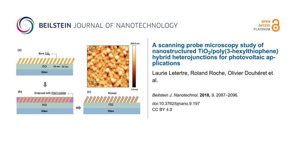
The TiO2 layers were synthesized by magnetron sputtering in grazing mode. A thorough description of the fabrication process can be found in the literature [24], which also identified the optimized fabrication parameters for prospective photovoltaic applications. In compliance with these recommendations, the layers were synthesized without any substrate rotation or bias, while fixing the growth temperature to 450 °C and the tilt angle between the substrate and the cathode axis to 60°. Anatase TiO2 layers with a 200 nm thick nanocolumnar morphology have been deposited on 85 nm-thick ITO-coated glass substrates (Naranjo B.V., sheet resistance of 15 Ω·sq). The average spacing between the columns is (10 ± 3) nm, with an average width of the columns of (19 ± 4) nm, as determined by SEM measurements [24]. The topography of the deposit is shown in the tapping-mode atomic force microscopy (TM-AFM) image of Figure 1d, where the apex of the columns appears as hemispherical protuberances. Regio-regular P3HT-COOH (5400 g/mol, which corresponds to about 30 monomer units, i.e., a total polymer chain length around 130 Å) was synthesized following a reported procedure [24]. A schematic description of the grafting protocol is given in Figure 1a–c. The polymer deposit was obtained by dropcasting a 0.5 mg/mL solution of P3HT-COOH in chlorobenzene on the TiO2 structure. The covalent grafting of the polymer on the nanoporous TiO2 surface is ensured by the carboxylic –COOH group. Rinsing with chlorobenzene was then carried out to remove the residual ungrafted polymer chains. The success of the polymer grafting is confirmed by UV–visible optical absorption measurement across a 350–800 nm wavelength range, for which an absorption of light higher by one order of magnitude compared to bare TiO2 was measured [24]. This indicates a good P3HT impregnation along the columns, the interspacing being sufficient for the polymer infiltration.
![[2190-4286-9-197-1]](/bjnano/content/figures/2190-4286-9-197-1.png?scale=2.0&max-width=1024&background=FFFFFF)
Figure 1: (a–c) Schematic representation of the TiO2/P3HT-COOH HHJ preparation. (d) 2 × 2 µm2 TM-AFM height image of a bare nanocolumnar TiO2 layer.
Figure 1: (a–c) Schematic representation of the TiO2/P3HT-COOH HHJ preparation. (d) 2 × 2 µm2 TM-AFM height i...
The photo-KPFM measurements were carried out in a UHV (<10−10 Torr) instrument composed of an Omicron Nanotechnology VT-AFM system with a Nanonis controller. The KPFM electrical excitation used a frequency ωKPFM/2π of 958 Hz, with a VAC amplitude of 600 mV. The light source for sample irradiation was a green laser diode (wavelength = 500 nm, power density = 1.45 mW/mm2). Photo-assisted KPFM measurements were also performed in ambient conditions, with a Bruker multimode microscope controlled by a Nanoscope III unit coupled to a Nanonis control unit (SPECS Zürich). The KPFM electrical excitation was made at a frequency ωKPFM/2π of 80 Hz, with a VAC amplitude of 500 mV. The illumination of the sample for photo-KPFM and photovoltage probing was provided by a white light lamp irradiating the sample surface from the top. In both setups, conductive Nanosensors PPP-EFM tips (PtIr-coated Si probes) were used (resonant frequency around 75 kHz). The sample was grounded while the excitation and regulation biases were applied to the tip. The measured contact potential difference (Vcpd) is given by the following expression:
![[2190-4286-9-197-i1]](/bjnano/content/inline/2190-4286-9-197-i1.svg?max-width=590&scale=1.18182)
where Φtip and Φsample are the workfunction of the tip and the sample, respectively. In this work, no calibration of the tip workfunction was necessary, as only the Vcpd variations between the materials constituting the photovoltaic blends and their modifications with incoming light were to be measured. These Vcpd variations provide relative but quantitative variations of surface potential at the investigated interfaces.
The PC-AFM measurements were carried out in air, using a Bruker Dimension Icon microscope with a Nanoscope V controller. An extended TUNA external module was used for current detection with a detection range within 100 fA to 1 µA. Silicon tips coated with a PtIr conductive alloy (PPP-CONTPt from Nanosensors) were used. The tip and the back-contact were connected while the sample was locally irradiated from the bottom (through the patterned ITO–glass substrates) under AM 1.5 calibrated white light illumination (spot diameter around 200 µm, power density of 100 suns).
Results and Discussion
Photo-KPFM measurements on the TiO2/P3HT-COOH hybrid heterojunctions
Analysis of the Vcpd contrast in the dark
Figure 2a shows a 500 × 500 nm2 AFM height image obtained in UHV on a nanocolumnar TiO2 film deposited over a grounded ITO electrode, where the nanocolumns of TiO2 are assembled in clumps with a width of several hundred nm. Figure 2b shows the corresponding KPFM Vcpd image. Figure 2c presents the three-dimensional display of Figure 2a, where the colour scale refers to the Vcpd signal of Figure 2b. The distribution of the Vcpd values can be fit with a Gaussian distribution centred at −931 mV with a FWHM of 97 mV (Figure 2d).
![[2190-4286-9-197-2]](/bjnano/content/figures/2190-4286-9-197-2.png?scale=2.0&max-width=1024&background=FFFFFF)
Figure 2: (a) 500 × 500 nm2 AFM height image of a nanostructured TiO2 film, obtained in UHV. Height detection parameters: −22 Hz of frequency shift setpoint and 40 mV of amplitude setpoint. (b) Corresponding KPFM Vcpd image. Vcpd detection parameters: frequency and amplitude of the electrical excitation: 958 Hz and 600 mV. (c) Three-dimensional display of the height image (a), shown with the color scale of the Vcpd (b). (d) Vcpd histogram extracted from (b) (black line) superimposed with a Gaussian fit (red curve).
Figure 2: (a) 500 × 500 nm2 AFM height image of a nanostructured TiO2 film, obtained in UHV. Height detection...
A direct correlation between the topography and the Vcpd signal can be observed, with a higher height corresponding to a more negative Vcpd. It is however unlikely that the contrast purely originates from a crosstalk between the topography and the Vcpd, as indicated by local mismatching between both contrasts (see red lines in Figure 2a and 2b). Moreover, further measurements (see Figure 3) showed that P3HT grafting barely affects the overall morphology but smooths tremendously the Vcpd contrast. Thus, the observed Vcpd contrast most probably originates therefore from local variations in the electronic properties of the surface, such as a possibly different free electron density at the top and at the side of the columns. This explanation is further supported by the PC-AFM measurements presented in the last section. As shown in the Supporting Information File 1 (Figure S1), no ungrounded potential is to be detected at the top of the nanocolumnar TiO2 film. This can therefore not be the origin of the Vcpd contrast observed on the bare TiO2 columns.
![[2190-4286-9-197-3]](/bjnano/content/figures/2190-4286-9-197-3.png?scale=2.0&max-width=1024&background=FFFFFF)
Figure 3: (a) AFM height image obtained in UHV over a 4000 × 270 nm2 scan area astride the step edge between a TiO2/P3HT-COOH HHJ (right-part of the image) and the uncovered part of the ITO electrode (left-part of the image). KPFM height detection parameters: −5 Hz of frequency shift setpoint and 50 mV of amplitude setpoint. (b) Corresponding KPFM Vcpd image recorded without illumination. KPFM Vcpd detection parameters: frequency and amplitude of the electrical excitation: 958 Hz and 600 mV. (c) Corresponding KPFM Vph image obtained by subtracting the Vcpd images recorded with and without illumination. (d) Vcpd distributions across a 250 × 500 nm2 surface area in the left (ITO area) and right (HHJ area) part of image (a) and in the right (HHJ area) part of image (c). Gaussian fits have been added for each distribution. (e) and (f) are enlargements of images (a) and (b), respectively, corresponding to the dashed rectangle. The colour scale contrast is enhanced to highlight the main features.
Figure 3: (a) AFM height image obtained in UHV over a 4000 × 270 nm2 scan area astride the step edge between ...
Figure 3a displays a KPFM height image obtained in UHV on a TiO2 deposit grafted with P3HT-COOH. The left part of the image corresponds to a bare area of the ITO electrode, while the right part shows a TiO2/P3HT-COOH zone. Figure 3b shows the corresponding Vcpd image recorded in the dark. A clear difference between the Vcpd intensity over the ITO electrode (−614 ± 18 mV in average) and the TiO2/P3HT-COOH HHJ (−248 ± 49 mV in average) is observed. This Vcpd shift clearly appears in the Vcpd distributions of Figure 3d. The more negative Vcpd value over the ITO electrode reflects consistently a higher corresponding work function (around 4.7 eV in literature [6,15]) compared to that of TiO2 (around 4.3 eV in literature [7]).
The data of Figure 3 were compared with the images obtained on bare nanocolumnar TiO2 (Figure 2). In both measurements, the ITO electrode was grounded and the same tip was used. The distribution of Vcpd values on the TiO2/P3HT-COOH area (right part of Figure 3b) is displayed as the purple curve in Figure 3d; the corresponding Gaussian fit is centred at −248 mV, with a FWHM of 30 mV. As seen in Figure 2d, the Vcpd is much more negative on bare nanocolumnar TiO2, This indicates that: (i) the P3HT layer induces an up-shift of the Vcpd values, and (ii) this up-shift occurs over the entire surface, since no values typical of bare TiO2 are recorded on the polymer-grafted surface. This indicates that the P3HT covering is complete, with no bare TiO2 area left. The fact that the Vcpd increases upon P3HT grafting indicates that the surface workfunction of TiO2/P3HT-COOH is lower than that of bare nanocolumnar TiO2. This can be understood on the basis of the following discussion, which describes the relative configuration of the electronic levels of the materials within the HHJ.
The covalent bonding between P3HT-COOH and TiO2 creates a dipole at the interface induced by: (i) the hybridization of the electronic orbitals of the two components, leading to a rearrangement of the charge density at the interface and (ii) the addition of a net dipole intrinsic to the P3HT-COOH molecule itself. The first effect was reported previously [25], evidencing a pinning of the LUMO of P3HT-COOH at the conduction band of the TiO2 with a net transfer of half an electron per polymer chain from the LUMO of P3HT into the CB of TiO2. This results in the formation of a dipole at the P3HT-COOH/TiO2 interface, directed away from TiO2, where the positive (negative) pole is located in P3HT (TiO2). Previous KPFM studies [26-28] confirmed the presence of a dipole directed away from TiO2 or ITO substrates upon grafting of COOH-containing organic materials. A dipole directed away from the TiO2 surface (i.e., a negative dipolar moment) means a downshift of the vacuum level upon grafting [29].
The local variations in the Vcpd values (the FWHM of the distribution is about 30 mV) are probably due to slightly different densities of grafted P3HT-COOH chains. Indeed, a homogeneous P3HT covering would induce a homogeneous up-shift of the Vcpd across the surface, leading to a variation range of Vcpd for the TiO2/P3HT-COOH HHJ having the same origin as that of bare nanocolumnar TiO2. Yet, unlike what was observed for bare nanocolumnar TiO2, no correlation between the height and Vcpd images can be seen between Figure 3e and Figure 3f. The origin of the contrast is therefore not to be linked to the Vcpd variations in the TiO2 surface, but rather to an inhomogeneous contribution of the grafted P3HT-COOH.
Figure 4 shows a schematic representation of the band diagram of the ITO/TiO2/P3HT-COOH/tip electronic system (blue lines) in a KPFM measurement configuration, i.e., a grounded ITO electrode and the DC and AC bias applied to the tip. Considering no floating potential at the [ITO/TiO2/P3HT-COOH] surface (see Supporting Information File 1, Figure S1), a Fermi level alignment can be assumed across the entire ITO/HHJ structure. The dipole pointing away from the TiO2 at the TiO2/P3HT-COOH interface, leading to a partial accumulation of e− (h+) in the TiO2 (P3HT), will bend the vacuum level downwards, hence lowering the surface workfunction of the TiO2 once grafted with P3HT-COOH. The more positive Vcpd of TiO2/P3HT-COOH compared to bare TiO2 confirms this mechanism.
![[2190-4286-9-197-4]](/bjnano/content/figures/2190-4286-9-197-4.png?scale=2.0&max-width=1024&background=FFFFFF)
Figure 4: Schematic representation of the electronic band structure of the [TiO2/P3HT-COOH]–[tip] system, in the KPFM measurement configuration considering no feedback control (right part) and feedback control (left part). The blue (orange) lines correspond to the situation in the dark (under illumination). eΔV (green color) represents the bond dipole in the dark, while eΔVlight (orange color) represents the photovoltage under illumination. Evac, Ec, Ev, Ef and Φ stand for vacuum level, conduction band, valence band, Fermi level and workfunction, respectively. HOMO and LUMO mean highest occupied molecular orbital and lowest unoccupied molecular orbital, respectively.
Figure 4: Schematic representation of the electronic band structure of the [TiO2/P3HT-COOH]–[tip] system, in ...
Figure 5a shows a KPFM height image obtained on a TiO2/P3HT-COOH deposit in ambient conditions in the dark. While the top of the TiO2 columns is visible, topographical features cannot be assigned to the presence of P3HT, probably because the nominal thickness of the P3HT-COOH deposit (13 nm) is similar to the roughness of the columnar assembly. No correlation is observed between the columnar topography and the corresponding surface potential image (Figure 5b), which shows variations within [260; 500] mV. By comparison with the data of Figure 2, this confirms that the Vcpd contrast is ruled by the presence of P3HT-COOH at the surface of TiO2. The Vcpd contrast in Figure 5b can be explained on the basis of the bond dipole at the TiO2/P3HT-COOH interface discussed above. Vcpd can then be expressed as Vcpd = Vcpd TiO2 + eΔV, Vcpd TiO2 and eΔV being the Vcpd of bare TiO2 and the local bond dipole amplitude, respectively. The lower (higher) Vcpd observed in the darker (brighter) zones in Figure 5 (b) corresponds therefore to a lower (higher) eΔV, which could be related to a lower (higher) P3HT-COOH grafting density.
![[2190-4286-9-197-5]](/bjnano/content/figures/2190-4286-9-197-5.png?scale=2.0&max-width=1024&background=FFFFFF)
Figure 5: (a) 400 × 400 nm2 AFM height image obtained in air on a TiO2/P3HT-COOH HHJ. KPFM height detection parameters: −10 Hz of frequency shift setpoint and 5 nm of amplitude setpoint. (b) Corresponding KPFM Vcpd image. KPFM Vcpd detection parameters: frequency and amplitude of the electrical excitation: 80 Hz and 500 mV, respectively.
Figure 5: (a) 400 × 400 nm2 AFM height image obtained in air on a TiO2/P3HT-COOH HHJ. KPFM height detection p...
Variations of Vcpd upon illumination
As a preliminary study, KPFM measurements on bare TiO2 were carried out in the dark and upon illumination (white light). The results are presented in Supporting Information File 1, Figure S2. As expected, no photovoltage is observed, TiO2 being transparent in the visible spectrum.
Figure 3c shows the KPFM positive photovoltage across the entire TiO2/P3HT-COOH surface (right-part of the image) upon illumination. This up-shift of Vcpd upon illumination is better visualized in the corresponding profiles in Figure 3d. This photovoltage confirms locally a complete P3HT covering over the TiO2 surface. The positive photovoltage means an increase of the Vcpd value, i.e., a decrease of the surface workfunction. This effect can be understood on the basis of Figure 4. Upon grafting, it was previously discussed that a dipole is created at the TiO2/P3HT-COOH interface, with positive (negative) charges in the P3HT (TiO2) layer. This leads to a Vcpd value denoted Vcpd dark in Figure 4 and expressed as:
![[2190-4286-9-197-i2]](/bjnano/content/inline/2190-4286-9-197-i2.svg?max-width=590&scale=1.18182)
where Φtip, ΦTiO2 and Φdark are the workfunctions of the tip, the TiO2 layer and the sample surface, respectively. ΔV represents the further voltage compensation needed to cancel the electrostatic forces between the tip and the sample, due to the excess positive charges present in the P3HT layer, i.e., the bond dipole. Upon illumination, it is expected that P3HT-COOH absorbs the incident photons, thus creating excitons. The length of the P3HT-COOH chains being sufficiently small, irrespective of the location where the excitons are generated, they will be able to reach the TiO2/P3HT-COOH interface, and dissociate by transferring an electron from P3HT into the conduction band of TiO2. An accumulation of holes in the highest occupied molecular orbital (HOMO) of P3HT and electrons in the conduction band of TiO2 follows, with the charges remaining close to the interface due to electrostatic attraction. A steady state is then reached between the generation and recombination of charges. The photogeneration of positive charges in the P3HT layer induces an additional VDC that has to be compensated in the KPFM measurement to nullify the tip–sample electrostatic forces. This compensation is denoted ΔVlight in Figure 4, and the Vcpd value upon illumination, Vcpd light, is now expressed as:
![[2190-4286-9-197-i3]](/bjnano/content/inline/2190-4286-9-197-i3.svg?max-width=590&scale=1.18182)
This provides the following expression for the photovoltage:
![[2190-4286-9-197-i4]](/bjnano/content/inline/2190-4286-9-197-i4.svg?max-width=590&scale=1.18182)
ΔVlight is a positive quantity because the DC bias applied to the tip (VDC tip) (to compensate for positive charges in P3HT) is necessarily positive. The relation between the surface potential and VDC tip is given by Vcpd = VDC tip. This leads to a positive value of the photovoltage, as observed experimentally in Figure 3.
Photoconductive-AFM measurements on the TiO2/P3HT-COOH hybrid heterojunctions
A 5 × 5 µm2 height image of a TiO2/P3HT-COOH HHJ is shown in Figure 6a. The corresponding current image in Figure 6b, obtained in short-circuit configuration upon illumination, shows values of photocurrent up to 25 pA. This confirms light absorption by the P3HT-COOH, followed by the generation of charges at the TiO2/P3HT-COOH interface. The positive sign of the photocurrent means that the charges collected at the tip are holes. The generation and collection of charges upon illumination can be explained on the basis of Figure 6e, which displays the electronic band structure of the ITO/TiO2/P3HT-COOH/tip system in short-circuit configuration.
![[2190-4286-9-197-6]](/bjnano/content/figures/2190-4286-9-197-6.png?scale=2.0&max-width=1024&background=FFFFFF)
Figure 6: 5 × 5 µm2 (a,b) and 500 × 500 nm2 (c,d) PC-AFM height and photocurrent images of a TiO2/P3HT-COOH HHJ. The images were recorded upon calibrated illumination (AM 1.5, 100 suns), in short-circuit configuration. (e) Schematic representation of the electronic band structure of the ITO/TiO2/P3HT-COOH/tip system in short-circuit configuration. eΔV corresponds to the bond dipole.
Figure 6: 5 × 5 µm2 (a,b) and 500 × 500 nm2 (c,d) PC-AFM height and photocurrent images of a TiO2/P3HT-COOH H...
Upon illumination, the photon absorption by P3HT-COOH leads to the creation of excitons in the polymer. The electrons are transferred in the conduction band of TiO2 at the TiO2/P3HT-COOH interface. As the COOH group contributes to the LUMO of P3HT-COOH, the transfer of the electron to the conduction band of TiO2 is favored compared to unsubstituted P3HT [25]. The photogenerated holes (electrons) are collected at the tip (ITO), and a positive photocurrent is measured when probing the P3HT-COOH layer.
However, the photocurrent map of Figure 6b is far from uniform, with a positive photocurrent reaching 25 pA on the regions corresponding to the inter-columnar spaces, while it is 14 pA over the top of the columns. These local variations are highlighted in Figures 6c and 6d.
The origin of those local variations could be due to the difference in tip–sample contact area between the top of the columns and the intercolumnar zones. However, it is observed in Figure 6a and 6b that, while the topographic variations are of similar amplitude across the entire surface, the intensity of photocurrent in the areas between columns varies, and is therefore not impacted solely by the topographic variations.
We note that the Iph contrast is qualitatively similar to that of the Vcpd observed in Figure 2, in which the top of the bare TiO2 nanocolumns displays more negative Vcpd values. Iph and Vcpd quantify two different physical mechanisms, being the amount of photogenerated charges flowing in the system for the former, and the sample surface workfunction relatively to that of the tip for the latter. However, both quantities are influenced by the electron density in the conduction band of the TiO2 and the grafting density of P3HT-COOH. These two properties impact the local conductive properties at the tip–sample contact, thus the resulting photocurrent. ΦTiO2 and the P3HT-COOH grafting density are also expected to impact the resulting Vcpd since we previously expressed the latter as:
![[Graphic 1]](/bjnano/content/inline/2190-4286-9-197-i5.svg?max-width=637&scale=1.18182)
where the first and second terms are directly related to ΦTiO2 and the P3HT-COOH density, respectively.
Due to the small thickness of the P3HT-COOH layer on top of the TiO2 columns, the photocurrent contrast recorded with the tip in direct contact with the surface is most probably ruled by the TiO2 electrical properties. This explains why the Iph contrast shows similarities with the Vcpd contrast of bare TiO2, rather than with that of the TiO2/P3HT-COOH HHJ. In such a configuration, the similarity of contrast between the Iph (Figure 6b,d and Vcpd (Figure 2b,c) images suggests that the lower photocurrent measured on top of the columns might originate from a locally lower initial (i.e., prior to illumination) electron density at the TiO2 surface. Among various possible factors, this variation of electron density might be due to the presence of different TiO2 crystal facets, as the latter are shown to influence the electronic properties of the TiO2 surface [30,31].
Conclusion
Nanocolumnar TiO2 layers were sensitized with a layer of P3HT-COOH. KPFM surface potential measurements indicate complete covering of the TiO2 surface by the polymer. A down-shift of the vacuum level of the sample upon grafting, i.e., an increase of the surface potential, was measured, due to the formation of a bond dipole at the TiO2/P3HT-COOH interface. Upon in situ illumination, a positive photovoltage was observed, which is related to the accumulation of photogenerated holes in the P3HT layer. Along with the surface potential shift, a positive photocurrent was measured by PC-AFM measurements over the TiO2/P3HT-COOH heterojunction upon illumination, corresponding to a hole collection at the tip. Lower photocurrent values measured on top of the TiO2 columns can be related to the corresponding more negative Vcpd, indicating a locally lower electron density pre-existing the illumination.
Supporting Information
| Supporting Information File 1:
Supporting Information.
Figure S1 shows a FM-AFM height image obtained in UHV astride the step from a nanostructured TiO2/P3HT-COOH HHJ to the ITO electrode lying below. The applied DC sample bias was varied during the measurement, without illumination. This result aims at demonstrating the absence of floating potential across the layer composing the sample. Figure S2 shows the superimposition of FM-KPFM height and Vcpd profiles over a nanostructured TiO2 film obtained in UHV and recorded with and without illumination. The result aimed at demonstrating the absence of light-induced artefact during the recording of topography, as well as the negligibility of the photovoltaic effect at the TiO2/ITO interface. |
||
| Format: PDF | Size: 324.4 KB | Download |
Acknowledgements
The authors are grateful to R. Di Ciuccio (Laboratory of Polymeric and Composite Materials, University of Mons) for the synthesis of P3HT-COOH. The nanoporous TiO2 layers were synthesized by J. Delvaux (Laboratory of Plasma-Surface Interactions Chemistry, University of Mons). This work was supported by the Action de Recherche Concertée program (MADSSCELLS project), the Science Policy Office of the Belgian Federal Government (BELSPO-PAI VII/5), and the FRS-FNRS PDR Project ’Hybrid Organic/Inorganic Nanomaterials for Energy COnversion and STOrage Devices on FLEXible and Stretchable Substrates’ (ECOSTOFLEX). L.L. is grateful to FRIA and FRS-FNRS for a doctoral fellowship and a travel grant, respectively. Ph.L. is a Senior Research Associate of FRS-FNRS (Belgium).
References
-
Parida, B.; Iniyan, S.; Goic, R. Renewable Sustainable Energy Rev. 2011, 15, 1625–1636. doi:10.1016/j.rser.2010.11.032
Return to citation in text: [1] -
Polman, A.; Knight, M.; Garnett, E. C.; Ehrler, B.; Sinke, W. C. Science 2016, 352, aad4424. doi:10.1126/science.aad4424
Return to citation in text: [1] [2] -
Branker, K.; Pathak, M.; Pearce, J. Renewable Sustainable Energy Rev. 2011, 15, 4470–4482. doi:10.1016/j.rser.2011.07.104
Return to citation in text: [1] -
Wright, M.; Uddin, A. Sol. Energy Mater. Sol. Cells 2012, 107, 87–111. doi:10.1016/j.solmat.2012.07.006
Return to citation in text: [1] -
Mathew, S.; Yella, A.; Gao, P.; Humphry-Baker, R.; Curchod, B. F. E.; Ashari-Astani, N.; Tavernelli, I.; Rothlisberger, U.; Nazeeruddin, M. K.; Grätzel, M. Nat. Chem. 2014, 6, 242–247. doi:10.1038/nchem.1861
Return to citation in text: [1] [2] -
Tengstedt, C.; Osikowicz, W.; Salaneck, W. R.; Parker, I. D.; Hsu, C.-H.; Fahlman, M. Appl. Phys. Lett. 2006, 88, 053502. doi:10.1063/1.2168515
Return to citation in text: [1] [2] -
Chung, I.; Lee, B.; He, J.; Chang, R. P. H.; Kanatzidis, M. G. Nature 2012, 485, 486–489. doi:10.1038/nature11067
Return to citation in text: [1] [2] -
Hagfeldt, A.; Boschloo, G.; Sun, L.; Kloo, L.; Pettersson, H. Chem. Rev. 2010, 110, 6595–6663. doi:10.1021/cr900356p
Return to citation in text: [1] -
Othman, M. A.; Amat, N. F.; Ahmad, B. H.; Rajan, J. J. Phys.: Conf. Ser. 2014, 495, 012027. doi:10.1088/1742-6596/495/1/012027
Return to citation in text: [1] -
Pomoni, K.; Sofianou, M.; Georgakopoulos, T.; Boukos, N.; Trapalis, C. J. Alloys Compd. 2013, 548, 194–200. doi:10.1016/j.jallcom.2012.08.136
Return to citation in text: [1] -
Tian, J.; Zhao, Z.; Kumar, A.; Boughton, R. I.; Liu, H. Chem. Soc. Rev. 2014, 43, 6920–6937. doi:10.1039/C4CS00180J
Return to citation in text: [1] [2] -
Weng, Z.; Guo, H.; Liu, X.; Wu, S.; Yeung, K. W. K.; Chu, P. K. RSC Adv. 2013, 3, 24758–24775. doi:10.1039/c3ra44031a
Return to citation in text: [1] -
Dette, C.; Pérez-Osorio, M. A.; Kley, C. S.; Punke, P.; Patrick, C. E.; Jacobson, P.; Giustino, F.; Jung, S. J.; Kern, K. Nano Lett. 2014, 14, 6533–6538. doi:10.1021/nl503131s
Return to citation in text: [1] -
Reckers, P.; Dimamay, M.; Klett, J.; Trost, S.; Zilberberg, K.; Riedl, T.; Parkinson, B. A.; Brötz, J.; Jaegermann, W.; Mayer, T. J. Phys. Chem. C 2015, 119, 9890–9898. doi:10.1021/acs.jpcc.5b01264
Return to citation in text: [1] -
Moerman, D.; Lazzaroni, R.; Douhéret, O. Appl. Phys. Lett. 2011, 99, 093303. doi:10.1063/1.3628658
Return to citation in text: [1] [2] -
Weickert, J.; Auras, F.; Bein, T.; Schmidt-Mende, L. J. Phys. Chem. C 2011, 115, 15081–15088. doi:10.1021/jp203600z
Return to citation in text: [1] [2] -
Huang, Y.-C.; Yen, W.-C.; Liao, Y.-C.; Yu, Y.-C.; Hsu, C.-C.; Ho, M.-L.; Chou, P.-T.; Su, W.-F. Appl. Phys. Lett. 2010, 96, 123501. doi:10.1063/1.3357425
Return to citation in text: [1] [2] -
Wu, M.-C.; Wu, Y.-J.; Yen, W.-C.; Lo, H.-H.; Lin, C.-F.; Su, W.-F. Nanoscale 2010, 2, 1448–1454. doi:10.1039/b9nr00385a
Return to citation in text: [1] [2] -
Zeng, T.-W.; Ho, C.-C.; Tu, Y.-C.; Tu, G.-Y.; Wang, L.-Y.; Su, W.-F. Langmuir 2011, 27, 15255–15260. doi:10.1021/la203533u
Return to citation in text: [1] -
Phan, H.; Jahnke, J. P.; Chmelka, B. F.; Nguyen, T.-Q. Appl. Phys. Lett. 2014, 104, 233305. doi:10.1063/1.4883001
Return to citation in text: [1] -
Batra, Y.; Rai, D.; Mehta, B. R. Appl. Phys. Express 2013, 6, 041602. doi:10.7567/APEX.6.041602
Return to citation in text: [1] -
Zeng, T.-W.; Hsu, F.-C.; Tu, Y.-C.; Lin, T.-H.; Su, W.-F. Chem. Phys. Lett. 2009, 479, 105–108. doi:10.1016/j.cplett.2009.07.104
Return to citation in text: [1] -
Lin, Y.-Y.; Chu, T.-H.; Li, S.-S.; Chuang, C.-H.; Chang, C.-H.; Su, W.-F.; Chang, C.-P.; Chu, M.-W.; Chen, C.-W. J. Am. Chem. Soc. 2009, 131, 3644–3649. doi:10.1021/ja8079143
Return to citation in text: [1] -
Dervaux, J.; Cormier, P.-A.; Konstantinidis, S.; Di Ciuccio, R.; Coulembier, O.; Dubois, P.; Snyders, R. Vacuum 2015, 114, 213–220. doi:10.1016/j.vacuum.2014.10.016
Return to citation in text: [1] [2] [3] [4] -
Lasser, L.; Ronca, E.; Pastore, M.; De Angelis, F.; Cornil, J.; Lazzaroni, R.; Beljonne, D. J. Phys. Chem. C 2015, 119, 9899–9909. doi:10.1021/acs.jpcc.5b01267
Return to citation in text: [1] [2] -
Nüesch, F.; Carrara, M.; Zuppiroli, L. Langmuir 2003, 19, 4871–4875. doi:10.1021/la026962w
Return to citation in text: [1] -
Krüger, J.; Bach, U.; Grätzel, M. Adv. Mater. 2000, 12, 447–451. doi:10.1002/(SICI)1521-4095(200003)12:6<447::AID-ADMA447>3.0.CO;2-8
Return to citation in text: [1] -
Henning, A.; Günzburger, G.; Jöhr, R.; Rosenwaks, Y.; Bozic-Weber, B.; Housecroft, C. E.; Constable, E. C.; Meyer, E.; Glatzel, T. Beilstein J. Nanotechnol. 2013, 4, 418–428. doi:10.3762/bjnano.4.49
Return to citation in text: [1] -
Goh, C.; Scully, S. R.; McGehee, M. D. J. Appl. Phys. 2007, 101, 114503. doi:10.1063/1.2737977
Return to citation in text: [1] -
Wang, X.; Li, T.; Yu, R.; Yu, H.; Yu, J. J. Mater. Chem. A 2016, 4, 8682–8689. doi:10.1039/C6TA02039A
Return to citation in text: [1] -
Selçuk, S.; Selloni, A. J. Phys. D: Appl. Phys. 2017, 50, 273002. doi:10.1088/1361-6463/aa7540
Return to citation in text: [1]
| 1. | Parida, B.; Iniyan, S.; Goic, R. Renewable Sustainable Energy Rev. 2011, 15, 1625–1636. doi:10.1016/j.rser.2010.11.032 |
| 2. | Polman, A.; Knight, M.; Garnett, E. C.; Ehrler, B.; Sinke, W. C. Science 2016, 352, aad4424. doi:10.1126/science.aad4424 |
| 16. | Weickert, J.; Auras, F.; Bein, T.; Schmidt-Mende, L. J. Phys. Chem. C 2011, 115, 15081–15088. doi:10.1021/jp203600z |
| 17. | Huang, Y.-C.; Yen, W.-C.; Liao, Y.-C.; Yu, Y.-C.; Hsu, C.-C.; Ho, M.-L.; Chou, P.-T.; Su, W.-F. Appl. Phys. Lett. 2010, 96, 123501. doi:10.1063/1.3357425 |
| 18. | Wu, M.-C.; Wu, Y.-J.; Yen, W.-C.; Lo, H.-H.; Lin, C.-F.; Su, W.-F. Nanoscale 2010, 2, 1448–1454. doi:10.1039/b9nr00385a |
| 19. | Zeng, T.-W.; Ho, C.-C.; Tu, Y.-C.; Tu, G.-Y.; Wang, L.-Y.; Su, W.-F. Langmuir 2011, 27, 15255–15260. doi:10.1021/la203533u |
| 20. | Phan, H.; Jahnke, J. P.; Chmelka, B. F.; Nguyen, T.-Q. Appl. Phys. Lett. 2014, 104, 233305. doi:10.1063/1.4883001 |
| 21. | Batra, Y.; Rai, D.; Mehta, B. R. Appl. Phys. Express 2013, 6, 041602. doi:10.7567/APEX.6.041602 |
| 22. | Zeng, T.-W.; Hsu, F.-C.; Tu, Y.-C.; Lin, T.-H.; Su, W.-F. Chem. Phys. Lett. 2009, 479, 105–108. doi:10.1016/j.cplett.2009.07.104 |
| 23. | Lin, Y.-Y.; Chu, T.-H.; Li, S.-S.; Chuang, C.-H.; Chang, C.-H.; Su, W.-F.; Chang, C.-P.; Chu, M.-W.; Chen, C.-W. J. Am. Chem. Soc. 2009, 131, 3644–3649. doi:10.1021/ja8079143 |
| 4. | Wright, M.; Uddin, A. Sol. Energy Mater. Sol. Cells 2012, 107, 87–111. doi:10.1016/j.solmat.2012.07.006 |
| 24. | Dervaux, J.; Cormier, P.-A.; Konstantinidis, S.; Di Ciuccio, R.; Coulembier, O.; Dubois, P.; Snyders, R. Vacuum 2015, 114, 213–220. doi:10.1016/j.vacuum.2014.10.016 |
| 3. | Branker, K.; Pathak, M.; Pearce, J. Renewable Sustainable Energy Rev. 2011, 15, 4470–4482. doi:10.1016/j.rser.2011.07.104 |
| 15. | Moerman, D.; Lazzaroni, R.; Douhéret, O. Appl. Phys. Lett. 2011, 99, 093303. doi:10.1063/1.3628658 |
| 2. | Polman, A.; Knight, M.; Garnett, E. C.; Ehrler, B.; Sinke, W. C. Science 2016, 352, aad4424. doi:10.1126/science.aad4424 |
| 16. | Weickert, J.; Auras, F.; Bein, T.; Schmidt-Mende, L. J. Phys. Chem. C 2011, 115, 15081–15088. doi:10.1021/jp203600z |
| 17. | Huang, Y.-C.; Yen, W.-C.; Liao, Y.-C.; Yu, Y.-C.; Hsu, C.-C.; Ho, M.-L.; Chou, P.-T.; Su, W.-F. Appl. Phys. Lett. 2010, 96, 123501. doi:10.1063/1.3357425 |
| 18. | Wu, M.-C.; Wu, Y.-J.; Yen, W.-C.; Lo, H.-H.; Lin, C.-F.; Su, W.-F. Nanoscale 2010, 2, 1448–1454. doi:10.1039/b9nr00385a |
| 5. | Mathew, S.; Yella, A.; Gao, P.; Humphry-Baker, R.; Curchod, B. F. E.; Ashari-Astani, N.; Tavernelli, I.; Rothlisberger, U.; Nazeeruddin, M. K.; Grätzel, M. Nat. Chem. 2014, 6, 242–247. doi:10.1038/nchem.1861 |
| 11. | Tian, J.; Zhao, Z.; Kumar, A.; Boughton, R. I.; Liu, H. Chem. Soc. Rev. 2014, 43, 6920–6937. doi:10.1039/C4CS00180J |
| 12. | Weng, Z.; Guo, H.; Liu, X.; Wu, S.; Yeung, K. W. K.; Chu, P. K. RSC Adv. 2013, 3, 24758–24775. doi:10.1039/c3ra44031a |
| 11. | Tian, J.; Zhao, Z.; Kumar, A.; Boughton, R. I.; Liu, H. Chem. Soc. Rev. 2014, 43, 6920–6937. doi:10.1039/C4CS00180J |
| 9. | Othman, M. A.; Amat, N. F.; Ahmad, B. H.; Rajan, J. J. Phys.: Conf. Ser. 2014, 495, 012027. doi:10.1088/1742-6596/495/1/012027 |
| 10. | Pomoni, K.; Sofianou, M.; Georgakopoulos, T.; Boukos, N.; Trapalis, C. J. Alloys Compd. 2013, 548, 194–200. doi:10.1016/j.jallcom.2012.08.136 |
| 14. | Reckers, P.; Dimamay, M.; Klett, J.; Trost, S.; Zilberberg, K.; Riedl, T.; Parkinson, B. A.; Brötz, J.; Jaegermann, W.; Mayer, T. J. Phys. Chem. C 2015, 119, 9890–9898. doi:10.1021/acs.jpcc.5b01264 |
| 6. | Tengstedt, C.; Osikowicz, W.; Salaneck, W. R.; Parker, I. D.; Hsu, C.-H.; Fahlman, M. Appl. Phys. Lett. 2006, 88, 053502. doi:10.1063/1.2168515 |
| 7. | Chung, I.; Lee, B.; He, J.; Chang, R. P. H.; Kanatzidis, M. G. Nature 2012, 485, 486–489. doi:10.1038/nature11067 |
| 8. | Hagfeldt, A.; Boschloo, G.; Sun, L.; Kloo, L.; Pettersson, H. Chem. Rev. 2010, 110, 6595–6663. doi:10.1021/cr900356p |
| 5. | Mathew, S.; Yella, A.; Gao, P.; Humphry-Baker, R.; Curchod, B. F. E.; Ashari-Astani, N.; Tavernelli, I.; Rothlisberger, U.; Nazeeruddin, M. K.; Grätzel, M. Nat. Chem. 2014, 6, 242–247. doi:10.1038/nchem.1861 |
| 13. | Dette, C.; Pérez-Osorio, M. A.; Kley, C. S.; Punke, P.; Patrick, C. E.; Jacobson, P.; Giustino, F.; Jung, S. J.; Kern, K. Nano Lett. 2014, 14, 6533–6538. doi:10.1021/nl503131s |
| 24. | Dervaux, J.; Cormier, P.-A.; Konstantinidis, S.; Di Ciuccio, R.; Coulembier, O.; Dubois, P.; Snyders, R. Vacuum 2015, 114, 213–220. doi:10.1016/j.vacuum.2014.10.016 |
| 24. | Dervaux, J.; Cormier, P.-A.; Konstantinidis, S.; Di Ciuccio, R.; Coulembier, O.; Dubois, P.; Snyders, R. Vacuum 2015, 114, 213–220. doi:10.1016/j.vacuum.2014.10.016 |
| 24. | Dervaux, J.; Cormier, P.-A.; Konstantinidis, S.; Di Ciuccio, R.; Coulembier, O.; Dubois, P.; Snyders, R. Vacuum 2015, 114, 213–220. doi:10.1016/j.vacuum.2014.10.016 |
| 30. | Wang, X.; Li, T.; Yu, R.; Yu, H.; Yu, J. J. Mater. Chem. A 2016, 4, 8682–8689. doi:10.1039/C6TA02039A |
| 31. | Selçuk, S.; Selloni, A. J. Phys. D: Appl. Phys. 2017, 50, 273002. doi:10.1088/1361-6463/aa7540 |
| 29. | Goh, C.; Scully, S. R.; McGehee, M. D. J. Appl. Phys. 2007, 101, 114503. doi:10.1063/1.2737977 |
| 25. | Lasser, L.; Ronca, E.; Pastore, M.; De Angelis, F.; Cornil, J.; Lazzaroni, R.; Beljonne, D. J. Phys. Chem. C 2015, 119, 9899–9909. doi:10.1021/acs.jpcc.5b01267 |
| 25. | Lasser, L.; Ronca, E.; Pastore, M.; De Angelis, F.; Cornil, J.; Lazzaroni, R.; Beljonne, D. J. Phys. Chem. C 2015, 119, 9899–9909. doi:10.1021/acs.jpcc.5b01267 |
| 26. | Nüesch, F.; Carrara, M.; Zuppiroli, L. Langmuir 2003, 19, 4871–4875. doi:10.1021/la026962w |
| 27. | Krüger, J.; Bach, U.; Grätzel, M. Adv. Mater. 2000, 12, 447–451. doi:10.1002/(SICI)1521-4095(200003)12:6<447::AID-ADMA447>3.0.CO;2-8 |
| 28. | Henning, A.; Günzburger, G.; Jöhr, R.; Rosenwaks, Y.; Bozic-Weber, B.; Housecroft, C. E.; Constable, E. C.; Meyer, E.; Glatzel, T. Beilstein J. Nanotechnol. 2013, 4, 418–428. doi:10.3762/bjnano.4.49 |
| 6. | Tengstedt, C.; Osikowicz, W.; Salaneck, W. R.; Parker, I. D.; Hsu, C.-H.; Fahlman, M. Appl. Phys. Lett. 2006, 88, 053502. doi:10.1063/1.2168515 |
| 15. | Moerman, D.; Lazzaroni, R.; Douhéret, O. Appl. Phys. Lett. 2011, 99, 093303. doi:10.1063/1.3628658 |
| 7. | Chung, I.; Lee, B.; He, J.; Chang, R. P. H.; Kanatzidis, M. G. Nature 2012, 485, 486–489. doi:10.1038/nature11067 |
© 2018 Letertre et al.; licensee Beilstein-Institut.
This is an Open Access article under the terms of the Creative Commons Attribution License (http://creativecommons.org/licenses/by/4.0). Please note that the reuse, redistribution and reproduction in particular requires that the authors and source are credited.
The license is subject to the Beilstein Journal of Nanotechnology terms and conditions: (https://www.beilstein-journals.org/bjnano)