Search results
Search for "film" in Full Text gives 1165 result(s) in Beilstein Journal of Nanotechnology. Showing first 200.
In situ magnesiothermic reduction synthesis of a Ge@C composite for high-performance lithium-ion batterie anodes
Beilstein J. Nanotechnol. 2023, 14, 751–761, doi:10.3762/bjnano.14.62

- electrodes. The obtained slurry was cast onto copper foil using an automatic film coater and dried in a vacuum oven at 80 °C for 10 h. Discs (diameter of 12 mm with a mass loading of the active material of around 1.2 mg·cm−2) punched from the film were used as a working electrodes. CR2032 coin cells, in half


Metal-organic framework-based nanomaterials as opto-electrochemical sensors for the detection of antibiotics and hormones: A review
Beilstein J. Nanotechnol. 2023, 14, 631–673, doi:10.3762/bjnano.14.52


Carbon nanotube-cellulose ink for rapid solvent identification
Beilstein J. Nanotechnol. 2023, 14, 535–543, doi:10.3762/bjnano.14.44

- devices that can be easily fabricated by scalable printing techniques. We monitored the electrical response due to the interaction between a given liquid with the carbon nanotube–cellulose film over time. Using principal component analysis of the electrical response, we were able to extract robust data to
- [39][40]. Besides, graphene films deposited on cellulose paper and a graphene/cellulose composite were also reported as a solvent sensor material [30][33]. However, most of these works rely on cellulose as a paper substrate or as a thick composite film that cannot be readily employed for large-scale
- more information). Also, to compare our results with a simple conductive response to the pure liquids, we performed control experiments on a substrate without applying the ink. Our sensor film proved to be two orders of magnitude more sensitive than the bare substrates with only electrical contacts


Nanoarchitectonics to entrap living cells in silica-based systems: encapsulations with yolk–shell and sepiolite nanomaterials
Beilstein J. Nanotechnol. 2023, 14, 522–534, doi:10.3762/bjnano.14.43

- until reaching a depth of 5 mm. Then the material was air dried for at least 24 h until a viscous, non-sticky elastic film was formed. For sepiolite–chitosan foams, the same preparation procedure was followed, but the sepiolite–chitosan dispersion was not mixed with biomass and freeze-dried instead of
- conformations. (A) Sepiolite–alginate beads, (B) sepiolite–chitosan thin film, and (C) sepiolite–chitosan foams without cells. (D, E) Silica-based nanocomposites. (D) G57-4-type silica gel without cells and (E) the same type of silica gel with entrapped cyanobacteria cells. FE-SEM images of silica gel


On the use of Raman spectroscopy to characterize mass-produced graphene nanoplatelets
Beilstein J. Nanotechnol. 2023, 14, 509–521, doi:10.3762/bjnano.14.42

- . Raman spectra of the filtered films on the membrane were recorded using a Renishaw Qontor confocal spectrometer (Renishaw plc., UK) using a 532 nm excitation laser and a 2400 L/mm grating. An area of 20 μm × 20 μm of the film was mapped, with 1 μm distance between measurement locations. Spectra were


The origin of black and white coloration of the Asian tiger mosquito Aedes albopictus (Diptera: Culicidae)
Beilstein J. Nanotechnol. 2023, 14, 496–508, doi:10.3762/bjnano.14.41

- is optically smooth, the metal-coated scales demonstrated specular reflection. A thin Au/Pd film on the scale surface effectively screens the pigment presented inside the scales and traps the light so that the white as well as the black appearance of the scales disappears. Observations of the legs of
- illumination/observation configuration; (2) light scattering, which might be subdivided in (a) Rayleigh scattering on nanostructures, (b) scattering on partially regular micro- and nanostructures, and (c) thin film interference scales; (3) selective absorption by various molecules present in the cuticle; and
- (and also the black) appearance and demonstrates the importance of multiple reflections for the appearance of the white scales (Figure 6c). Thin film interference In the microscopic areas on the scales with relatively constant cuticle thickness, the effect of interference in thin films can be observed


Conjugated photothermal materials and structure design for solar steam generation
Beilstein J. Nanotechnol. 2023, 14, 454–466, doi:10.3762/bjnano.14.36

- supplies water to this photothermal film. The film is slightly lifted in order to reduce heat dissipation from the bulk water. This is also beneficial for SSG through the thermal energy generated by the PTM. Porous 3D structures Porous materials, such as sponges [45][49][58][59], foams [31][34][38][49][50


Molecular nanoarchitectonics: unification of nanotechnology and molecular/materials science
Beilstein J. Nanotechnol. 2023, 14, 434–453, doi:10.3762/bjnano.14.35

- molecular structures. Kawai et al. reported that local probe chemistry on an ultrathin NaCl film formed on a Cu(111) surface at 4.3 K led to the conversion of 6,13-dibromopentaleno[1,2-b:4,5-b′]dinaphthalene to a single Sondheimer–Wong diyne (Figure 3) [114]. The structures of the precursor, two
- ) backbones (Figure 7) [120]. First, silicon atoms were deposited on a Au(111) surface and annealed to form an AuSix film. Bromo-substituted polycyclic hydrocarbon precursors (triphenylene or pyrene) were then deposited on this surface and annealed to form a C4Si2 bridging network. In the linear structures
- polydiacetylene nanowires at designated locations on a solid surface. Figure 2 was adapted with permission from [112], Copyright 2014 American Chemical Society. This content is not subject to CC-BY-4.0. Local probe chemistry on an ultra-thin NaCl film formed on a Cu(111) surface for the synthesis of 6,13


Evaluation of electrosynthesized reduced graphene oxide–Ni/Fe/Co-based (oxy)hydroxide catalysts towards the oxygen evolution reaction
Beilstein J. Nanotechnol. 2023, 14, 420–433, doi:10.3762/bjnano.14.34
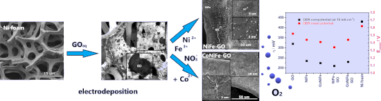
- ]. Afterwards, the current density tended to stabilize for NiFe and CoNiFe, which may be associated with the steady-state formation of the catalyst film on the metallic surface. The addition of cobalt to NiFe resulted in a lower overall current density during the synthesis process. In the case of the deposition
- reduction process of the already deposited GO. Afterwards, the current density increased due to the film formation, and then it gradually stabilized over time. A different chronoamperometric trend can be observed in the case of the electrodeposition of GO on the surface of nickel foam (Figure 1a inset). In


Quasi-guided modes resulting from the band folding effect in a photonic crystal slab for enhanced interactions of matters with free-space radiations
Beilstein J. Nanotechnol. 2023, 14, 322–328, doi:10.3762/bjnano.14.27

- larger than that of most plasmonic nanoantennas, suggesting the great potential of these QGMs for enhanced light–matter interactions. We use GMs supported by a regular PCS structure composed of a square lattice of air holes perforating a thin silicon (refractive index: 3.45) film on a silica (refractive


Spin dynamics in superconductor/ferromagnetic insulator hybrid structures with precessing magnetization
Beilstein J. Nanotechnol. 2023, 14, 233–239, doi:10.3762/bjnano.14.22

- film S that is in contact with a ferromagnetic insulator layer FI. Spin current and induced magnetization are calculated not only at the interface of the S/FI hybrid structure, but also inside the superconducting film. The new and interesting predicted effect is the frequency dependence of the induced
- interaction between the superconducting correlations and spin waves influences the dynamics of both superconducting and magnetic films. Interfacial exchange interaction between Cooper pairs and magnons results in a nonstationary induced magnetization and spin currents in the superconducting film and changes
- ][19] frameworks. However, the main subject of these works is the magnetic excitation spectrum in hybrid structures. Most of the works ignore the dynamics of nonuniform distributions of induced magnetization and spin current inside the superconducting film, which can be called the “dynamic inverse


A novel approach to pulsed laser deposition of platinum catalyst on carbon particles for use in polymer electrolyte membrane fuel cells
Beilstein J. Nanotechnol. 2023, 14, 190–204, doi:10.3762/bjnano.14.19

- ) number of electrons per O2 molecule formed during the ORR, (d) %H2O2 formed during the ORR. Curves (c) and (d) were calculated from the data in panels (a) and (b) using Equations 1 and 2, respectively, with η = 0.152 for 900 rpm. The thin film RRDE experiments were done in a four-electrode arrangement in


High–low Kelvin probe force spectroscopy for measuring the interface state density
Beilstein J. Nanotechnol. 2023, 14, 175–189, doi:10.3762/bjnano.14.18

- (Figure 1a). No oxide film on the semiconductor surface is assumed, and to simplify the discussion, the CPD between the tip and the semiconductor substrate is assumed to be zero. To investigate the electrostatic force acting between the tip and the semiconductor surface, we use the theoretical model


Structural, optical, and bioimaging characterization of carbon quantum dots solvothermally synthesized from o-phenylenediamine
Beilstein J. Nanotechnol. 2023, 14, 165–174, doi:10.3762/bjnano.14.17

- 2.2 mg/mL. These specimens were designated as CQDs/PU. For bioimaging studies, toluene was evaporated, and a thin film of CQDs was redissolved in water and filtered. The prepared QCD samples were characterized by transmission electron microscopy (TEM), atomic force microscopy (AFM), Fourier


Formation of nanoflowers: Au and Ni silicide cores surrounded by SiOx branches
Beilstein J. Nanotechnol. 2023, 14, 133–140, doi:10.3762/bjnano.14.14

- substrate at higher temperatures in oxygen-deficient environment [3][4]. Another cost-effective nanofabrication method, thin film dewetting, driven by the reduction of the surface energy and the interface energy has also been profusely studied because it provides a straightforward and fast way to produce
- nanoparticles [5][6][7]. The research of thin film dewetting has been extended to bilayers and multilayers for the synthesis of multicomponent nanoparticles [8][9][10][11][12][13][14][15][16], like alloyed AuNi and AuAg nanoparticles produced by the solid-state dewetting of bilayers [17][18][19][20][21][22][23
- small pieces were ready for thin film deposition. Metallic bilayers of Au and Ni of three different thickness ratios and a total thickness of 20 nm were deposited onto the SiO2/Si substrate by electron beam evaporation (CS400ES, VON ARDENNE) at a working pressure of 1 × 10⁻⁶ mbar. The Au layer was


Characterisation of a micrometer-scale active plasmonic element by means of complementary computational and experimental methods
Beilstein J. Nanotechnol. 2023, 14, 110–122, doi:10.3762/bjnano.14.12

- software COMSOL Multiphysics has been used to predict and confirm the dynamic temperature distribution and the optical response of the system. Experimental The manufacturing of the active plasmonic elements employed in the present work is detailed in [5]. At first, a 48 ± 2 nm film of silver is deposited
- on a sapphire substrate via physical vapour deposition (PVD). After this, two separate AFMs are used to machine channels in the silver film to create the desired constriction, which in this case measures 10 μm. The tip of the AFM is held at a set loading force in contact with the thin metal film and
- constriction in the silver film such that a current modulated at a particular frequency affects its optical properties via Joule heating. The signal is acquired by a photodiode and further processed by a lock-in amplifier (Ametek 5210), with the driving signal of the modulated voltage acting as reference. The


Antimicrobial and mechanical properties of functionalized textile by nanoarchitectured photoinduced Ag@polymer coating
Beilstein J. Nanotechnol. 2023, 14, 95–109, doi:10.3762/bjnano.14.11

- nanocomposites are prepared via ex situ or in situ approaches, in which MNPs are either synthesized beforehand and subsequently added to a polymer matrix or directly generated inside the polymer film. Ex situ methods include grafting [34], electrostatic [35] or polyol processes [36], but remain relatively
- difficult to implement and tend to cause NP self-aggregation. In situ methods are therefore generally preferred and typically require the polymer film surface to be treated with a metal precursor solution (layer-by-layer [37][38], sol–gel [39]) before undergoing thermal [40] or chemical reduction reactions
- increases with exposure time, which indicates an increase in NP concentration. Since the absorption peak is 426 nm for the Ag@PEG600DA/PETIA coating, the particles are expected to be slightly smaller than those of the Ag@PEG600DA film. This can be explained by the fact that the PETIA comonomer is a


Combining physical vapor deposition structuration with dealloying for the creation of a highly efficient SERS platform
Beilstein J. Nanotechnol. 2023, 14, 83–94, doi:10.3762/bjnano.14.10

- complexity and the high cost of gold restrict its use in devices. Here, we report on a novel two-step approach that combines the deposition of a silver–aluminum thin film with dealloying to design and fabricate efficient SERS platforms. The magnetron sputtering technique was used for the deposition of the
- alloy thin film to be dealloyed. After dealloying, the resulting silver nanoporous structures revealed two degrees of porosity: macroporosity, associated to the initial alloy morphology, and nanoporosity, related to the dealloying step. The resulting nanoporous columnar structure was finely optimized by
- rhodamine B. Keywords: dealloying; magnetron sputtering; nanoporous thin film; nanostructuring; SERS; Introduction Pollutant residues are strictly regulated in most countries to ensure water and food safety. In this context, there is an increasing demand for pollutant analysis tools with practical and


Upper critical magnetic field in NbRe and NbReN micrometric strips
Beilstein J. Nanotechnol. 2023, 14, 45–51, doi:10.3762/bjnano.14.5

- the electrical resistivity [6]. This feature is related to the polycrystalline or amorphous nature of these materials when deposited in a thin-film form [4][7][8]. In addition to the applicative interest, the study of these materials is relevant from a fundamental point of view. NbxRe1−x (NbRe) for


Gap-directed chemical lift-off lithographic nanoarchitectonics for arbitrary sub-micrometer patterning
Beilstein J. Nanotechnol. 2023, 14, 34–44, doi:10.3762/bjnano.14.4

- to etch the exposed underlying Au film. After 30 min of etching, the substrate was rinsed with deionized water and blown dry with nitrogen gas. The transferred metal structures were then characterized by optical microscopy, scanning election microscopy (SEM, JEOL JSM-7600F, Tokyo, Japan) and atomic


The influence of structure and local structural defects on the magnetic properties of cobalt nanofilms
Beilstein J. Nanotechnol. 2023, 14, 23–33, doi:10.3762/bjnano.14.3

- contacts [35], which are successfully implemented in memory and information storage devices. A similar layered heterostructure, but with the addition of a thin platinum film necessary for the generation of spin–orbit bonds, is also described in [36]. Comprehensive research on new promising materials is a
- behavior of the target film heterostructure, the absence of a magnetic field is observed inside the metal, which is predominantly concentrated near the surface. For the reasons previously described, niobium nanofilms were excluded from explicit consideration in numerical experiments to investigate the
- dimensions as the ideal HCP structure in the first numerical experiment. A group of cobalt atoms with structural defects acquired as a result of film sputtering in an enlarged form is shown in Figure 3b. Henceforward, to simplify the formulation, the nanosystem of cobalt atoms from the numerical experiment


Electrical and optical enhancement of ITO/Mo bilayer thin films via laser annealing
Beilstein J. Nanotechnol. 2022, 13, 1589–1595, doi:10.3762/bjnano.13.133

- to improve the performance of optoelectronic devices. One of these materials is indium tin oxide (ITO), which combines high transparency with high conductivity [7][8]. However, a single layer of as-deposited ITO shows a high resistivity. Consequently, inserting a very thin metal film layer can
- annealing, a laser beam irradiates the surface layer of the thin film without causing damage. The temperature increases quickly during the process within a short period [24][27]. The laser beam must have a uniform intensity with asymmetrical distribution to obtain surfaces of good morphology with low
- plasma cleaner. In the IM structure, the thickness of ITO was 125 nm while the thickness of Mo was 10 nm. The thickness was controlled by two quartz crystal balances integrated within the chamber. After deposition, the bilayer thin film was treated using a Nd:YAG pulsed laser with a wavelength of 1064 nm


Observation of collective excitation of surface plasmon resonances in large Josephson junction arrays
Beilstein J. Nanotechnol. 2022, 13, 1578–1588, doi:10.3762/bjnano.13.132

- consists of a log-periodic microwave antenna [39] with a broad frequency range of ca. 15–700 GHz. In the center, there is a nanoscale JJ sensor, shown in Figure 6b. The detector is made of a Nb film (70 nm thick), using a fabrication technique similar to that described in [28]. The antenna is patterned


Single-step extraction of small-diameter single-walled carbon nanotubes in the presence of riboflavin
Beilstein J. Nanotechnol. 2022, 13, 1564–1571, doi:10.3762/bjnano.13.130

- properties [3][4][5]. Moreover, as-synthesized SWCNTs typically possess a wide range of diameters and chiralities, leading to an inhomogeneous distribution of optical and electronic properties [5]. Nevertheless, most SWCNT applications, including thin-film electronics, require individual constituent parts


Utilizing the surface potential of a solid electrolyte region as the potential reference in Kelvin probe force microscopy
Beilstein J. Nanotechnol. 2022, 13, 1558–1563, doi:10.3762/bjnano.13.129

- the reduction of Ti ions in the solid electrolyte owing to direct contact between the Li metal and solid electrolyte, a poly(ethylene oxide)-based polymer electrolyte film (Osaka Soda Co., Ltd.), denoted PEO, was inserted between them. Before the KPFM measurements, the sample was heated at 150 °C for
- oxide)-based polymer electrolyte film, denoted PEO, is inserted between the metallic Li and the solid electrolyte to avoid reduction of Ti ions. A DC voltage is applied between the two Au electrodes. The left Au electrode (Au1) potential relative to the metallic Li electrode (vs Li+/Li) is measured
- , shown in Figure 1. Potential of Au1 and Au2 electrodes relative to the Li reference electrode at each applied DC voltage during the KPFM measurements. Acknowledgements We thank Osaka Soda Co., Ltd. for the supply of the polymer electrolyte film. Funding This work was partially supported by the


