Search results
Search for "diamond" in Full Text gives 213 result(s) in Beilstein Journal of Nanotechnology. Showing first 200.
Friction force microscopy of tribochemistry and interfacial ageing for the SiOx/Si/Au system
Beilstein J. Nanotechnol. 2018, 9, 1647–1658, doi:10.3762/bjnano.9.157

- passivating Si(100), as we did not find any wear debris on the tips or on the surfaces. Wear rates of sharp AFM tips after sliding distances of up to 1 μm against diamond have been calculated earlier [24]. The wear volumes and sliding distances were much smaller than in our experiments but the wear rates of


Interaction-tailored organization of large-area colloidal assemblies
Beilstein J. Nanotechnol. 2018, 9, 1582–1593, doi:10.3762/bjnano.9.150

- (diallyldimethylammonium chloride) (PDDA, MW 200000–350000), poly(sodium 4-styrenesulfonate) (PSS, MW 70000) and poly(allylamine hydrochloride) (PAH, MW 50000) were purchased from Sigma-Aldrich. Methods The substrates were cut with a diamond tip into squares with an area of about 1 cm2 and cleaned in acetone and


Correlative electrochemical strain and scanning electron microscopy for local characterization of the solid state electrolyte Li1.3Al0.3Ti1.7(PO4)3
Beilstein J. Nanotechnol. 2018, 9, 1564–1572, doi:10.3762/bjnano.9.148

- ground for 10 to 15 minutes at 150 rpm. This was followed by polishing the samples for 4 to 8 minutes at 300 rpm in four steps. In the first two steps, a diamond suspension with 3 µm and 2 µm particles was used. Finally, two finishing steps were performed with a 0.2 µm silica suspension and a 0.05 µm


Formation mechanisms of boron oxide films fabricated by large-area electron beam-induced deposition of trimethyl borate
Beilstein J. Nanotechnol. 2018, 9, 1282–1287, doi:10.3762/bjnano.9.120

- structural properties similar to those of tetraethyl orthosilicate (TEOS, Si(C2H5O)4), which has been well characterized as a precursor for EBID of silica films [14]. TMB has previously been used for boron doping of SiO2 [15] and diamond [16], and the deposition of BCN fibres [17], BN nanotubes [18] and BN


Room-temperature single-photon emitters in titanium dioxide optical defects
Beilstein J. Nanotechnol. 2018, 9, 1085–1094, doi:10.3762/bjnano.9.100

- types of single-photon emitters that include molecules [3], trapped atoms [4], quantum dots [5] and defects in diamond [6]. More recently point defects of wide-bandgap semiconductors, such as zinc oxide (ZnO) [7][8][9] and silicon carbide [10], were shown to exhibit room-temperature single-photon


Review on nanoparticles and nanostructured materials: history, sources, toxicity and regulations
Beilstein J. Nanotechnol. 2018, 9, 1050–1074, doi:10.3762/bjnano.9.98

- during space missions and meteorite collections determined that the vast assortment of carbide, oxide, nitride, silicate, carbon, and organic-based NMs are the main components of stardust [44]. Diamond, of a few nanometers in diameter, has been observed in the Murchison meteorite, which is a perfect


Cyclodextrin inhibits zinc corrosion by destabilizing point defect formation in the oxide layer
Beilstein J. Nanotechnol. 2018, 9, 936–944, doi:10.3762/bjnano.9.86
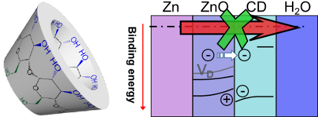
- microscope. The samples were irradiated with an excitation wavelength of 532.1 nm/2.33 eV through a microscope objective of 100× magnification and with a numerical aperture of 0.75. In situ spectroscopic ellipsometry (SE) was performed on Zn samples polished down to a 1 μm diamond suspension. Experiments


Heavy-metal detectors based on modified ferrite nanoparticles
Beilstein J. Nanotechnol. 2018, 9, 762–770, doi:10.3762/bjnano.9.69

- Nicolet 6700 spectrometer working in transmission mode as a series of 32 repetitive runs. Here, a small amount of powder was directly placed and squeezed into a diamond window for measurement. Mössbauer spectra (MS) were obtained in constant acceleration mode with a 57Co in Cr matrix source. The spectra


Tuning adhesion forces between functionalized gold colloidal nanoparticles and silicon AFM tips: role of ligands and capillary forces
Beilstein J. Nanotechnol. 2018, 9, 660–670, doi:10.3762/bjnano.9.61

- (blue). a) Adhesion values between silicon tip and functionalized Au NPs measured with Peakforce QNM AFM as a function of Au NPs diameter and functionalization: orange triangle –SH, blue circle –NH2, red circle –OCH3, green triangle –OH, black diamond –CH3, brown triangle –COOH end-groups; b) zoom in on


Engineering of oriented carbon nanotubes in composite materials
Beilstein J. Nanotechnol. 2018, 9, 415–435, doi:10.3762/bjnano.9.41

- future outlook. Keywords: arrangement and alignment; carbon nanotubes; composite materials; orientation; Review Introduction Carbon is one of the most abundant elements comprising the world around us. Before 1985 graphite and diamond were the only known structural forms of carbon [1]. In 1991, Iijima


Design of polar self-assembling lactic acid derivatives possessing submicrometre helical pitch
Beilstein J. Nanotechnol. 2018, 9, 333–341, doi:10.3762/bjnano.9.33

- (blue triangle) and KL 4/6 (cyan diamond) as indicated. Temperature dependencies of the helix pitch length p for KL 3/4 (black rectangle), KL 3/5 (red cicle), KL 4/4 (green triangle), KL 4/5 (blue triangle) and KL 4/6 (cyan diamond) as indicated. 3D plots of the imaginary part of complex permittivity


Review: Electrostatically actuated nanobeam-based nanoelectromechanical switches – materials solutions and operational conditions
Beilstein J. Nanotechnol. 2018, 9, 271–300, doi:10.3762/bjnano.9.29

- repetitive on–off switching. An AFM-based study on the nanoscale wear of diamond-like carbon against and ultra-nanocrystalline diamond showed that the surface wear increases the size of the contact by gradually removing atoms at discrete sites and is a thermally activated stress-assisted process [79]. This
- our knowledge, the highest durability (106 on/off cycles, 10 ns response time) of a 2T CNT-based switch was demonstrated by Loh et al. for carbon–carbon contacts, using multiwall CNT as a switching element and diamond-like carbon (DLC) as a contact material [12]. However, the reported actuation


Bombyx mori silk/titania/gold hybrid materials for photocatalytic water splitting: combining renewable raw materials with clean fuels
Beilstein J. Nanotechnol. 2018, 9, 187–204, doi:10.3762/bjnano.9.21

- mold, covered with resin, and treated at 60 °C for 24 h. After cooling to room temperature, the embedded samples were trimmed and sectioned (100 nm nominal slice thickness, Leica Ultracut UCT with diamond knife at room temperature). Transmission electron microscopy (TEM) was done on a Philips CM 200
- infrared spectroscopy (FT-ATR-IR) was done from 4000–500 cm−1 with a resolution of 2 cm−1 on an FT-IR NEXUS spectrometer with a ThermoNicolet SmartOrbit ATR attachment with a diamond crystal. Samples were directly deposited on the crystal und fixed in the measurement position via the SmartOrbit attachment


Dielectric properties of a bisimidazolium salt with dodecyl sulfate anion doped with carbon nanotubes
Beilstein J. Nanotechnol. 2018, 9, 164–174, doi:10.3762/bjnano.9.19

- ) [56][57], placed on untreated glass slides, using a Nikon 50iPol microscope equipped with a Linkam THMS600 hot stage and TMS94 control processor. Temperatures and enthalpies of transitions were recorded by using differential scanning calorimetry (DSC) technique employing a Diamond DSC Perkin Elmer


Design of photonic microcavities in hexagonal boron nitride
Beilstein J. Nanotechnol. 2018, 9, 102–108, doi:10.3762/bjnano.9.12

- ]. The former process is preferred when attempting to maximize the field overlap between the emitters and the cavity modes, and is often employed when using materials that are amenable to scalable nanofabrication protocols, such as gallium arsenide or silicon [17][18], and more recently diamond and


Response under low-energy electron irradiation of a thin film of a potential copper precursor for focused electron beam induced deposition (FEBID)
Beilstein J. Nanotechnol. 2018, 9, 57–65, doi:10.3762/bjnano.9.8

- reflection diamond crystal. Experimental setup in Orsay, France: The experiment setup at ISMO in Orsay, France is detailed in previous publications [29][36][46]. Samples are mounted on the cold finger of the cryostat and their temperature can be controlled from 30 K to 750 K. The temperature is measured with


Transition from silicene monolayer to thin Si films on Ag(111): comparison between experimental data and Monte Carlo simulation
Beilstein J. Nanotechnol. 2018, 9, 48–56, doi:10.3762/bjnano.9.7

- order of magnitude lower than the one measured for multilayer graphene [26]. Their structure slightly differs from the one of diamond, with an interlayer spacing 1% smaller than the one found between two consecutive hexagonal buckled planes in diamond-like bulk silicon, and a Raman peak also 1% shifted
- honeycomb-chained triangle (HCT) reconstruction observed on a Ag/Si(111) surface, it has been hypothesized that the observed films could result from the growth of diamond-like Si with Ag acting as a surfactant [28]. Such conclusions were also supported by low energy electron diffraction (LEED) [29][30
- ], ARPES [31] and grazing incidence X-ray diffraction [32]. The diamond-like structure of the film has been confirmed by scanning tunneling microscopy (STM) [33] and optical measurements [34]. The Ag termination of the surface has been also demonstrated by Auger electron spectroscopy (AES) [34], metastable


Gas-sensing behaviour of ZnO/diamond nanostructures
Beilstein J. Nanotechnol. 2018, 9, 22–29, doi:10.3762/bjnano.9.4

- -terminated nanocrystalline diamond (NCD) films and/or n-type ZnO nanorods (NRs) have been obtained via a facile microwave-plasma-enhanced chemical vapour deposition process or a hydrothermal growth procedure. The morphology and crystal structure of the synthesized materials was analysed with scanning
- : density functional theory (DFT); gas sensor; interdigital electrodes; nanocrystalline diamond; sensitivity; zinc oxide (ZnO); Introduction Currently, a number of studies have been focused on developing gas sensors based on nanomaterials and/or nanostructures. Metal oxides are the most common sensing
- oxides or noble metals [14][15][16][17]. Aside from n-type semiconductors, p-type semiconductor materials have also been extensively used for the detection of toxic gases [3][18][19]. Recently, nanocrystalline diamond (NCD) films have been utilized for advanced electronic devices because of their


Exploring wear at the nanoscale with circular mode atomic force microscopy
Beilstein J. Nanotechnol. 2017, 8, 2662–2668, doi:10.3762/bjnano.8.266

- volume) by subtracting relevant topographic images after and before wear. Finally, this methodology has been applied to a copper-based nanocomposite sample using both diamond-like carbon and silicon nitride tips in the µN load range. The results show that even if wear loss remains locally heterogeneous
- of the sliding time at a sliding velocity of 880 µm/s and a normal load of 1 µN (green squares) and 3 µN (red diamonds). Experiments were carried with a diamond-like carbon (DLC) probe. Error bars are the standard deviation and the data result from an average between the maximum wear volume and the


Patterning of supported gold monolayers via chemical lift-off lithography
Beilstein J. Nanotechnol. 2017, 8, 2648–2661, doi:10.3762/bjnano.8.265

- trimmed with a diamond scribe to ≈1 × 1 cm sample size. The substrates were annealed with a hydrogen flame and incubated in 1.0 mM ethanolic solutions of mercaptoundecanol overnight at room temperature and ambient pressure to form SAMs. The patterned PDMS stamps were treated with oxygen plasma (Harrick


Molecular dynamics simulations of nanoindentation and scratch in Cu grain boundaries
Beilstein J. Nanotechnol. 2017, 8, 2283–2295, doi:10.3762/bjnano.8.228

- diagrams used herein for analyzing the grain boundary properties (i.e., transverse grain boundary indentation, vertical grain boundary indentation, and vertical grain boundary scratches) are shown in Figure 1a–c, respectively. The indenter (blue) was made of a perfectly structured diamond while perfect


Material property analytical relations for the case of an AFM probe tapping a viscoelastic surface containing multiple characteristic times
Beilstein J. Nanotechnol. 2017, 8, 2230–2244, doi:10.3762/bjnano.8.223

- symbols show the analytical calculation based on Equation 30, which closely follows the results obtained from the simulation. The analytical solution specifically gives the amount of dissipated energy that is proportional to the storage modulus (first term in Equation 30, diamond symbols), the amount of


Angstrom-scale flatness using selective nanoscale etching
Beilstein J. Nanotechnol. 2017, 8, 2181–2185, doi:10.3762/bjnano.8.217

- . Subsequently, the molecules are dissociated by the ONF, and the dissociated radicals selectively etch the protrusions. Finally, the ONF disappears and the etching process stops automatically. Near-field etching is performed using Cl2 gas for glass, GaN [9], and plastic surfaces, and O2 gas for diamond and


A comparative study of the nanoscale and macroscale tribological attributes of alumina and stainless steel surfaces immersed in aqueous suspensions of positively or negatively charged nanodiamonds
Beilstein J. Nanotechnol. 2017, 8, 2045–2059, doi:10.3762/bjnano.8.205

- (2.29 ×10⁻¹⁹ g/5 nm particle) = 2 × 10⁻¹⁷ g. A surface coverage of 1010 clusters per cm2 therefore has a mass per unit area of ρ2 = 2 × 10⁻⁷ g/cm2, which corresponds to a decrease in the resonant frequency of 11.3 Hz (cf. Equation 3). For comparison, a monolayer of spherical 5 nm diamond nanoparticles
- packed in the closest hexagonal arrangement (assuming diamond bulk density of 3.5 g/cm3; mass per particle: 2.29 × 10⁻¹⁹ g) corresponds to 4.6 × 10¹² ND/cm2, ρ2 = 1.058 × 10⁻⁶ g/cm2 and a decrease in the resonant frequency of 59.8 Hz. Graphs of log(σ) vs log(scan size) obtained from the AFM images shown
- experiments. Thus, this observation is in agreement with Liu’s electrostatic hypothesis [9]. We note that recently an electrostatic self-assembly seeding of monosized individual diamond nanoparticles (obtained by a detonation method) on silicon dioxide surfaces has been reported [51]. Although the latter


Preparation and characterization of polycarbonate/multiwalled carbon nanotube nanocomposites
Beilstein J. Nanotechnol. 2017, 8, 2026–2031, doi:10.3762/bjnano.8.203

- the nanocomposites in nitrogen (flow rate 50 mL/min) from RT to 800 °C at a ramp rate of 10 °C/min. The TGA/DTA instrument was calibrated with standard weight indium standards for DTA heat flow. A differential scanning calorimetry (DSC) instrument (Pyris Diamond by Perkin Elmer, UK) was used to record


