Search results
Search for "fabrication" in Full Text gives 796 result(s) in Beilstein Journal of Nanotechnology. Showing first 200.
Ni, Co, Zn, and Cu metal-organic framework-based nanomaterials for electrochemical reduction of CO2: A review
Beilstein J. Nanotechnol. 2023, 14, 904–911, doi:10.3762/bjnano.14.74

- to the enhanced number of active sites achieved through the transition from the bulk state to the nanomaterial form. The optimal condition for the fabrication of 2D Ni(Im)2 was determined to be the utilization of 5 mL of NH4OH. Co-based MOFs nanomaterials Cobalt materials provide a diversity of
- converting individual MOFs into MOF-derived carbon-support nanomaterials. Another issue is the durability of the working electrodes. Many studies have employed drop casting and the use of binders to affix MOFs onto the substrate for electrode fabrication. This approach presents drawbacks such as reduced


Two-dimensional molecular networks at the solid/liquid interface and the role of alkyl chains in their building blocks
Beilstein J. Nanotechnol. 2023, 14, 872–892, doi:10.3762/bjnano.14.72

- related to energy and environment, among others. However, the fabrication of ordered nanoarchitectures remains a challenge, even in two dimensions. Therefore, a deeper understanding of the self-assembly processes and substantial factors for building ordered structures is critical for tailoring flexible
- and desirable nanoarchitectures. Scanning tunneling microscopy is a powerful tool for revealing the molecular conformations, arrangements, and orientations of two-dimensional (2D) networks on surfaces. The fabrication of 2D assemblies involves non-covalent interactions that play a significant role in
- -assembly; solid/liquid interface; two-dimensional networks; Introduction The fabrication of ordered nanostructures using the concept of nanoarchitectonics [1][2][3][4] for various applications such as nanomachines, nanoelectronics, catalysis, and nanopatterning remains challenging [5][6][7]. Design and


Industrial perspectives for personalized microneedles
Beilstein J. Nanotechnol. 2023, 14, 857–864, doi:10.3762/bjnano.14.70

- and disadvantages; for brevity, we encourage readers to access previous review papers that cover in depth light-based fabrication techniques [41][42][43]. SLA and DLP are by far the most common techniques for fabricating microneedles, with approximately eight times as many publications as publications
- volumetric throughput between DLP or SLA printers and 2PP instruments. In conjunction with new hardware, there have also been incremental changes in 2PP fabrication strategies. These strategies are based on voxel (volumetric pixel in x,y,z) control. Current 2PP software can be utilized to classify parts of
- internal photoresin. A third fabrication strategy leverages the combination of DLP and 2PP fabrication techniques. Sarker et al. [56] recently demonstrated the strength of combining fabrication techniques for microneedles. They used DLP to fabricate the bulky base and 2PP for microneedle fabrication, akin


Biomimetics on the micro- and nanoscale – The 25th anniversary of the lotus effect
Beilstein J. Nanotechnol. 2023, 14, 850–856, doi:10.3762/bjnano.14.69

- new research techniques and methodologies that enabled detailed investigation of biological archetypes. High-detail microscopy, analysis systems, and novel simulation tools helped to decode the secrets of nature, while new fabrication techniques helped to transfer these findings into technical
- were performed and the mandibles were analysed using (cryo-) scanning electron microscopy, indicating that a fluid substance covers the medial surface of the mandibles reducing propolis adhesion. Weiser et al. [13] take biomimetics into industrial production with their paper “Roll-to-roll fabrication
- tune and then scale up the fabrication of tools to handle nanofibres in industrial processes. Fibre–surface interactions are also the main theme in “Growing up in a rough world: scaling of frictional adhesion and morphology of the Tokay gecko (Gekko gecko)” by Cobos and Higham [15]. In the excitement


A wearable nanoscale heart sound sensor based on P(VDF-TrFE)/ZnO/GR and its application in cardiac disease detection
Beilstein J. Nanotechnol. 2023, 14, 819–833, doi:10.3762/bjnano.14.67

- electrospinning were controlled at 25 °C and 40% RH, respectively. Fabrication of wearable flexible nanoscale heart sound sensors Figure 2 illustrates the process of creating a wearable, flexible nanoscale heart sound sensor with a sandwich structure. First, a rectangular composite nanofilm measuring 4.5 cm in


Silver-based SERS substrates fabricated using a 3D printed microfluidic device
Beilstein J. Nanotechnol. 2023, 14, 793–803, doi:10.3762/bjnano.14.65

- fabrication, resulting in a low aspect ratio of the achieved features. Because 3D printing enables the creation and testing of objects in short periods of time, it provides a new tool for constructing microfluidic devices. This has led to fast and dynamic developments in chemical synthesis and analytical
- systems at low cost [24][25][26]. There are two techniques for producing 3D-printed microfluidic devices. In the first approach, monolithic microfluidic devices are 3D printed [27][28]. Although this one-step process offers the benefits of quick development and ease of fabrication, reducing the channel
- , TESCAN). A UV–vis spectrometer (Agilent 8453, Agilent, USA) and a micro-Raman spectrometer (NS200, Nanoscope System, Republic of Korea) were used to record the absorption spectra and Raman spectra, respectively. Fabrication of the droplet-based microfluidic device The fabrication process of the


Carboxylic acids and light interact to affect nanoceria stability and dissolution in acidic aqueous environments
Beilstein J. Nanotechnol. 2023, 14, 762–780, doi:10.3762/bjnano.14.63

- structures. The authors thank Marsha Ensor for her contribution. This report is based on the following: Hancock, M. L. The Fabrication and Characterization of Metal Oxide Nanoparticles Employed in Environmental Toxicity and Polymeric Nanocomposite Applications. Doctoral Dissertation, University of Kentucky

In situ magnesiothermic reduction synthesis of a Ge@C composite for high-performance lithium-ion batterie anodes
Beilstein J. Nanotechnol. 2023, 14, 751–761, doi:10.3762/bjnano.14.62

- from Binh Dinh province, Vietnam. Fabrication of activated carbon from banana peel A procedure similar to our previous work [33] has been used to prepare carbon materials from banana peels. An appropriate amount of banana peels was dried at 80 °C overnight in a vacuum oven and ground into small pieces
- ) water, before being dried in a vacuum oven at 110 °C for 12 h. The product was further heated under air at 300 °C for 3 h. The activated carbon was obtained after washing with 2 M HCL and DI water. It was dried under vacuum and denoted as BC-800. In situ fabrication of Ge/C-iM750 composite material A


Control of morphology and crystallinity of CNTs in flame synthesis with one-dimensional reaction zone
Beilstein J. Nanotechnol. 2023, 14, 741–750, doi:10.3762/bjnano.14.61

- properties in terms of morphology, size, type, and functionalization have been reported [2]. Controlling the properties of nanotubes is essential for various applications. In a recent study on the production of CNT-based conductive textiles, the fabrication of conductive wool required the utilization of


Nanoarchitectonics for advanced applications in energy, environment and biology: Method for everything in materials science
Beilstein J. Nanotechnol. 2023, 14, 738–740, doi:10.3762/bjnano.14.60
- nanotechnology, which pioneered the science at that length scale. Such methodologies were also touched upon in the bottom-up fabrication of materials using supramolecular chemistry and other methods [7][8]. Nanoarchitectonics encompasses these methods and integrates them into a broader field of research
- that include the word “nanoarchitectonics” in the title, one would appreciate that these manuscripts are not only coming from basic fields of research such as material fabrication [12][13], structural control [14][15], elucidation of physical phenomena [16][17], and basic bio-related sciences [18][19

A graphene quantum dots–glassy carbon electrode-based electrochemical sensor for monitoring malathion
Beilstein J. Nanotechnol. 2023, 14, 701–710, doi:10.3762/bjnano.14.56

- expertise. It is therefore necessary to develop a technology that can detect pesticides quickly, easily, and economically. With electrochemical detection techniques, a wide range of pesticides can be detected by the fabrication of simple, cost-effective, rapid, and high-throughput portable devices [8]. The
- collected after centrifugation. To obtain the GQDs, the final black suspension was filtered through a 0.22 µm syringe filter. Fabrication of the electrochemical sensor A mirror-like surface was first achieved on the bare GCE by polishing it with 0.3 and 0.05 μm alumina powder. In the next step the GCE was
- malathion detection (Figure 10). Conclusion Graphene quantum dots (size range 5 to 40 nm) were chemically synthesized by using glucose as a precursor in a hydrothermal method. This paper describes the fabrication of an electrochemical nanosensor by modifying a bare glassy carbon electrode with GQDs. The


Metal-organic framework-based nanomaterials as opto-electrochemical sensors for the detection of antibiotics and hormones: A review
Beilstein J. Nanotechnol. 2023, 14, 631–673, doi:10.3762/bjnano.14.52

- materials as potent analytical tools because of their advantages in terms of portability, affordability, high sensitivity, and ease of fabrication. Through functions such as active large surface area, rapid electrode kinetics, and efficient catalytic activity, the amplification of electrochemical signals


Titania nanoparticles for photocatalytic degradation of ethanol under simulated solar light
Beilstein J. Nanotechnol. 2023, 14, 616–630, doi:10.3762/bjnano.14.51

- differences could promote the fabrication of new devices with higher efficiency in electron–hole separation [33]. There are a lot of methods to obtain TiO2 powder, from chemical reactions in solvents [34][35][36] to simple oxidation at high temperatures [37]. Every method has its particular yield and


ZnO-decorated SiC@C hybrids with strong electromagnetic absorption
Beilstein J. Nanotechnol. 2023, 14, 565–573, doi:10.3762/bjnano.14.47

- properties of the SCZ samples is discussed in detail. Experimental Preparation of SiC@C nanowires The synthesis of SiC@C was described in our previous work [24]. The synthesis temperature has been fixed to 800 °C for 1 h for the carbonization of SiCnw. Fabrication of SiC@C-ZnO hybrids Different amounts of
- carbon and wax). These findings suggest that SiC@C-ZnO hybrids with diverse microstructures may have a bright future as EM absorbers. Conclusion A new strategy for the controllable fabrication of SiC@C-ZnO hybrids via carbonization and hydrolysis reaction is described. Morphology and permittivity of the


SERS performance of GaN/Ag substrates fabricated by Ag coating of GaN platforms
Beilstein J. Nanotechnol. 2023, 14, 552–564, doi:10.3762/bjnano.14.46

- University of Technology, gen. Sylwestra Kaliskiego 2, 00-908 Warsaw, Poland Institute of Optoelectronics, Military University of Technology, gen. Sylwestra Kaliskiego 2, 00-908 Warsaw, Poland 10.3762/bjnano.14.46 Abstract The results of comparative studies on the fabrication and characterization of GaN/Ag
- ][22]. Due to the easiness of fabrication, the most extensively studied SERS substrates are those based on metallic nanoparticles and their assemblies [21][22]. Among SERS substrates fabricated using physical methods of particular interest are those based on nanostructured GaN platforms coated with
- physical vapor deposition (PVD) methods have been tested to replace MS in coating GaN platforms with plasmonic metals. Pulsed laser deposition (PLD) is an interesting and still not fully explored alternative for the fabrication of SERS substrates [37][38]. Hence, our studies reported herein aimed to


Observation of multiple bulk bound states in the continuum modes in a photonic crystal cavity
Beilstein J. Nanotechnol. 2023, 14, 544–551, doi:10.3762/bjnano.14.45

- influenced by both the radiative part Qr and a nonradiative part Qnr via 1/Q = 1/Qr + 1/Qnr provided that the material is lossless. Qnr incorporates defects such as structural disorder, surface roughness, and fabrication errors. The simulation of the unit cell was performed by COMSOL Multiphysics with
- Leff larger. Consequently, the M33 mode in the reciprocal space is closer to the Г point than the M14/41 modes. For mode indices larger than M14/41, mode leakage becomes more significant, resulting in Q factor degradation of the corresponding higher-order bulk modes. Sample fabrication and measurement
- fabrication disorders on each mode. The close eigenwavelength values of the resonances in Figure 4c make the Qr degradation difference negligible, but the structural disorders (non-symmetry, tilted angle, and center shift of the structure) have a distinct impact on the different modes. If the structural


Nanoarchitectonics to entrap living cells in silica-based systems: encapsulations with yolk–shell and sepiolite nanomaterials
Beilstein J. Nanotechnol. 2023, 14, 522–534, doi:10.3762/bjnano.14.43

- Biological Sciences, Complutense University of Madrid (UCM), C/ José Antonio Novais 12, 28040 Madrid, Spain 10.3762/bjnano.14.43 Abstract In the present work, the bottom-up fabrication of biohybrid materials using a nanoarchitectonics approach has been applied to entrap living cells. Unicellular
- biological functions that can be effectively manipulated through the inorganic components, with potential impact on leading applications within the fields of chemical synthesis and catalysis, energy, environment, and biomedicine. Examples of bionanohybrids include the bottom-up fabrication of


Microneedle patches – the future of drug delivery and vaccination?
Beilstein J. Nanotechnol. 2023, 14, 494–495, doi:10.3762/bjnano.14.40
- ][9]. Recent progress may be broadly categorised as MN design, fabrication, skin penetration studies, and applications, ranging from drug delivery and vaccination to diagnostics. The first two of these have received most attention, but considerable work is still to be done in all categories – more in
- vivo studies for example. In the meantime, progress towards large-scale manufacture of moulded polymer MNs is progressing at pace, with the aid of new advanced 3D mould fabrication tools [10]. This special edition provides a snapshot of current research into MNs and their applications. It focuses on
A mid-infrared focusing grating coupler with a single circular arc element based on germanium on silicon
Beilstein J. Nanotechnol. 2023, 14, 478–484, doi:10.3762/bjnano.14.38

- couplers requiring secondary etching, the proposed full-etch grating coupler structure can reduce the complexity of fabrication and can provide a prospective platform for MIR photonic integration and photonic biosensor detection. Keywords: circular arc element; focusing grating coupler; germanium-on
- membrane Ge waveguide [1]. The maximum coupling efficiency was −11 dB at the focusing SWG’s center wavelength of 2.37 μm. The high coupling efficiency was obtained experimentally. However, the fabrication flow of the suspended membrane Ge waveguide with focusing SWGs greatly increased the complexity of the
- technological process. Therefore, a focusing grating coupler (FGC) with a simple fabrication process and high coupling efficiency is urgently needed. In this paper, a MIR FGC with a single circular arc element (CAE) based on Ge-on-Si is demonstrated and simulated. The proposed MIR FGC consists of a section of


Conjugated photothermal materials and structure design for solar steam generation
Beilstein J. Nanotechnol. 2023, 14, 454–466, doi:10.3762/bjnano.14.36

- THF solution and (c) for drop-cast films. (d) The photoluminescence (PL) spectra of the DPP derivatives in THF solution. (Figure 4 was adapted with permission from [27], Copyright 2021 American Chemical Society.) Typical polymeric PTMs used for SSG. (a) Schematic illustration of the fabrication
- Energy Conversion”, Adv. Mater., with permission from John Wiley and Sons. Copyright © 2019 WILEY-VCH Verlag GmbH & Co. KGaA, Weinheim. This content is not subject to CC BY 4.0. (a) Schematic illustration of the fabrication process and characterization of the photothermal p-PEGDA−PANI hydrogel. (b) Solar
- , Copyright (2021), with permission from Elsevier. This content is not subject to CC BY 4.0. Fabrication process of PPy nanofiber light-trapping coatings by ultrasonic spray coating. (Figure 9 was reproduced with permission from [29], Copyright 2021 American Chemical Society). Surface morphology of (a) filter


Molecular nanoarchitectonics: unification of nanotechnology and molecular/materials science
Beilstein J. Nanotechnol. 2023, 14, 434–453, doi:10.3762/bjnano.14.35

- , fabrication engineering, and bio-related science (Figure 1) [51][52]. Materials synthesis by nanoarchitectonics is envisioned to integrate and use various processes [53]. For example, physical/chemical material transformation, atomic/molecular manipulation, self-assembly/self-organization, arrangement and
- everything in materials science [90], analogous to the theory of everything in physics [91]. Nanoarchitectonics is a highly universal concept. Therefore, the fabrication of structures from molecules to materials that has been done so far can also be considered part of the nanoarchitectonics processes. Here
- synthesis are usually difficult to incorporate into functional nanodevices because of the random arrangement of the heterojunctions. Bronner, Fischer, Crommie, and co-workers have developed a single hierarchical fabrication strategy via on-surface synthesis of graphene nanoribbons with a single


Evaluation of electrosynthesized reduced graphene oxide–Ni/Fe/Co-based (oxy)hydroxide catalysts towards the oxygen evolution reaction
Beilstein J. Nanotechnol. 2023, 14, 420–433, doi:10.3762/bjnano.14.34
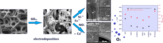
- was the structure of NiFe and the electroactive surface area of GO. Experimental Fabrication of the catalysts NiFe and CoNiFe oxides/(oxy)hydroxides were synthesized in a one-step process by electrodeposition at −1.1 V vs Ag/AgCl in an aqueous solution of 4 mM nickel(II) nitrate hexahydrate (Ni(NO3)2
- Gaussian–Lorentzian (GL30) curve as a fitting algorithm and a Shirley background subtraction. Electrochemical studies The setup for the electrochemical studies was the same as for the fabrication of the catalysts (see section “Electrosynthesis and morphology of the deposits”) with some exceptions: The


Plasmonic nanotechnology for photothermal applications – an evaluation
Beilstein J. Nanotechnol. 2023, 14, 380–419, doi:10.3762/bjnano.14.33


Polymer nanoparticles from low-energy nanoemulsions for biomedical applications
Beilstein J. Nanotechnol. 2023, 14, 339–350, doi:10.3762/bjnano.14.29

- research on the fabrication of polymer nanoparticles from low-energy nanoemulsions, focusing on phase inversion composition. We particularly emphasize their biomedical applications as drug carriers. 2 Nanoemulsions Nanoemulsions are constituted by nanoscale droplets (20–200 nm) dispersed in a continuous


Bismuth-based nanostructured photocatalysts for the remediation of antibiotics and organic dyes
Beilstein J. Nanotechnol. 2023, 14, 291–321, doi:10.3762/bjnano.14.26

- covered. The creation of Z-schemes, Schottky junctions, and heterojunctions, as well as morphological modifications, doping, and other processes are highlighted regarding the fabrication of bismuth-based photocatalysts with improved photocatalytic capabilities. A discussion of general photocatalytic


