Search results
Search for "post-processing" in Full Text gives 56 result(s) in Beilstein Journal of Nanotechnology.
Laser–material interactions in liquids for the synthesis of nanomaterials: current status and perspectives
Beilstein J. Nanotechnol. 2026, 17, 571–575, doi:10.3762/bjnano.17.38

- and post-processing steps. To fully realize this potential, the field must transition from laboratory-scale demonstrations to scalable industrial processes. Achieving this goal will require continued advances in fundamental understanding, integration of computational and experimental tools, and
Beam shaping techniques for pulsed laser ablation in liquids: Unlocking tunable control of nanoparticle synthesis in liquids
Beilstein J. Nanotechnol. 2026, 17, 309–342, doi:10.3762/bjnano.17.22


Mechanical property measurements enabled by short-term Fourier-transform of atomic force microscopy thermal deflection analysis
Beilstein J. Nanotechnol. 2025, 16, 1952–1962, doi:10.3762/bjnano.16.136

- (Nanosensors PtSi-CONT), and borosilicate glass colloids (Sigma-Aldrich 440345-100G) attached to the tipless cantilevers (Nanosensors TL-CONT). The borosilicate glass colloids had a diameter of 8–11 μm and an elastic modulus of 60 GPa. Data analysis Following completion of experiments, post processing of the


Ambient pressure XPS at MAX IV
Beilstein J. Nanotechnol. 2025, 16, 1677–1694, doi:10.3762/bjnano.16.118

- observed when comparing the data measured with the two acquisition techniques in Figure 6. The spectroscopic changes induced by the modulation can often be directly seen in pump–probe data, while post-processing is necessary for continuous measurements to obtain similar information. Examples of the two


Bioinspired polypropylene-based functionally graded materials and metamaterials modeling the mistletoe–host interface
Beilstein J. Nanotechnol. 2025, 16, 1592–1606, doi:10.3762/bjnano.16.113

- applied. The small deviation may be due to the volume reduction of PP during hot pressing, the burnt glass fibers at the edges, and inaccuracies in the post-processing threshold algorithms. The good fusion of the individual compartments and the gradual increase in fiber concentration along the specimen


Laser processing in liquids: insights into nanocolloid generation and thin film integration for energy, photonic, and sensing applications
Beilstein J. Nanotechnol. 2025, 16, 1428–1498, doi:10.3762/bjnano.16.104

- laser irradiation to fragment larger NPs suspended in a colloidal solution, resulting in smaller NPs with a narrow size distribution. LFL is particularly beneficial as a post-processing tool for NPs produced by PLAL, a technique which often results in broader or bimodal size distributions as discussed
- in the previous section. Unlike traditional post-processing methods such as centrifugation or salinity size quenching, LFL provides a cost-effective and efficient alternative. It excels at producing ultrasmall NPs with diameters below 5 nm and sub-nanometer atomic clusters, which have significant


Crystalline and amorphous structure selectivity of ignoble high-entropy alloy nanoparticles during laser ablation in organic liquids is set by pulse duration
Beilstein J. Nanotechnol. 2025, 16, 1141–1159, doi:10.3762/bjnano.16.84

- ]. Those rules are very high cooling rates, the presence of at least three constituting elements, atomic size differences over 12%, a significant negative heat of mixing of major elements, small material dimensions (preferably at the nanoscale, favoring high cooling rates), and post-processing effects
- . Consequently, the number of laser pulses per particle changes with ablation time. A previous study by Su et al. shows amorphization of nanoparticles after laser post-processing [78], indicating a potential interplay between amorphization and post-irradiation. To understand whether the amorphous phase formation


Changes of structural, magnetic and spectroscopic properties of microencapsulated iron sucrose nanoparticles in saline
Beilstein J. Nanotechnol. 2025, 16, 762–784, doi:10.3762/bjnano.16.59


Enhancing mechanical properties of chitosan/PVA electrospun nanofibers: a comprehensive review
Beilstein J. Nanotechnol. 2025, 16, 286–307, doi:10.3762/bjnano.16.22

- hydrophilicity, and low thermal stability [106][107]. The disadvantages often necessitate the combination of PVA with other materials or the application of post-processing techniques such as cross-linking or coating for performance improvement [108]. As a countermeasure, Rafieian et al. [109] proposed


Modeling and simulation of carbon-nanocomposite-based gas sensors
Beilstein J. Nanotechnol. 2025, 16, 90–96, doi:10.3762/bjnano.16.9

- settings for time-dependent and stationary analyses. In the solving phase, simulations are executed to generate results, followed by post-processing to analyse and present the outcomes in 1D and 3D plots. The sensor layer where the adsorption of the gas occurs and thus participate in detecting the CO gas


A biomimetic approach towards a universal slippery liquid infused surface coating
Beilstein J. Nanotechnol. 2024, 15, 1376–1389, doi:10.3762/bjnano.15.111

- Innova instrument in tapping mode. RTESPA-300 (Bruker, Billerica, MA) probes were used with a tip radius of 12 nm, a spring constant of 40 N/m, and a frequency of 300 kHz. A minimum of six images from two different samples were produced with dimensions of 5 × 5 μm at a scan rate of 0.5 Hz. Post
- processing and analysis of the collected scans included a lowpass filter and took place in the “NanoScope analysis” software. Sum frequency generation vibrational spectroscopy The SFG setup used an EKSLPA Nd:YAG laser operated at 50 Hz to generate a fixed visible (532 nm−1) and tunable infrared beam (1000


Quantum-to-classical modeling of monolayer Ge2Se2 and its application in photovoltaic devices
Beilstein J. Nanotechnol. 2024, 15, 1153–1169, doi:10.3762/bjnano.15.94

- estimation: We utilize the HSE functional to predict the band structure. Fourth step – DFT post-processing: (a) Extraction of the device-related parameters such as DOS, charge mobility, effective masses, thermal velocities, electron affinity, and work functions from fundamental physics equations together
- with DFT-post processing; (b) calculation of the optical behavior based on the non-equilibrium Green’s function (NEGF) and the Kubo–Greenwood approaches. Fifth step – device design, simulation, and optimization: After proper band alignment and suitable material choices for the transport and active


Effect of repeating hydrothermal growth processes and rapid thermal annealing on CuO thin film properties
Beilstein J. Nanotechnol. 2024, 15, 743–754, doi:10.3762/bjnano.15.62

- work [47], outlining the fabrication of structured CuO films on fluorine-doped tin oxide from a solution devoid of additional substances. Post-processing plays a significant role in the field of nanomaterials fabrication. Metal oxide thin films often undergo annealing. This practice aims to improve the
- films, their properties were modified by thermal post-processing. The resultant procedure of sequential hydrothermal processes and rapid thermal annealing (HT+RTA) allows for the control of the physical properties of CuO films. Experimental Sample preparation The analyzed films were fabricated on n-type


Stiffness calibration of qPlus sensors at low temperature through thermal noise measurements
Beilstein J. Nanotechnol. 2024, 15, 580–602, doi:10.3762/bjnano.15.50

- stiffness calibration of a particular type of qPlus sensor in UHV and at 9.8 K by means of thermal noise measurements. The stiffness calibration of such high-k sensors, featuring high quality factors (Q) as well, requires to master both the acquisition parameters and the data post-processing. Our approach


Exploring internal structures and properties of terpolymer fibers via real-space characterizations
Beilstein J. Nanotechnol. 2023, 14, 1004–1017, doi:10.3762/bjnano.14.83

- ca. 1 μm thick and readily observable with AFM and other techniques [11][13][16][20][21]. It is expected to arise during Kevlar® fiber processing due to different cooling rates near the surface of the fiber and inside the fiber; consequently, Kevlar® fibers that undergo post-processing heat


Control of morphology and crystallinity of CNTs in flame synthesis with one-dimensional reaction zone
Beilstein J. Nanotechnol. 2023, 14, 741–750, doi:10.3762/bjnano.14.61

- wire. The CNT diameters, which often correlate to the particle size, show a similar trend, as discussed in the next section. CNT characterization The diameter of the synthesized CNTs has been measured using the image post-processing software DigimizerTM with 200–300 data points per sample to produce


Evaluation of electrosynthesized reduced graphene oxide–Ni/Fe/Co-based (oxy)hydroxide catalysts towards the oxygen evolution reaction
Beilstein J. Nanotechnol. 2023, 14, 420–433, doi:10.3762/bjnano.14.34
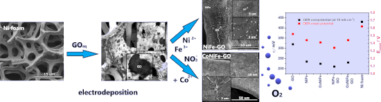
- mainly on chemically synthesized catalysts, which usually required post-processing and some additives (e.g. Nafion) to form an ink to produce an OER electrode. This, in turn, significantly affects the final structure and electrocatalytic performance of the electrode. Therefore, in this work, the


A super-oscillatory step-zoom metalens for visible light
Beilstein J. Nanotechnol. 2022, 13, 1220–1227, doi:10.3762/bjnano.13.101

- high optical loss and are not suitable for far-field imaging. As a result, it is still a huge challenge to achieve unlabeled far-field imaging without image post processing. Optical super-oscillation is a unique optical phenomenon in which an optical signal can oscillate faster locally than its maximum


Reliable fabrication of transparent conducting films by cascade centrifugation and Langmuir–Blodgett deposition of electrochemically exfoliated graphene
Beilstein J. Nanotechnol. 2022, 13, 666–674, doi:10.3762/bjnano.13.58

- processes can be produced from inexpensive and widely available centrifugal post-processing of existing commercially available solutions of electrochemically exfoliated graphene. The demonstrated methodology will lower the entry barriers for new research and industrial uses, since it allows researchers with
- size selection is the route to take towards the mass use of 2D materials in solution. Although size selection through post-processing with cascade centrifugation has been demonstrated in the context of ultrasonic LPE materials [30][31], to the best of our knowledge, the method has not been applied to


Investigation of electron-induced cross-linking of self-assembled monolayers by scanning tunneling microscopy
Beilstein J. Nanotechnol. 2022, 13, 462–471, doi:10.3762/bjnano.13.39

- the white square). (c) Height profiles along lines 1 and 2 marked in Figure 4b. The measured depth is ≈0.1 nm. (d) High-magnification STM image of the monolayer irradiated at a dose of 25 mC/cm2. The voids are preferentially located in darker regions of the monolayer. This image was generated by post
- -processing of Supporting Information File 1, Figure S8a using the continuous wavelet transform function. (e) A high magnification view of the marked area in Figure 4d highlights the remainders of the ordered layer. (f) Top panel: lateral distribution of the voids. The fit (red dashed curve) follows a Poisson


A non-enzymatic electrochemical hydrogen peroxide sensor based on copper oxide nanostructures
Beilstein J. Nanotechnol. 2022, 13, 424–436, doi:10.3762/bjnano.13.35

- ) shows the surface morphology of a thermally obtained copper oxide film. The resulting film is a homogeneous, polycrystalline oxide layer consisting of grains of arbitrary shape. In practice, this layer exhibits poor adhesion to the surface and can be easily damaged mechanically during post-processing
- . Figure 1c–f shows the morphology of the copper oxide layer obtained by chemical hydrothermal oxidation. The resulting coating is characterized by a high degree of uniformity, good adhesion to the copper surface and stability during post-processing. The resulting coating consists of a dense uniform layer


Theoretical understanding of electronic and mechanical properties of 1T′ transition metal dichalcogenide crystals
Beilstein J. Nanotechnol. 2022, 13, 160–171, doi:10.3762/bjnano.13.11

- fitting a second-order polynomial to the change on the total energy versus applied strain. The data are obtained from post-processing the VASP calculated results using the VASPKIT code [45]. The average values of G and B of bulk TMDs are obtained using the Voigt–Reuss–Hill average method [16]: The values


Sputtering onto liquids: a critical review
Beilstein J. Nanotechnol. 2022, 13, 10–53, doi:10.3762/bjnano.13.2


Two dynamic modes to streamline challenging atomic force microscopy measurements
Beilstein J. Nanotechnol. 2021, 12, 1226–1236, doi:10.3762/bjnano.12.90

- lines during subsequent image processing. In some cases, such as when high protrusions are adjacent to flat areas, this fitting will give poor results. Using VM yields high-quality raw images that do not require post-processing. Figure 2e and Figure S2 in Supporting Information File 1 illustrate this


Irradiation-driven molecular dynamics simulation of the FEBID process for Pt(PF3)4
Beilstein J. Nanotechnol. 2021, 12, 1151–1172, doi:10.3762/bjnano.12.86

- multi-parameter problem. Indeed, different precursor molecules, substrate types, irradiation, replenishment and post-processing regimes, and additional molecular species that may facilitate precursor decomposition can be explored to improve the purity of grown deposits and increase the deposition rate


