Search results
Search for "scanning electron microscopy" in Full Text gives 666 result(s) in Beilstein Journal of Nanotechnology. Showing first 200.
Spatial mapping of photovoltage and light-induced displacement of on-chip coupled piezo/photodiodes by Kelvin probe force microscopy under modulated illumination
Beilstein J. Nanotechnol. 2023, 14, 1059–1067, doi:10.3762/bjnano.14.87

- -sectional scanning electron microscopy images can be found in [32]. The top view of the piezo/photodiode device is given in Figure 1a, where the inset represents the cross section of the device stack. Owing to the integration of PZT with silicon processing and operation at low voltages, this device can be


Experimental investigation of usage of POE lubricants with Al2O3, graphene or CNT nanoparticles in a refrigeration compressor
Beilstein J. Nanotechnol. 2023, 14, 1041–1058, doi:10.3762/bjnano.14.86

- nanoparticles is presented separately in the subsequent sections to verify the catalog information provided by the manufacturer. In the characterization of the nanoparticles used in the study, field-emission scanning electron microscopy (FE-SEM), energy-dispersive X-ray spectroscopy (EDS), and X-ray diffraction


A visible-light photodetector based on heterojunctions between CuO nanoparticles and ZnO nanorods
Beilstein J. Nanotechnol. 2023, 14, 1018–1027, doi:10.3762/bjnano.14.84

- and paves the way for developing more stable and effective visible-light photodetectors with remarkable photoresponse and shorter rise and decay times. Results and Discussion The morphologies of pure ZnO NRs and CuO NPs/ZnO NRs were examined via scanning electron microscopy (Figure 1). The field
- -emission scanning electron microscopy (FESEM) image of ZnO NRs exhibits nanorods with hexagonal cross section, well aligned with the glass substrate (Figure 1a). Figure 1b indicates that many spherical nanoparticles are formed on the ZnO NRs after spraying the CuO NP solution with a concentration of 0.05 M
- composition of the materials. The morphology of pure CuO NPs and CuO NPs/ZnO NRs was examined by field-emission scanning electron microscopy. UV–vis absorption spectroscopy showed the optical properties of the materials. The photodetector performance was studied through the current–voltage (I–V


Upscaling the urea method synthesis of CoAl layered double hydroxides
Beilstein J. Nanotechnol. 2023, 14, 927–938, doi:10.3762/bjnano.14.76

- CoAl-based LDH synthesis through an ARR method had been demonstrated, morphological aspects were addressed by means of scanning electron microscopy (SEM), transmission electron microscopy (TEM), and atomic force microscopy (AFM) (Figure 4 and Figure 5). For reference x1, well-defined hexagonal single
- electron microscopy (SEM) Scanning electron microscopy data was acquired using a Hitachi S-4800, with a beam energy of 5 keV. The samples on silicon wafers were directly investigated without any surface coating. Energy dispersive X-ray (EDS) spectroscopy studies were performed on a Hitachi S-4800
- spin-coated on a Si wafer (3000 rpm, 40 s), washed with ethanol and dried afterward. For AFM, the samples were diluted in ethanol and drop-cast on a Si/SiO2 wafer. Si/SiO2 wafers were washed by spin-coating ten droplets of acetone and ten droplets of isopropanol prior to sample deposition. Scanning


Green SPIONs as a novel highly selective treatment for leishmaniasis: an in vitro study against Leishmania amazonensis intracellular amastigotes
Beilstein J. Nanotechnol. 2023, 14, 893–903, doi:10.3762/bjnano.14.73

- , scanning electron microscopy and chemical element mapping analysis were carried out to confirm the uptake of the SPIONs by L. amazonensis intracellular amastigotes after removing the plasma membrane to expose the cytoplasmic environment (Figure 2). Secondary electron imaging revealed intracellular
- . It is the first time that superparamagnetic iron oxide nanoparticles SPIONs are observed inside the Leishmania spp and the parasitophorous vacuole. Chemical element mapping analysis by scanning electron microscopy confirmed the ferrous nature of the nanoparticle aggregates. These results prove the
- PBS pH 7.2, fixed, and post-fixed according to previously published protocols [23]. Then, cells were processed for scanning electron microscopy and chemical element mapping analysis as described in [9]. The micrographs were obtained using a TESCAN VEGA 3 LMU scanning electron microscope operating at


Industrial perspectives for personalized microneedles
Beilstein J. Nanotechnol. 2023, 14, 857–864, doi:10.3762/bjnano.14.70

- with varying heights were printed via two-photon polymerization on a “Quantum X shape” lithography system, and the 10 × 10 microneedle array was printed in 130 min. The scale bar is 1 mm in both images. (A) Scanning electron microscopy image of microcones. (B) Optical microscopy image of transparent
- microcones. Various solid and hollow microneedle designs printed via two-photon polymerization on a “Quantum X shape” lithography system. (A) Scanning electron microscopy image of a 4 × 4 array consisting of both solid and hollow microneedles. The designs were inspired by Mizuno et al. [32] and Cordeiro et


Biomimetics on the micro- and nanoscale – The 25th anniversary of the lotus effect
Beilstein J. Nanotechnol. 2023, 14, 850–856, doi:10.3762/bjnano.14.69

- epicuticular wax coverage on leaves of Deschampsia antarctica as a possible adaptation to severe environmental conditions”, used cryo-scanning electron microscopy to study surfaces of D. antarctica, one of the only two flowering plants native to Antarctica. The results show that the two-layered wax, which
- were performed and the mandibles were analysed using (cryo-) scanning electron microscopy, indicating that a fluid substance covers the medial surface of the mandibles reducing propolis adhesion. Weiser et al. [13] take biomimetics into industrial production with their paper “Roll-to-roll fabrication
- Mail, Kerstin Koch, Thomas Speck, William M. Megill and Stanislav N. Gorb Eggenstein-Leopoldshafen, Kleve, Freiburg, and Kiel, July 2023 Biological archetype and eponym of the lotus effect: The sacred lotus (Nelumbo nucifera). a) Photo of a lotus plant. b) Scanning electron microscopy (SEM) image of


Ultralow-energy amorphization of contaminated silicon samples investigated by molecular dynamics
Beilstein J. Nanotechnol. 2023, 14, 834–849, doi:10.3762/bjnano.14.68

- substantially more controllable at low energies [10][11], which also makes such beams valid candidates for these processes. Another application includes lamella preparation for transmission electron microscopy (TEM). TEM and scanning electron microscopy (SEM) have high constraints regarding cleanliness [12


A wearable nanoscale heart sound sensor based on P(VDF-TrFE)/ZnO/GR and its application in cardiac disease detection
Beilstein J. Nanotechnol. 2023, 14, 819–833, doi:10.3762/bjnano.14.67

- . Composition and β-phase content of the piezoelectric composite films were analyzed using X-ray diffraction. The morphology of the composite film fibers was observed through scanning electron microscopy. Finally, the P(VDF-TrFE)/ZnO/graphene composite film was encapsulated in a sandwich-structure heart sound
- utilized to analyze the composition and β-phase content of the composite piezoelectric nanofilms, while scanning electron microscopy (SEM) was employed to observe the morphology of the thin film filaments. Figure 6 displays the XRD patterns of the three composite piezoelectric nanofilms. In the P(VDF-TrFE


In situ magnesiothermic reduction synthesis of a Ge@C composite for high-performance lithium-ion batterie anodes
Beilstein J. Nanotechnol. 2023, 14, 751–761, doi:10.3762/bjnano.14.62

- carried out for structural and phase information. Infrared (IR, Shimadzu IRAffinity-1S) and Raman (LabRAM HR evolution confocal Raman microscope) spectra were measured for bond analysis. Field-emission scanning electron microscopy (FE-SEM, Hitachi S-4800) and high-resolution transmission electron


Control of morphology and crystallinity of CNTs in flame synthesis with one-dimensional reaction zone
Beilstein J. Nanotechnol. 2023, 14, 741–750, doi:10.3762/bjnano.14.61

- by field-emission scanning electron microscopy (FESEM, Zeiss Crossbeam 340) coupled with energy-dispersive X-ray analysis (EDX) for morphology and elemental analysis. Raman spectroscopy (HORIBA XploRA PLUS, 532 nm) was done to analyze the signature spectra of the grown CNTs. Line-of-sight images of


Humidity-dependent electrical performance of CuO nanowire networks studied by electrochemical impedance spectroscopy
Beilstein J. Nanotechnol. 2023, 14, 683–691, doi:10.3762/bjnano.14.54

- cell geometry and a parallel circuit scheme. Scanning electron microscopy: (a) CuO nanowires grown on Cu substrate by thermal oxidation; (b) system of Cr/Au microelectrodes with teeth-like shape; (c–f) pairs of microelectrodes (c, e) without and (d, f) with dielectrophoretically aligned nanowires
- electron microscopy (SEM, Hitachi S4800) and atomic force microscopy (AFM, Asylum Research MFP-3D). Electrochemical impedance measurements were performed under various atmospheric conditions in a custom-made system described elsewhere [28]. The main system parameters were RH from 4% to 97%, gas flow from
- in 10 × 10 mm2 chips. To assemble the nanowires by dielectrophoresis, the chip was submerged in a suspension of the nanowires in IPA, and an AC voltage (5 V peak to peak, 5–50 kHz) was applied between the microelectrodes for 20 min [26]. Nanowires and microelectrodes were examined by scanning


SERS performance of GaN/Ag substrates fabricated by Ag coating of GaN platforms
Beilstein J. Nanotechnol. 2023, 14, 552–564, doi:10.3762/bjnano.14.46

- substrates were examined regarding their optical properties using UV–vis spectroscopy and regarding their morphology using scanning electron microscopy. SERS properties of the fabricated GaN/Ag substrates were evaluated by measuring SERS spectra of 4-mercaptobenzoic acid molecules adsorbed on them. For all
- morphology of fabricated Ag layers examined by scanning electron microscopy (SEM). Then, we present the results of their optical properties determined using UV–vis spectroscopy. Finally, we compare the SERS performance of the GaN/Ag substrates toward 4-mercaptobenzoic acid (pMBA) molecules adsorbed on them


Observation of multiple bulk bound states in the continuum modes in a photonic crystal cavity
Beilstein J. Nanotechnol. 2023, 14, 544–551, doi:10.3762/bjnano.14.45

- carried out to compensate for deviations between fabricated and designed values. To obtain devices with larger Q factors and higher scattering power, cavities with larger Na = 30 and Nb = 10 were fabricated. Optical and scanning electron microscopy (SEM) images are given in Figure 3a. A microscope was
- all bulk modes. (d) The near-field H field intensity distribution of modes M11 to M44. The yellow dashed squares indicate the boundary of region A. Fabricated samples and optical setup. (a) Optical and scanning electron microscopy images of fabricated samples, scale bar: 10 μm. (b) Diagram of the


Carbon nanotube-cellulose ink for rapid solvent identification
Beilstein J. Nanotechnol. 2023, 14, 535–543, doi:10.3762/bjnano.14.44

- length of 5 μm were produced at CTNano/UFMG [59][60][61]. Morphological analysis was carried out by scanning electron microscopy (SEM) in a Quanta 200 FEG, using secondary electrons between 2 and 10 kV. Atomic force microscopy (AFM) was carried out on a Bruker MultiMode8 SPM using the intermittent


On the use of Raman spectroscopy to characterize mass-produced graphene nanoplatelets
Beilstein J. Nanotechnol. 2023, 14, 509–521, doi:10.3762/bjnano.14.42

- widely used characterization tool for GR2Ms [8]. A search of Web of Science showed that of 97,532 articles published in the last five years with “Graphene” in the abstract, 9.3% also mentioned “Raman”. This is compared with atomic force microscopy (AFM) (2.4%), scanning electron microscopy (SEM) (11.4


The origin of black and white coloration of the Asian tiger mosquito Aedes albopictus (Diptera: Culicidae)
Beilstein J. Nanotechnol. 2023, 14, 496–508, doi:10.3762/bjnano.14.41

- analysed using scanning electron microscopy, transmission electron microscopy, and fluorescence microscopy. Reflectance spectra of the white areas are measured. No clear difference is present in the morphology of micro- and nanostructures of black and white scales in SEM and TEM, but black scales contain a
- . The ultrastructure of the white and black scales on the hindlegs of Ae. albopictus is analysed using scanning electron microscopy, transmission electron microscopy, and fluorescence microscopy. Moreover, reflectance spectra of the white areas are measured. The scales are present also on other body
- , and with an excitation filter 546 nm, chromatic beam splitter FT 580 nm, emission 590 nm. Insect legs were removed from the insects and placed on a microscope slide for observations. Scanning electron microscopy and cryo-SEM Dry insects were observed in a scanning electron microscope Hitachi S-4800


Mixed oxides with corundum-type structure obtained from recycling can seals as paint pigments: color stability
Beilstein J. Nanotechnol. 2023, 14, 467–477, doi:10.3762/bjnano.14.37

- results. The Raman modes are A1g (ca. 149 cm−1 and ca. 501 cm−1) and E1g (ca. 222 cm−1, ca. 290 cm−1, ca. 298 cm−1, ca. 402 cm−1, and ca. 615 cm−1, where 290 cm−1 and 298 cm−1 usually are a doublet with E1g symmetry and cannot be easily resolved [20]. Scanning electron microscopy (SEM) The morphology of
- the four vibrational modes E1g characteristic of Cr2O3, and (b) sample 2, which features the seven characteristic vibrational modes (two A1g modes and five E1g modes) of Fe2O3. Scanning electron microscopy images of (a) sample 1 (low magnification, SE detector), (b) sample 1 (high magnification, SE


Evaluation of electrosynthesized reduced graphene oxide–Ni/Fe/Co-based (oxy)hydroxide catalysts towards the oxygen evolution reaction
Beilstein J. Nanotechnol. 2023, 14, 420–433, doi:10.3762/bjnano.14.34
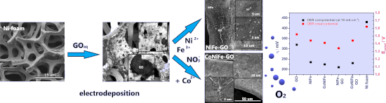
- the electrodeposition of conductive films on active metals [26]. The morphology of the deposits was analyzed by scanning electron microscopy (SEM) and is presented in Figure 1b–f. Typical GO flakes regularly distributed over the surface of the nickel foam were successfully obtained after the one-step


Biocatalytic synthesis and ordered self-assembly of silica nanoparticles via a silica-binding peptide
Beilstein J. Nanotechnol. 2023, 14, 280–290, doi:10.3762/bjnano.14.25

- scattering (DLS). The efficiency of the self-assembly was evaluated with scanning electron microscopy (SEM), UV–vis spectroscopy, and qualitative visual demonstration. Results and Discussion SiBP alone as catalyst Reaction kinetics were studied via OD measurements of the particles and GC analysis of
- covers were moved completely out of the colloidal solution. Scanning electron microscopy To analyze as-synthesized particles, 50 µL aliquots of the reaction solutions were placed on standard microscope cover slides. The excess liquid was removed by absorbing on a clean absorbent paper. To analyze self


Batch preparation of nanofibers containing nanoparticles by an electrospinning device with multiple air inlets
Beilstein J. Nanotechnol. 2023, 14, 141–150, doi:10.3762/bjnano.14.15

- using an electronic balance (XJ120A, Precisa LTD.). The nanofiber morphology was investigated by a scanning electron microscopy (SEM, Hitachi S4800, Hitachi LTD.), and Image J software (National Institute of Mental Health) was used to characterize the fiber diameter distribution by random selection of


Formation of nanoflowers: Au and Ni silicide cores surrounded by SiOx branches
Beilstein J. Nanotechnol. 2023, 14, 133–140, doi:10.3762/bjnano.14.14

- annealed at 1050 °C was named 15Au5Ni. The morphology was imaged by optical microscopy (OM, Zeiss Axiotech) and high-resolution scanning electron microscopy (HR-SEM, Hitachi S-4800) equipped with energy-dispersive X-ray spectroscopy (EDS, Thermo Scientific). The SEM images were recorded by using mixed


Antimicrobial and mechanical properties of functionalized textile by nanoarchitectured photoinduced Ag@polymer coating
Beilstein J. Nanotechnol. 2023, 14, 95–109, doi:10.3762/bjnano.14.11

- , as well as the final thickness of the metallic layer, account for this difference in reflectivity. Scanning electron microscopy (SEM) carried out on the surface of functionalized textiles revealed the homogenous distribution of AgNPs, with average sizes of 62 ± 2 nm and 58 ± 1 nm for the Ag@PEG600DA
- electron microscopy (SEM), transmission electron microscopy (TEM), and reflectance measurements to assess the optical properties and the durability of the functionalized textiles. Results and Discussion Photoinduced synthesis of the Ag@polymer coating Specific monomers poly(ethylene glycol) 600 diacrylate
- measurements. A Bio photometer UV–vis spectrometer from Eppendorf was used to assess bacteria and yeast suspensions by OD measurements at 600 nm. Surface characterizations were carried out using transmission electron microscopy (TEM) at 200 kV on a Philips CM200 instrument (LaB6 cathode) and scanning electron


Combining physical vapor deposition structuration with dealloying for the creation of a highly efficient SERS platform
Beilstein J. Nanotechnol. 2023, 14, 83–94, doi:10.3762/bjnano.14.10

- SERS properties of the nanoporous structure. Using scanning electron microscopy (SEM) and X-ray photoelectron spectroscopy (XPS) the morphology and surface composition of each nanoporous structure were respectively evaluated and used to describe the SERS properties of the samples. Results and
- 20 min to stop the dealloying process and to ensure a good cleaning of the samples. Characterization Scanning electron microscopy micrographs were recorded using a HITACHI STEM-FEG with an acceleration voltage of 5 kV. The images were treated with the ImageJ software [58] to assess the size of the


Induced electric conductivity in organic polymers
Beilstein J. Nanotechnol. 2022, 13, 1551–1557, doi:10.3762/bjnano.13.128

- polymer film thickness, which is just 3 nm. After electric measurements, a number of heterostructures was sent for analysis by high resolution transmission electron microscopy and/or scanning electron microscopy. None of the studied samples showed a systematic ‘sticking’ of lead electrodes through the


