Search results
Search for "transmittance" in Full Text gives 112 result(s) in Beilstein Journal of Nanotechnology.
High permittivity, breakdown strength, and energy storage density of polythiophene-encapsulated BaTiO3 nanoparticles
Beilstein J. Nanotechnol. 2020, 11, 1190–1197, doi:10.3762/bjnano.11.103

- −1 [15][16]. The broad transmittance peak at 3418 cm−1 and weak bands in the range of 2845–2935 cm−1 are attributed to the adsorbed water molecules (νO–H) and the carbonaceous impurities (νCH3, νCH2) in PTh, respectively. A peak at 1123 cm−1 that is also characteristic of PTh corresponds to the Cα–Cα
- resonance absorption between two thiophene rings [17]. It demonstrates that PTh is predominantly formed by Cα–Cα conjunction during the low-temperature oxidative polymerization. The transmittance peaks at 1035 cm−1 and 788 cm−1 further prove this point as they indicate the out-of-plane bending (τCβ–H) and


Highly sensitive detection of estradiol by a SERS sensor based on TiO2 covered with gold nanoparticles
Beilstein J. Nanotechnol. 2020, 11, 1026–1035, doi:10.3762/bjnano.11.87

- TiO2 porosity. Optical properties Figure 4 reports the optical transmittance of the TiO2/Au samples. Our previous studies involving TiO2/Au systems have shown that the reflectance has low values of about 5% and can thus be considered negligible [28]. A general decrease of the optical transmittance was
- observed for large quantities of Au and the transmittance was influenced by the growth conditions and the thermal treatment. For example, in the case of 6 nm of Au the wavelength at which maximum absorption occurs changed after annealing from about 620 to 560 nm (Table 2). These trends were outlined also


Effect of Ag loading position on the photocatalytic performance of TiO2 nanocolumn arrays
Beilstein J. Nanotechnol. 2020, 11, 717–728, doi:10.3762/bjnano.11.59

- concentration promotes the generation of active radicals, which increases the catalytic reaction rate and the catalytic efficiency [41][43]. In Figure 9b and 9d, a schematic diagram of the energy conversion of the two different nanocolumn structures is shown. In the AFT structure, the good transmittance of TiO2


Structural optical and electrical properties of a transparent conductive ITO/Al–Ag/ITO multilayer contact
Beilstein J. Nanotechnol. 2020, 11, 695–702, doi:10.3762/bjnano.11.57

- transmittance (86.1%) with a very low sheet resistance of 2.93 Ω/sq. The carrier concentration increased more than twice when the Al–Ag layer was inserted between the ITO layers. The figure of merit of the IAAI multilayer contact has been found to be high at 76.4 × 10⁻³ Ω−1 compared to a pure ITO contact (69.4
- smaller thickness would result in high optical transmittance in the visible region. However, the resistivity would increase, which is an issue [4][7][8]. Therefore, the search for new material compositions and structures of ITO-based films to enhance the performance in optoelectronic devices is of
- indium metal is needed [9][10][11]. The insertion of a metal layer reduces the transparency of the ITO electrode due to opaqueness of the metal, but selecting an optimal metal thickness can effectively decrease the reflection from the metal film and thus enhance the transmittance. Furthermore, it gives


Recent progress in perovskite solar cells: the perovskite layer
Beilstein J. Nanotechnol. 2020, 11, 51–60, doi:10.3762/bjnano.11.5

- to convert it into the proper perovskite phase, which is termed the “half step”. Efficient semi-transparent PSCs with a PCE of 10.03% and an average visible transmittance (AVT) of 28% were achieved. The devices prepared by the 1.5-step process show better performance than those prepared by the one


Gold and silver dichroic nanocomposite in the quest for 3D printing the Lycurgus cup
Beilstein J. Nanotechnol. 2020, 11, 16–23, doi:10.3762/bjnano.11.2

- Lycurgus cup might be possible by studying the reflectance and transmittance spectra from the Lycurgus cup and matching them with freshly synthesised Au and Ag nanoparticles in PVA. However, such spectra are missing in literature and the only few present are hand-drawn [13], making it impossible to


Plasmonic nanosensor based on multiple independently tunable Fano resonances
Beilstein J. Nanotechnol. 2019, 10, 2527–2537, doi:10.3762/bjnano.10.243

- and output power flows of the input port1 and output port2, respectively. The transmittance is defined as T = Pout/Pin. Since the width of the bus waveguide is much smaller than the wavelength of the incident light, only a single propagation mode TM0 can exist in the structure, of which the dispersion
- field amplitudes in each part of the waveguide (i = 1, 2) for outgoing (−) or incoming (+) from the resonator. In this paper, only port1 has TM wave incidence. The input and output port are symmetrical with the same w about the resonance system. Hence, S2+ = 0, τn1 = τn2 = τn, and the transmittance T is
- element method (FEM), which is also comparative to MICMT. The transmittance values are calculated according to the definition of Equation 8. It is well known that the excitation of Fano resonance requires the interaction of continuous (bright) modes and discrete (dark) modes. In our design, stub1 can form


Multiple Fano resonances with flexible tunablity based on symmetry-breaking resonators
Beilstein J. Nanotechnol. 2019, 10, 2459–2467, doi:10.3762/bjnano.10.236

- angle is ϕ = 0° and the deviation distance is d = 0. Figure 2 shows the transmission spectra of the designed waveguide–resonator coupled system. Different values of the thickness of the metal wall, t, were studied. When a metal wall is placed in a MDM waveguide, the transmittance is low over a wide


Semitransparent Sb2S3 thin film solar cells by ultrasonic spray pyrolysis for use in solar windows
Beilstein J. Nanotechnol. 2019, 10, 2396–2409, doi:10.3762/bjnano.10.230

- Sb2S3 thin films and transmittance of solar cells without P3HT/Au back contact. The AVT of the stacks of glass/ITO/TiO2/Sb2S3 with 70, 100, and 150 nm of Sb2S3 is 28%, 26%, and 16%, respectively in the 380–740 nm wavelength range (Figure 3b). Thus, the 150 nm thick Sb2S3 film is already too opaque for
- absorption coefficient curves of Sb2S3 and P3HT. The transmittance of light to the absorber is limited at higher photon energies by the onset of absorption of TiO2 at 3.0 eV and ITO at 3.6 eV. The P3HT layer, however, does not contribute to the generation of photocurrent [14][21]. On the contrary, any
- 600, FEI Company). The optical properties were measured using a UV–vis–NIR spectrophotometer (Jasco V-670, integrating sphere, air reference). The AVT was calculated as the arithmetic average of total transmittance of the glass/ITO/TiO2/Sb2S3 stack in the 380–740 nm wavelength range by using Equation


Design of a nanostructured mucoadhesive system containing curcumin for buccal application: from physicochemical to biological aspects
Beilstein J. Nanotechnol. 2019, 10, 2304–2328, doi:10.3762/bjnano.10.222


Nonlinear absorption and scattering of a single plasmonic nanostructure characterized by x-scan technique
Beilstein J. Nanotechnol. 2019, 10, 2182–2191, doi:10.3762/bjnano.10.211

- experimental feasibility and the capability to determine both the nonlinear refractive index and the nonlinear absorption [21]. Below, we briefly address the principle of z-scan and its limitations. The z-scan technique is based on measurement of transmittance as a thin sample moves along the propagation path
- large-area power detector. If there is no nonlinearity, the transmittance will be constant no matter where the sample is. However, when there is nonlinear absorption, the transmittance changes as the sample is in the vicinity of the focus, where the intensity is highest along the beam path. Therefore
- , the open-aperture setup is sensitive to nonlinear absorption and measures the imaginary part of the nonlinear refractive index. In the closed-aperture setup, the transmittance is measured through a small aperture in front of the power detector, so the detected signal is sensitive to beam divergence


Biocatalytic oligomerization-induced self-assembly of crystalline cellulose oligomers into nanoribbon networks assisted by organic solvents
Beilstein J. Nanotechnol. 2019, 10, 1778–1788, doi:10.3762/bjnano.10.173

- equation: where Icor is the corrected intensity, Iobs is the observed intensity, t is the X-ray transmittance through the sample, and Iblank is the intensity measured without any sample. The amorphous cellulose halo obtained previously [42] was fitted to the 1D profiles in 2θ ranges adequately selected


Revisiting semicontinuous silver films as surface-enhanced Raman spectroscopy substrates
Beilstein J. Nanotechnol. 2019, 10, 1048–1055, doi:10.3762/bjnano.10.105

- ][48][49][50][51][52][53][54][55]. However, transmittance, reflectance and absorption are rarely reported in these studies, and it is difficult to link the optical properties of these nanostructures with their SERS performance. In our earlier initial study we investigated SSFs as SERS substrates [55
- quartz crystal microbalance. Characterization of semicontinuous silver films Optical properties of SSFs were characterized using UV–vis–NIR Perkin Elmer Lambda 900 spectrometer. Transmittance was measured using a standard detector, while reflectance was measured with an integrating sphere module
- . Absorption was calculated assuming the sum of transmittance, reflectance, and absorption is 100%. The morphology of the fabricated structures was measured using a Quanta 3D FEG Dual Beam scanning electron microscope (SEM) and an atomic force microscope (AFM). The SEM images of SSFs were converted to black


Nanoscale optical and structural characterisation of silk
Beilstein J. Nanotechnol. 2019, 10, 922–929, doi:10.3762/bjnano.10.93

- polarisation at the IR spectral range of λ = 750–4000 cm−1 (2.5–13.3 μm); the extinction of polarisers was Tmax/Tmin ≈ 150 and the transmittance was about 50%. The far-field transmission measurements were carried out with a 36× magnification Cassegrain objective lens (NA = 0.5) at the corresponding resolution
- of 0.61λ/NA ≈ 4.1 μm at the 3000 cm−1 band (λ = 3.33 μm). The absorbance or optical density A = −log(T) spectrum is defined by the absorption coefficient α ≡ 4πκ/λ = 2ωκ/c [cm−1] for the transmitted light intensity IT = I0e−αd = I0 × 10−OD; where d is the thickness of sample, the transmittance T = IT


Rapid, ultraviolet-induced, reversibly switchable wettability of superhydrophobic/superhydrophilic surfaces
Beilstein J. Nanotechnol. 2019, 10, 866–873, doi:10.3762/bjnano.10.87

- –CF3 groups) undergo no obvious changes either under UV illumination or high temperature exposure. The change in transmittance for selected transitions are listed in Figure 3b, which shows that the change of –OH in TiO2 is much larger than the change of –CF2- or –CF3 in PFOS. The change of –CF2- or
- locations. SEM images of TiO2–PFOS and Al2O3–PFOS composite surfaces. FTIR spectra of TiO2 and TiO2–PFOS, Al2O3 and Al2O3–PFOS. (a) Contact angle and FTIR spectrum of the TiO2–PFOS surface under different treatment conditions. (b) The change in transmittance for selected transitions, –OH, –CF2- and –CF3. (a
- ) Contact angle and FTIR spectrum of the Al2O3–PFOS surface under different treatment conditions. (b) The change in transmittance for selected transitions, –OH, –CF2- and –CF3. The possible mechanism describing the transition of TiO2 and PFOS under UV illumination and heating. Reversible superhydrophobic


Outstanding chain-extension effect and high UV resistance of polybutylene succinate containing amino-acid-modified layered double hydroxides
Beilstein J. Nanotechnol. 2019, 10, 684–695, doi:10.3762/bjnano.10.68

- UV radiation of the polymer chains. UV–vis transmittance spectra of PBS and the nanocomposites with 5 wt % of Mg2Al LDHs are presented in Figure 10. The largest decrease in transmittance is observed for PBS–LDH/PHE, then for PBS–LDH/HIS. As mentioned for the hybrid LDH materials, the absorption band
- can be caused by the cycle phenyl or imidazole acting as a chromophore. Also, PBS with Mg2Al/nitrate LDH shows lower transmittance, as described above. The evolution of the UV–vis transmittance of PBS and PBS nanocomposites was measured during photodegradation at 60 °C (Supporting Information File 1
- , Figure S5). The transmittance spectra for PBS are not modified during the entire period of irradiation. In the case of PBS nanocomposites with LDH/nitrate and LDH/HIS, the transmittance decreases during the first 20 h and then stabilizes. When the PBS nanocomposite with LDH/PHE is irradiated, the


Direct observation of the CVD growth of monolayer MoS2 using in situ optical spectroscopy
Beilstein J. Nanotechnol. 2019, 10, 557–564, doi:10.3762/bjnano.10.57

- substrates has been monitored in situ using differential transmittance spectroscopy (DTS). The growth of the MoS2 monolayer can be precisely followed by observation of the evolution of the characteristic optical features. Consequently, a strong correlation between the growth rate of the MoS2 monolayer and
- the optical properties of 2D TMDCs [2][20] and, most recently, also to monitor the molecular beam epitaxy of monolayer MoSe2 on sapphire substrates [27]. In the current work, we have applied an analogous technology, namely, differential transmittance spectroscopy (DTS), to realize the in situ real
- time study of the CVD growth of monolayer MoS2 on Al2O3(0001) surface. In this case, the normalized difference between the transmittance through the bare substrate and the transmittance after a given deposition time are resolved. By monitoring using DTS during growth, the evolution of the optical


Gold nanoparticles embedded in a polymer as a 3D-printable dichroic nanocomposite material
Beilstein J. Nanotechnol. 2019, 10, 442–447, doi:10.3762/bjnano.10.43

- 4th century puzzled scientists for long time: The Lycurgus cup [7]. This cup has a very peculiar dichroic filter property [8], as its color is dependent on the illumination angle, changing from clear red (transmittance) to opaque green (reflectance). It was later found that this optical property was


Development of an anti-pollution coating process technology for the application of an on-site PV module
Beilstein J. Nanotechnol. 2019, 10, 332–336, doi:10.3762/bjnano.10.32

- annealing treatments were applied to PV module glasses, i.e., furnace, rapid thermal annealing (RTA) and torch. Among these, torch annealing, which can be easily carried out at PV module installation sites, was applied to PV module glasses using different numbers of repetition. Light transmittance, contact
- light transmittance of 95% or higher [5][6]. Large solar power plants are currently being installed for power generation, and a huge amount of time and cost is required for maintenance, including surface cleaning. Therefore, the introduction of a technology capable of easily removing pollutants using
- were measured using the integrating sphere of a UV–visible spectrophotometer (Mega 700, Scinco Co., Ltd., South Korea). Results and Discussion The light transmittance measurement results of the fabricated functional coatings are summarized in Figure 1. The light transmittance of the coating film


Magnetic-field sensor with self-reference characteristic based on a magnetic fluid and independent plasmonic dual resonances
Beilstein J. Nanotechnol. 2019, 10, 247–255, doi:10.3762/bjnano.10.23
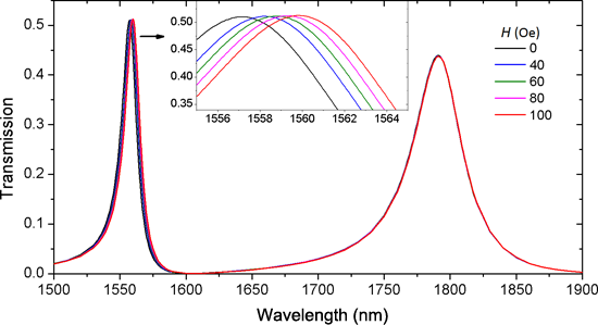
- waveguide structures are plotted in Figure 2. It is seen that for the individual resonator, there is a wavelength range in which the transmittance is low, as shown by the green and blue lines. For the stub–disk coupled waveguide structure, a transmission peak appears in the transmission dip, as shown by the
- theoretical analysis. When a disk is coupled to the upper stub 1, cavities modes can directly couple with each other through their evanescent field at small gap distances. When ω1 = ωd = ω, the transmittance of Equation 8 becomes T = |(κ1d + 1)/(κw1 + κ1d + 1)|2. This indicates that a transmission peak


Uniform Sb2S3 optical coatings by chemical spray method
Beilstein J. Nanotechnol. 2019, 10, 198–210, doi:10.3762/bjnano.10.18

- thickness of 100 nm derived from SEM images (Table 3). The absorption coefficient α was determined as where d is the layer thickness, R is the total reflectance, included to compensate for thin film interference, and T is the total transmittance. The band gap of Sb2S3 layers was determined by plotting (αhν
- 0.02°, 5°/min, silicon strip detector D/teX Ultra). The crystal structure and phase composition were analyzed using Rigaku PDXL 2 software. Optical total transmittance and total reflectance spectra of glass/ITO/TiO2 reference and glass/ITO/TiO2/Sb2S3 samples were measured in the 250–1600 nm range vs
- optical transmittance spectra of glass/ITO/TiO2/Sb2S3 samples. Supporting Information Supporting Information File 34: Additional XRD, EDX data, SEM images, Lorentzian fitting of Sb2S3 Raman vibrational bands, and Tauc plots. Acknowledgements We acknowledge Dr. Valdek Mikli from the Laboratory of


Co-intercalated layered double hydroxides as thermal and photo-oxidation stabilizers for polypropylene
Beilstein J. Nanotechnol. 2018, 9, 2980–2988, doi:10.3762/bjnano.9.277

- HnMn′-Ca2Al-LDHs. Figure 7b demonstrates the visible-light transmittance of HnMn′-Ca2Al-LDH/PP composite films, which is one of crucial properties of the PP products. All the samples show a similar trend demonstrating that there is a good dispersion of Ca2Al-LDHs in the PP matrix without affecting its
- transmittance spectra of Ca2Al/PP composites. (c) SEM image and (d) Al (left) and Ca (right) element mapping of the H1M1-Ca2Al/PP composite. (a) TGA curves of HnMn′-Ca2Al/PP composites. (b) FTIR spectra of PP after different periods of thermal aging. (c) Thermal aging and (d) photo-oxidation aging of HnMn


Near-infrared light harvesting of upconverting NaYF4:Yb3+/Er3+-based amorphous silicon solar cells investigated by an optical filter
Beilstein J. Nanotechnol. 2018, 9, 2788–2793, doi:10.3762/bjnano.9.260

- the visible range; however, they are almost transparent for near-infrared radiation (NIR, 700–2500 nm), which constitutes 52% of the energy of the entire solar spectrum [2][3]. The transmittance of NIR light is one of the major energy-loss mechanisms for conventional a-Si:H solar cells [4][5]. This
- point (0.45 V, 12.45 mA). The inset shows a photograph with the active area of ca. 0.84 cm2. The external quantum efficiency (EQE) curve in Figure 3c reveals that almost no photocurrent is generated when the wavelength of light is longer than 800 nm. The transmittance spectrum of a-Si:H solar cell
- without back reflector in Figure 3d shows that nearly 50% of the incident light with wavelengths longer than 800 nm passes through the cell. Given the large proportion of transmittance loss in NIR range, the a-Si:H solar cell would benefit much from the incorporation of UC. Under solar irradiation, the


Impact of the anodization time on the photocatalytic activity of TiO2 nanotubes
Beilstein J. Nanotechnol. 2018, 9, 2628–2643, doi:10.3762/bjnano.9.244

- potentiostatic bias of 1 V/Ag|AgCl for a period of 180 min. Simultaneously, the kinetics of the degradation of MB were followed using the transmittance of a 638 nm red laser and the solution measured with a photodiode at fixed distances. The evaluated solution was fed into a quartz cuvette with a peristaltic


Au–Si plasmonic platforms: synthesis, structure and FDTD simulations
Beilstein J. Nanotechnol. 2018, 9, 2599–2608, doi:10.3762/bjnano.9.241

- frequency domain, which in turn gives results of the properties in a wide-range frequency spectrum, e.g., absorbance and transmittance of the sample, which could be directly compared to results from UV–vis measurements. The combination of experimental and computational methods in the design of materials or


