Abstract
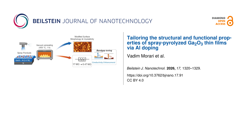
Undoped and Al-doped α-Ga2O3 thin films (1–3 vol % of Al in precursor solution) were successfully deposited on Si substrates by spray pyrolysis at 500 °C and systematically investigated in terms of morphological, structural, compositional, optical, and electrical properties. Atomic force microscopy analysis revealed that moderate Al incorporation significantly improves surface morphology, reducing the root mean square roughness from 2.0 nm (undoped) to a minimum of 1.25 nm at 2 vol % Al, followed by a slight increase at 3 vol % Al due to possible lattice strain and compositional inhomogeneity. Cross-sectional scanning electron microscopy images confirmed the formation of dense, crack-free, and well-adhered films with thicknesses ranging from 445 to 540 nm, indicating that Al incorporation affects growth kinetics. Energy-dispersive X-ray analysis verified successful Al incorporation and slight compositional variations, suggesting modifications in defect chemistry. X-ray diffraction results demonstrated that all films crystallize in the α-Ga2O3 phase with a corundum-type structure, while Al doping significantly influences crystal orientation, crystallite size, and lattice strain without altering the phase. Optical measurements revealed high transparency (≈90%) in the visible region for all samples. The optical bandgap increased slightly from 4.82 eV (undoped) to 4.87 eV (3 vol % Al), indicating successful substitutional incorporation of Al3+ and tunable optical properties. Electrical measurements showed linear current–voltage characteristics, confirming ohmic conduction. The resistance decreased from 17.32 MΩ (undoped) to 0.47 MΩ (3 vol % Al), demonstrating enhanced conductivity while preserving the semiconducting nature of the material. Overall, controlled Al doping effectively tailors the microstructural, optical, and electrical properties of α-Ga2O3 thin films, with 2 vol % Al identified as the optimal concentration for achieving improved surface morphology and balanced functional performance.
Introduction
Gallium oxide (Ga2O3) is an ultrawide-bandgap semiconductor (Eg = 4.5–5.0 eV) [1] that has attracted considerable attention for next-generation power electronics, deep-UV optoelectronics, and high-temperature sensing applications [2-5]. Owing to its large breakdown electric field, high chemical and thermal stability, and optical transparency in the ultraviolet region, Ga2O3 is considered a strong candidate for high-power and high-frequency devices [6]. Among its polymorphs, the β-phase (β-Ga2O3) is the most thermodynamically stable and widely investigated for device applications [7].
The electrical properties of Ga2O3 can be tailored through controlled doping to modify the free carrier concentration and, consequently, the electrical conductivity. n-Type conductivity is commonly achieved by doping with donor elements such as Nb, Sn, Ge or Si, which introduce shallow donor levels near the conduction band [8-11]. The choice of dopant and its concentration strongly influence not only the electrical conductivity but also the structural, optical, and morphological properties of the material. In particular, doping with Al has been explored to tune the bandgap and modify transport properties through the formation of (AlxGa1−x)2O3 solid solutions [12,13]. Controlled Al incorporation also enables effective tuning of structural properties of (AlxGa1−x)2O3 thin films, where moderate doping improves crystalline quality and interface stability, while excessive Al content induces lattice strain and defect accumulation, ultimately influencing the electronic performance of the heterostructure. Al doping has been widely investigated as an effective strategy to modify the structural, optical, and electrical properties of Ga2O3 thin films. Previous studies have demonstrated that the incorporation of Al into the Ga2O3 lattice can influence the carrier concentration, optical bandgap, and defect-related properties, depending on deposition technique and doping level [14]. The incorporation of Al3+ ions into the Ga2O3 lattice is facilitated by the similarity in valence state between Al3+ and Ga3+ ions. However, their ionic radii are different, with Al3+ (approximately 0.535 Å) being smaller than Ga3+ (approximately 0.62 Å) for tetrahedral coordination. This difference facilitates the incorporation of Al ions into the Ga2O3 lattice, on the one hand. However, the partial substitution of Ga3+ by smaller Al3+ ions can induce lattice contraction and local strain within the Ga2O3 structure, on the other hand. Such structural modifications may influence defect formation, particularly oxygen vacancy concentration, which can affect the electrical and optical characteristics of the films [12,14].
Various techniques have been employed for the fabrication of α-Ga2O3 thin films, including sol–gel processing [15], magnetron sputtering [16], chemical vapor deposition (CVD) [17], molecular beam epitaxy (MBE) [18], pulsed laser deposition (PLD) [19], atomic layer deposition (ALD) [20] and spray pyrolysis [21]. Among these, spray pyrolysis is an attractive and cost-effective method due to its simplicity, scalability, and suitability for large-area deposition. The technique allows for good control over film thickness and composition by adjusting parameters such as precursor concentration, substrate temperature, and spray rate [22,23].
Gallium oxide exists in several polymorphic forms, including α-, β-, γ-, δ-, and ε-Ga2O3 phases. Among these, the monoclinic β-Ga2O3 phase is thermodynamically the most stable and has been extensively studied for high-power electronics and ultraviolet optoelectronic devices due to its ultrawide bandgap (≈4.8 eV) and high breakdown field. The metastable α-Ga2O3 phase, which exhibits a corundum-type structure similar to that of α-Al2O3, has attracted increasing attention because of the potential for high-power devices and compatibility with heterostructure engineering. However, the α-phase is thermodynamically less stable and can transform into more stable phases depending on growth conditions and thermal treatment [24].
In the present study, Al-doped α-Ga2O3 thin films (1–3 vol % of Al in precursor solution) were prepared by spray pyrolysis in order to investigate the influence of Al incorporation on the structural and electrical properties. Particular attention was given to the correlation between Al doping level and the resulting changes in crystallinity, microstructure, and electrical conductivity.
Results and Discussion
Surface topography imaging and quantitative surface roughness analysis of the undoped and Al-doped α-Ga2O3 thin films were carried out using atomic force microscopy (AFM) over a scan area of 5 × 5 μm2. The corresponding three-dimensional AFM images are presented in Figure 1. The undoped α-Ga2O3 film exhibits a relatively rough surface with a root mean square (RMS) roughness of 2.0 nm and an average roughness (Ra) of 1.35 nm. The surface consists of densely distributed sharp protrusions, indicating non-uniform grain growth and significant surface irregularities. Upon incorporation of 1 vol % Al, the surface roughness decreases considerably (RMS = 1.42 nm, Ra = 0.92 nm). A further reduction in roughness is observed for the 2 vol % Al-doped α-Ga2O3 film, which exhibits the lowest RMS (1.25 nm) and Ra (0.81 nm) values among all samples. The AFM image reveals a more homogeneous grain distribution with reduced peak density, suggesting improved surface diffusion and enhanced nucleation control during film growth [25]. However, increasing the Al concentration to 3 vol % results in an increase in surface roughness (RMS = 1.81 nm, Ra = 1.09 nm). The surface morphology shows the reappearance of larger protrusions, indicating that excessive Al incorporation may introduce lattice strain, defect formation, or compositional inhomogeneity. This deterioration in surface smoothness at higher doping concentration may be attributed to clustering effects, which disturb the growth kinetics.
![[2190-4286-17-91-1]](/bjnano/content/figures/2190-4286-17-91-1.png?scale=2.0&max-width=1024&background=FFFFFF)
Figure 1: AFM topography (5 × 5 µm2) of undoped and Al-doped α-Ga2O3 films as follows: 0 vol % (a), 1 vol % (b), 2 vol % (c), and 3 vol % (d).
Figure 1: AFM topography (5 × 5 µm2) of undoped and Al-doped α-Ga2O3 films as follows: 0 vol % (a), 1 vol % (...
Overall, the roughness trend follows the relationship
![[2190-4286-17-91-i1]](/bjnano/content/inline/2190-4286-17-91-i1.svg?max-width=590&scale=1.18182)
These results indicate that moderate Al doping (2 vol %) optimizes the surface morphology, producing smoother and more uniform films. Such reduced surface roughness is advantageous for optoelectronic and electronic device applications, as it minimizes interface scattering, improves contact formation, and enhances overall device performance. The extracted roughness parameters are summarized in Table 1.
Cross-sectional SEM micrographs of the undoped and Al-doped α-Ga2O3 thin films are presented in Figure 2. All samples exhibit a continuous and dense morphology with a well-defined film/substrate interface, indicating good adhesion and uniform growth. No significant cracks, delamination, or voids are observed, confirming the formation of compact oxide layers [26].
![[2190-4286-17-91-2]](/bjnano/content/figures/2190-4286-17-91-2.png?scale=2.0&max-width=1024&background=FFFFFF)
Figure 2: Cross-sectional SEM micrographs of α-Ga2O3 thin films with varying Al doping concentrations: (a) undoped, (b) 1 vol %, (c) 2 vol %, and (d) 3 vol % Al incorporation.
Figure 2: Cross-sectional SEM micrographs of α-Ga2O3 thin films with varying Al doping concentrations: (a) un...
The thickness of the undoped α-Ga2O3 film was estimated to be approximately 540 nm (Figure 2a). In contrast, the Al-doped α-Ga2O3 films show a slight reduction in thickness. The thickness values were found to be around 480 nm for α-Ga2O3:Al (1 vol %) (Figure 2b), 445 nm for α-Ga2O3:Al (2 vol %) (Figure 2c), and 460 nm for α-Ga2O3:Al (3 vol %) (Figure 2d). This thickness variation suggests that the incorporation of Al affects the film growth kinetics, likely modifying the nucleation rate and deposition efficiency. Overall, the SEM results confirm the successful deposition of homogeneous α-Ga2O3-based thin films, while Al incorporation leads to noticeable changes in film thickness, reflecting its influence on the growth mechanism.
The chemical composition of all thin films was investigated using EDX analysis, and the results are presented in Table 2. The obtained results confirm the presence of Ga and O as the main constituents in all samples, while Al is detected only in the Al-doped α-Ga2O3 films, demonstrating the successful incorporation of Al into the α-Ga2O3 matrix.
For the undoped α-Ga2O3 film, the atomic concentrations were 55.20 atom % O and 44.80 atom % Ga, with no detectable Al content. After Al doping, the Al concentration increased systematically with the dopant level, reaching 3.24 atom % for α-Ga2O3:Al (1 vol %), 5.28 atom % for α-Ga2O3:Al (2 vol %), and 5.70 atom % for α-Ga2O3:Al (3 vol %). At the same time, a slight decrease in the oxygen content was observed, from 55.20 atom % (undoped) to 51.80–53.79 atom % for the Al-doped α-Ga2O3 films. It should be noted that the Al content in the precursor solution (vol %) represents the nominal doping level, whereas the actual Al incorporation in the films was determined by EDX analysis and is expressed in atomic percentage (atom %). The measured Al concentration in the films is higher than the nominal value introduced in the precursor solution. A difference between the nominal dopant concentration in the precursor solution and the dopant concentration determined in the deposited films by EDX has also been observed in our previous studies on Mg-doped ZnO, as well as in related studies reported in the literature [27,28]. Although these studies concern different material systems and dopant species, they support the general observation that the nominal precursor composition does not necessarily correspond directly to the elemental composition of the deposited film. This is particularly relevant for spray-pyrolysis deposition, where the final film composition depends on the precursor chemistry and the processes occurring during droplet transport, solvent evaporation, precursor decomposition, and film formation. In addition, the oxygen content determined by EDX is lower than the stoichiometric value expected for α-Ga2O3. This difference can be attributed to the inherent limitations of EDX analysis for accurately quantifying light elements such as oxygen. Nevertheless, the variation in elemental composition may also indicate that Al incorporation affects the local chemical environment and defect structure of the films, particularly the concentration of oxygen vacancies, which can influence their electrical and optical properties.
The structural properties of the obtained thin films were investigated using X-ray diffraction (XRD) (Figure 3). The undoped α-Ga2O3 film exhibits diffraction peaks corresponding to the (104), (211), (214), (300), and (048) planes, indicating a polycrystalline nature with multiple crystallographic orientations. The intense diffraction peak observed at approximately 69° corresponds to the Si(400) substrate reflection. Due to its significantly higher intensity compared with the diffraction peaks of the α-Ga2O3 films, this peak was partially truncated in the presented XRD pattern to improve the visualization of the film-related reflections. The lattice parameters of α-Ga2O3 were taken from the reference crystal structure data reported in the Pearson’s Crystal Data database (data sheet no. 1812181), with a = b = 0.49825 nm, c = 1.3433 nm, α = β = 90°, and γ = 120°. These reference crystallographic parameters were used for phase identification by matching the experimental XRD diffraction peaks with the corresponding crystallographic data. The good agreement between the experimental diffraction peaks and the reference data confirms the formation of the α-Ga2O3 phase with a corundum-type hexagonal structure.
![[2190-4286-17-91-3]](/bjnano/content/figures/2190-4286-17-91-3.png?scale=2.0&max-width=1024&background=FFFFFF)
Figure 3: XRD patterns of α-Ga2O3 thin films with varying Al doping concentrations: (a) undoped (0 vol %), (b) 1 vol %, (c) 2 vol %, and (d) 3 vol % Al incorporation.
Figure 3: XRD patterns of α-Ga2O3 thin films with varying Al doping concentrations: (a) undoped (0 vol %), (b...
Crystallite sizes were calculated via the Scherrer equation. The average crystallite size (D) was estimated from the XRD patterns using the Scherrer equation (Equation 2):
![[2190-4286-17-91-i2]](/bjnano/content/inline/2190-4286-17-91-i2.svg?max-width=590&scale=1.18182)
where D is the mean crystallite size, K is the Scherrer constant (typically taken as 0.9), λ is the wavelength of the Cu Kα radiation (1.5406 Å), β is the full width at half maximum (FWHM) of the diffraction peak (in radians), and θ is the Bragg diffraction angle. The lattice strain (ε) was determined from the peak broadening using the following relation (Equation 3), according to the methodology presented in [29]:
![[2190-4286-17-91-i3]](/bjnano/content/inline/2190-4286-17-91-i3.svg?max-width=590&scale=1.18182)
The lattice strain is a dimensionless quantity and is reported as ε × 10−3 for convenience.
For the undoped film, the (104) plane exhibits the narrowest peak (0.0734°), corresponding to the largest crystallite size of approximately 109.7 nm and the lowest lattice strain, indicating the highest crystalline quality. In contrast, the (214) and (300) planes show broader diffraction peaks, corresponding to smaller crystallite sizes ranging from 53.23 and 52.27 nm and lattice strain values of approximately (1.26–1.21) × 10−3, reflecting a higher degree of lattice distortion. These results suggest that the undoped film possesses well-developed crystallites preferentially oriented along the (104) plane, whereas the remaining planes exhibit moderate structural disorder.
Al doping induces notable changes in both crystallinity and crystal texture. For the α-Ga2O3:Al (1 vol %) film, only the (214) and (300) reflections are observed, corresponding to crystallite sizes of 53.72 and 52.54 nm with lattice strain values of 1.24 × 10⁻³ and 1.21 × 10⁻³, respectively. These results indicate that the incorporation of Al3+ slightly modifies the crystal lattice while preserving the overall crystallinity. In the α-Ga2O3:Al (2 vol %) film, the (214) and (300) reflections correspond to crystallite sizes of 54.60 and 59.29 nm, with lattice strain values of 1.23 × 10⁻³ and 1.13 × 10⁻³, respectively. The decrease in lattice strain for the (300) plane suggests partial relaxation of the crystal lattice despite the increased dopant concentration. For the α-Ga2O3:Al (3 vol %) film, the (214) and (300) planes exhibit crystallite sizes of 53.09 and 54.44 nm, accompanied by lattice strain values of 1.26 × 10⁻³ and 1.17 × 10⁻³, indicating slight lattice distortion associated with Al incorporation while maintaining the α-Ga2O3 crystal structure.
The results indicate that Al incorporation in the range of 1–3% does not alter the α-Ga2O3 phase but significantly influences the preferred crystal orientation, crystallite size, and lattice strain. The observed variations in crystallite size and microstrain confirm that substitution of Ga3+ by the smaller Al3+ ions induce local lattice distortion, leading to subtle microstructural modifications without changing the crystal phase. All calculated structural parameters, including the crystallite size (D) and lattice strain (ε), are summarized in Table 3.
Table 3: Structural parameters of undoped and Al-doped α-Ga2O3 thin films obtained from XRD analysis.
| Sample |
Miller indices
(h k l) |
2-theta (°) | d (Å) | FWHM (°) | Crystallite size (D), nm |
Lattice strain
(ε × 10−3) |
| Ga2O3 | (214) | 61.66 | 1.50428 | 0.1727 | 53.23 | 1.26 |
| Ga2O3 | (300) | 65.85 | 1.41835 | 0.1812 | 52.27 | 1.21 |
| Ga2O3:Al (1 vol %) | (214) | 61.67 | 1.50406 | 0.171 | 53.72 | 1.24 |
| Ga2O3:Al (1 vol %) | (300) | 65.86 | 1.41816 | 0.1804 | 52.54 | 1.21 |
| Ga2O3:Al (2 vol %) | (214) | 61.65 | 1.5045 | 0.1693 | 54.60 | 1.23 |
| Ga2O3:Al (2 vol %) | (300) | 62.01 | 1.49662 | 0.1562 | 59.29 | 1.13 |
| Ga2O3:Al (3 vol %) | (214) | 61.67 | 1.50406 | 0.174 | 53.09 | 1.26 |
| Ga2O3:Al (3 vol %) | (300) | 65.84 | 1.41854 | 0.174 | 54.44 | 1.17 |
These structural modifications are expected to influence the optoelectronic behavior and UV photodetection performance of the films, highlighting the importance of controlled Al doping for tailoring material properties. It is known that the chemical nature of the doping element influences the crystallographic structure of the resulting film. Doping of Ga2O3 with In2O3 [22,30] or Sc2O3 [31] leads predominantly to the monoclinic β-phase, while doping with Fe2O3 [32] or Ti [33] results in the rhombohedral corundum α-phase. Doping with Al leads also predominantly to the corundum α-phase [34]. However, both α- and β-phase can be formed in (AlxGa1−x)2O3 alloys [35]. Furthermore, an orthorhombic k-phase is produced by doping Ga2O3 with both In2O3 and Al2O3 [36,37].
As this study shows, Al doping is an effective strategy for improving the surface smoothness of α-Ga2O3 thin films compared with the other doping approaches investigated. In addition, this opens up prospects for targeted modification of bandgap width and electrical properties of films. The low processing temperature in spray pyrolysis (400–500 °C) is also an advantage as high processing temperatures of α-Ga2O3 (800–900 °C) leads to an increase in film roughness by an order of magnitude [21,22]. The optical transmittance spectra of undoped and Al-doped α-Ga2O3 thin films are presented in Figure 4.
![[2190-4286-17-91-4]](/bjnano/content/figures/2190-4286-17-91-4.png?scale=2.0&max-width=1024&background=FFFFFF)
Figure 4: Optical transmittance of α-Ga2O3 thin films with varying Al doping concentrations: (1) undoped (0 vol %), (2) 1 vol %, (3) 2 vol %, and (4) 3 vol % Al incorporation.
Figure 4: Optical transmittance of α-Ga2O3 thin films with varying Al doping concentrations: (1) undoped (0 v...
The optical transmittance spectra reveal that all deposited films exhibit high transparency in the visible region. The average transmittance reaches values close to 90% for both undoped and Al-doped α-Ga2O3 samples. The consistently high transparency across all compositions indicates good optical quality and low light scattering within the films. Furthermore, the incorporation of Al up to 3 vol % does not significantly affect the overall transparency, confirming that low-level doping does not introduce additional absorption centers in the visible range. The small fluctuations observed in the transmittance spectra are mainly attributed to instrumental noise, light scattering effects related to surface roughness, and thin-film interference phenomena. These variations do not significantly influence the determination of the optical bandgap energy (Eg), and the overall optical behavior of the films remains unaffected.
The optical bandgap energy of the undoped and Al-doped α-Ga2O3 thin films was determined using the Tauc relation for a direct allowed transition, by plotting (αhν)2 as a function of photon energy (hν). The extrapolation of the linear region of the (αhν)2 curves to 0 yields the optical bandgap values shown in Figure 5.
![[2190-4286-17-91-5]](/bjnano/content/figures/2190-4286-17-91-5.png?scale=2.0&max-width=1024&background=FFFFFF)
Figure 5: Tauc plots used for bandgap energy determination of α-Ga2O3 thin films with varying Al doping concentrations: (1) undoped (0 vol %), (2) 1 vol %, (3) 2 vol %, and (4) 3 vol % Al incorporation.
Figure 5: Tauc plots used for bandgap energy determination of α-Ga2O3 thin films with varying Al doping conce...
The undoped α-Ga2O3 film exhibits a bandgap of 4.82 eV. Upon Al incorporation, a gradual increase in Eg is observed, reaching 4.84, 4.85, and 4.87 eV for 1, 2, and 3 vol % Al doping, respectively. The systematic widening of the bandgap with increasing Al content confirms its successful incorporation in the solid solution. The increase in Eg can be attributed to the higher bond energy of Al–O compared to Ga–O, which shifts the conduction band minimum toward higher energies. The nearly linear variation of the bandgap with Al concentration suggests uniform substitution of Ga3+ by Al3+ within the lattice. Furthermore, the absence of additional absorption features indicates that no secondary phases were formed within the doping range investigated. The relatively small but consistent bandgap increase (≈0.05 eV from 0 to 3% Al) is characteristic of low-level doping and indicates that the optical properties can be finely tuned through controlled Al incorporation.
Figure 6 presents the current–voltage (I–V) characteristics of undoped and Al-doped α-Ga2O3 films with Al concentrations of 1, 2, and 3 vol %. A linear I–V dependence is observed within the 0–5 V range for all investigated samples, indicating ohmic behavior and confirming the formation of good ohmic contacts. The dominant conduction mechanism in this voltage range is therefore ohmic conduction.
![[2190-4286-17-91-6]](/bjnano/content/figures/2190-4286-17-91-6.png?scale=2.0&max-width=1024&background=FFFFFF)
Figure 6: The dark current–voltage (I–V) characteristics of α-Ga2O3 thin films with varying Al doping concentrations: (1) undoped (0 vol %), (2) 1 vol %, (3) 2 vol %, and (4) 3 vol % Al incorporation.
Figure 6: The dark current–voltage (I–V) characteristics of α-Ga2O3 thin films with varying Al doping concent...
Compared to the undoped sample, the Al-doped samples exhibit a significant increase in current at the same applied voltage, demonstrating a substantial enhancement in electrical conductivity. The resistances of the films were determined using Ohm’s law (R = V/I), based on the linear I–V characteristics, by evaluating the V/I ratio at 4 V. The calculated resistance values are 17.32 MΩ for pure α-Ga2O3, 1.20 MΩ for α-Ga2O3:Al (1 vol %), 0.80 MΩ for α-Ga2O3:Al (2 vol %), and 0.47 MΩ for α-Ga2O3:Al (3 vol %). The progressive decrease in resistance with increasing Al concentration clearly highlights the role of the dopant in modifying the electrical transport properties. The resistance decreases by approximately one order of magnitude at 1 vol % Al doping and by nearly 37 times at 3 vol % Al doping compared to the undoped sample. This behavior suggests an increase in charge carrier concentration and improved carrier mobility. The incorporation of Al ions into the α-Ga2O3 lattice may introduce donor-like states or reduce compensating defects, thereby facilitating charge transport.
However, it should be emphasized that undoped α-Ga2O3 thin films are intrinsically highly resistive materials. Although Al doping significantly reduces the resistance, the resulting values remain in the megaohm range, indicating that the films still preserve relatively high resistivity. Therefore, while Al incorporation effectively enhances electrical conductivity, it does not lead to extremely low resistance values, and the material retains its semiconducting character. Al doping is an effective approach for tailoring the electrical properties of α-Ga2O3. The results demonstrate a systematic increase in conductivity with increasing dopant concentration, while maintaining relatively high resistance values characteristic of wide-bandgap semiconductor materials.
Conclusion
The results of this study demonstrate that controlled Al incorporation (1–3 vol % in the precursor solution) significantly influences the morphological, structural, optical, and electrical properties of Ga2O3 thin films, while preserving the α-Ga2O3 phase and high optical transparency.
Topological analysis revealed that moderate Al doping improves the surface uniformity of the films, with the RMS roughness decreasing from 2.0 nm for the undoped film to a minimum value of 1.25 nm for the 2 vol % Al-doped sample. This behavior can be associated with improved nucleation and surface diffusion processes during film growth. Additionally, the cross-sectional SEM analysis showed a decrease in film thickness from 540 nm for the undoped film to 445 nm for the 2 vol % Al-doped film, which may also contribute to the observed reduction in surface roughness. However, further increasing the Al concentration to 3 vol % resulted in a partial increase in surface roughness, likely due to increased lattice strain and defect formation induced by excessive dopant incorporation. Structural analysis confirmed that all films crystallize in the α-Ga2O3 phase with a corundum-type structure. Although the crystal phase remained unchanged upon doping, Al incorporation modified the preferred orientation, crystallite size, and lattice strain, indicating microstructural reorganization induced by Al3+ substitution within the α-Ga2O3 lattice. Optical measurements showed that all samples maintain high transparency (≈90%) in the visible region. A gradual widening of the optical bandgap from 4.82 eV (undoped) to 4.87 eV (3 vol % Al) was observed, confirming successful doping and demonstrating that the optical properties can be finely tuned through controlled dopant concentration. Electrical characterization revealed linear I–V behavior, indicating ohmic conduction. The resistance, determined using Ohm’s law, decreased markedly from 17.32 MΩ for undoped α-Ga2O3 to 0.47 MΩ for the 3 vol % Al-doped film. Despite this substantial improvement in conductivity, the resistance values remain within the megaohm range, indicating that the films retain their wide-bandgap semiconducting character.
Overall, the findings highlight that moderate Al incorporation, particularly at 2 vol % in the precursor solution, provides the best balance between improved surface morphology, structural quality, optical transparency, and enhanced electrical performance, making these films promising candidates for optoelectronic and UV photodetector applications.
Experimental
Undoped and Al-doped α-Ga2O3 thin films (with 1, 2, and 3 vol % Al in the precursor solution) were deposited onto Si substrates (15 × 15 mm2) by the spray pyrolysis technique under an O2 gas flow. The precursor solution was sprayed onto the substrates at an injection rate of 1.2 cc/min, using a nozzle-to-substrate distance of 30 cm. Gallium chloride (GaCl3, 99.8% purity) was purchased from Sigma-Aldrich and used as the Ga precursor at a concentration of 0.25 M dissolved in ethanol (C2H5OH), and the solution was homogenized in an ultrasonic bath for 30 min at 60 °C. Aluminum chloride (AlCl3, 99.8% purity, Sigma-Aldrich) was used as the Al dopant precursor. A 0.25 M AlCl3 solution was prepared for the doping of the α-Ga2O3 thin films. The substrate temperature was maintained at 500 °C during deposition, and each sample was deposited for 5 min. After deposition, all samples were thermally annealed under vacuum at 400 °C for 1 h. A longer annealing time of 1 h was chosen, compared to the deposition time of 5 min, to promote structural relaxation and crystallization, while a lower annealing temperature was selected to preserve the film stoichiometry, reduce residual stress, and minimize unwanted diffusion processes and degradation of the film surface.
Surface morphology and elemental composition of the deposited films were investigated using a Hitachi SU8230 scanning electron microscope equipped with an energy-dispersive X-ray spectroscopy detector. The surface topography and roughness were characterized by atomic force microscopy using a Park Systems instrument operated in non-contact mode with silicon cantilevers (tip radius of approximately 6 nm and spring constant of approximately 37 N/m). The structural properties of the undoped and Al-doped α-Ga2O3 thin films were examined by X-ray diffraction using a Rigaku SmartLab X-ray diffractometer with Cu radiation (Kα1 = 1.540598 Å, Kα2 = 1.544426 Å, and Kβ1 = 1.39217 Å), operated at 45 kV and 200 mA. Optical transmittance spectra were recorded using a JASCO V-670 UV–vis–NIR spectrophotometer to evaluate the transparency of the films. The optical bandgap energy was determined from the transmittance data using the Tauc relation. The electrical properties of the films were investigated by current–voltage measurements using a source meter to measure the current under an applied voltage. The measurements were performed to evaluate the influence of Al doping on the electrical conductivity of the films.
Funding
This work was supported by the National Agency for Research and Development (NARD) of Republic of Moldova, institutional subprograms #02.02.01 no. 4/FI “Nanostructures and advanced materials for applications in spintronics, thermoelectricity and optoelectronics”. This work was also supported by the Romanian Ministry of Investments and European Projects and the Ministry of Research, Innovation and Digitalization under the project HICONNECTS, contract no. G 2024-68867/16.10.2024, POCIDIF-SMIS 2021+ code 315746, and by the Key Digital Technologies Joint Undertaking and its members under Grant Agreement no. 101097296; by the project 14ACMOS, contract no. G 2025-54059/390013/12.05.2025, POCIDIF-SMIS 2021+ code 338315, and by the Key Digital Technologies Joint Undertaking and its members under Grant Agreement no. 101096772; and also by a grant of the Ministry of Research, Innovation and Digitization, CNCS/CCCDI–UEFISCDI, under the project SOIL, contract no. 23/2024, PN-IV-P8-8.1-PME-2024-0042, within PNCDI IV, and by the Chips Joint Undertaking and its members under Grant Agreement no. 101139785.
Data Availability Statement
Data generated and analyzed during this study is available from the corresponding author upon reasonable request.
References
-
Chi, Z.; Asher, J. J.; Jennings, M. R.; Chikoidze, E.; Pérez-Tomás, A. Materials 2022, 15, 1164. doi:10.3390/ma15031164
Return to citation in text: [1] -
Zhang, L.-Q.; Liu, J.-J.; Tian, Y.-T.; Xi, H.; Yue, Q.-H.; Li, H.-F.; Wu, Z.-Y.; Sun, L.-F. Inorganics 2025, 13, 364. doi:10.3390/inorganics13110364
Return to citation in text: [1] -
Chu, S.-Y.; Shen, M.-X.; Yeh, T.-H.; Chen, C.-H.; Lee, C.-T.; Lee, H.-Y. Sensors 2020, 20, 6159. doi:10.3390/s20216159
Return to citation in text: [1] -
Li, X.-X.; Zeng, G.; Li, Y.-C.; Zhang, H.; Ji, Z.-G.; Yang, Y.-G.; Luo, M.; Hu, W.-D.; Zhang, D. W.; Lu, H.-L. npj Flexible Electron. 2022, 6, 47. doi:10.1038/s41528-022-00179-3
Return to citation in text: [1] -
Vorobyeva, N.; Rumyantseva, M.; Platonov, V.; Filatova, D.; Chizhov, A.; Marikutsa, A.; Bozhev, I.; Gaskov, A. Nanomaterials 2021, 11, 2938. doi:10.3390/nano11112938
Return to citation in text: [1] -
Maimon, O.; Li, Q. Materials 2023, 16, 7693. doi:10.3390/ma16247693
Return to citation in text: [1] -
Lyons, J. L. ECS J. Solid State Sci. Technol. 2019, 8, Q3226–Q3228. doi:10.1149/2.0331907jss
Return to citation in text: [1] -
Zhou, W.; Xia, C.; Sai, Q.; Zhang, H. Appl. Phys. Lett. 2017, 111, 242103. doi:10.1063/1.4994263
Return to citation in text: [1] -
Shen, Y.; Ma, H.-P.; Gu, L.; Zhang, J.; Huang, W.; Zhu, J.-T.; Zhang, Q.-C. Nanomaterials 2022, 12, 4256. doi:10.3390/nano12234256
Return to citation in text: [1] -
Alema, F.; Seryogin, G.; Osinsky, A.; Osinsky, A. APL Mater. 2021, 9, 091102. doi:10.1063/5.0059657
Return to citation in text: [1] -
Jiao, T.; Li, Z.; Chen, W.; Dong, X.; Li, Z.; Diao, Z.; Zhang, Y.; Zhang, B. Coatings 2021, 11, 589. doi:10.3390/coatings11050589
Return to citation in text: [1] -
Wang, Y.; Wang, L.; Dong, Y.; Liu, Y.; Feng, Q.; Zhang, Y.; Zhang, J.; Hao, Y. J. Alloys Compd. 2025, 1031, 181060. doi:10.1016/j.jallcom.2025.181060
Return to citation in text: [1] [2] -
Zhang, C.; Cao, J.; Zhang, Y.; Li, X.; Guan, Y.; Wang, Y.; Liao, Y.; Xie, Z.; Zhang, Y.; Li, S.; Tang, W.; Hu, G.; Tan, C. K. J. Alloys Compd. 2025, 1039, 183079. doi:10.1016/j.jallcom.2025.183079
Return to citation in text: [1] -
Mandal, P.; Roy, S.; Singh, U. P. Opt. Quantum Electron. 2022, 54, 476. doi:10.1007/s11082-022-03851-0
Return to citation in text: [1] [2] -
Zhang, H.; Niu, D.; Yang, J.; Zhang, X.; Zhu, J.; Li, W. Nanomaterials 2025, 15, 277. doi:10.3390/nano15040277
Return to citation in text: [1] -
Pyngrope, D.; Biswas, M.; Kumar, S.; Majumdar, S.; Bag, A. Mater. Sci. Semicond. Process. 2024, 174, 108243. doi:10.1016/j.mssp.2024.108243
Return to citation in text: [1] -
Li, Y.; Zhang, Y.; Wang, K.; Peng, G.; Xu, S.; Feng, Q.; Ma, J.; Yao, Y.; Hao, Y.; Zhang, J. Micromachines 2025, 16, 1363. doi:10.3390/mi16121363
Return to citation in text: [1] -
Rahaman, I.; Ellis, H. D.; Chang, C.; Mudiyanselage, D. H.; Xu, M.; Da, B.; Fu, H.; Zhao, Y.; Fu, K. Materials 2024, 17, 4261. doi:10.3390/ma17174261
Return to citation in text: [1] -
Gu, L.; Shen, Y.; Chen, W.; Zuo, Y.; Ma, H.; Zhang, Q. C–Open Access Carbon Res. J. 2024, 10, 80. doi:10.3390/c10030080
Return to citation in text: [1] -
Yang, Y.; Zhang, X.-Y.; Wang, C.; Ren, F.-B.; Zhu, R.-F.; Hsu, C.-H.; Wu, W.-Y.; Wuu, D.-S.; Gao, P.; Ruan, Y.-J.; Lien, S.-Y.; Zhu, W.-Z. Nanomaterials 2022, 12, 1510. doi:10.3390/nano12091510
Return to citation in text: [1] -
Schmidt, C.; Fechner, A.; Selyshchev, O.; Zahn, D. R. T. Nanomaterials 2023, 13, 1455. doi:10.3390/nano13091455
Return to citation in text: [1] [2] -
Morari, V.; Monaico, E. I.; Zalamai, V. V.; Rusu, E. V.; Ursaki, V. V. Rom. J. Phys. 2025, 70, 602. doi:10.59277/romjphys.2025.70.602
Return to citation in text: [1] [2] [3] -
Morari, V.; Monaico, E. I.; Monaico, E. V.; Rusu, E. V.; Ursaki, V. V. Appl. Sci. 2025, 15, 2381. doi:10.3390/app15052381
Return to citation in text: [1] -
Pearton, S. J.; Yang, J.; Cary, P. H., IV; Ren, F.; Kim, J.; Tadjer, M. J.; Mastro, M. A. Appl. Phys. Rev. 2018, 5, 011301. doi:10.1063/1.5006941
Return to citation in text: [1] -
Tonon, A.; Gupta, A.; Di Russo, E.; Sheehan, B.; Metaxa, P.; Arifutzzaman, A.; Connolly, J.; Lin, J.; Povey, I.; Sgarbossa, F.; De Salvador, D.; Napolitani, E.; Duffy, R. Appl. Phys. Lett. 2025, 127, 123102. doi:10.1063/5.0276152
Return to citation in text: [1] -
Schuster, J. M.; Vera, M. L.; Schvezov, C. E.; Rosenberger, M. R. Surf. Coat. Technol. 2022, 451, 129035. doi:10.1016/j.surfcoat.2022.129035
Return to citation in text: [1] -
Morari, V.; Ursaki, V. V.; Rusu, E. V.; Zalamai, V. V.; Colpo, P.; Tiginyanu, I. M. Nanomaterials 2022, 12, 3209. doi:10.3390/nano12183209
Return to citation in text: [1] -
Winkler, N.; Wibowo, R. A.; Kautek, W.; Dimopoulos, T. J. Mater. Chem. C 2019, 7, 3889–3900. doi:10.1039/c8tc06097e
Return to citation in text: [1] -
Heryanto; Abdullah, B.; Tahir, D.; Mahdalia. J. Phys.: Conf. Ser. 2019, 1317, 012052. doi:10.1088/1742-6596/1317/1/012052
Return to citation in text: [1] -
Zhao, C.-Z.; Zheng, K.-Y. J. Electron. Mater. 2025, 54, 11483–11489. doi:10.1007/s11664-025-12493-3
Return to citation in text: [1] -
Jesenovec, J.; Dutton, B. L.; Remple, C.; Smith-Gray, N.; Murugesan, M.; Peterson, C.; Downing, B. K.; Krishnamoorthy, S.; McCluskey, M. D.; McCloy, J. S. J. Cryst. Growth 2022, 596, 126823. doi:10.1016/j.jcrysgro.2022.126823
Return to citation in text: [1] -
Kondo, R.; Shimazoe, K.; Nishinaka, H. Phys. Status Solidi B 2025, 262, 2400441. doi:10.1002/pssb.202400441
Return to citation in text: [1] -
Barthel, A.; Roberts, J.; Napari, M.; Frentrup, M.; Huq, T.; Kovács, A.; Oliver, R.; Chalker, P.; Sajavaara, T.; Massabuau, F. Micromachines 2020, 11, 1128. doi:10.3390/mi11121128
Return to citation in text: [1] -
Xia, X.; Al-Mamun, N. S.; Fares, C.; Haque, A.; Ren, F.; Hassa, A.; von Wenckstern, H.; Grundmann, M.; Pearton, S. J. ECS J. Solid State Sci. Technol. 2022, 11, 025006. doi:10.1149/2162-8777/ac546f
Return to citation in text: [1] -
Wang, T.; Li, W.; Ni, C.; Janotti, A. Phys. Rev. Appl. 2018, 10, 011003. doi:10.1103/physrevapplied.10.011003
Return to citation in text: [1] -
Seacat, S.; Lyons, J. L.; Peelaers, H. Appl. Phys. Lett. 2021, 119, 042104. doi:10.1063/5.0060801
Return to citation in text: [1] -
Schultz, T.; Kneiß, M.; Storm, P.; Splith, D.; von Wenckstern, H.; Grundmann, M.; Koch, N. ACS Appl. Mater. Interfaces 2020, 12, 8879–8885. doi:10.1021/acsami.9b21128
Return to citation in text: [1]
| 36. | Seacat, S.; Lyons, J. L.; Peelaers, H. Appl. Phys. Lett. 2021, 119, 042104. doi:10.1063/5.0060801 |
| 37. | Schultz, T.; Kneiß, M.; Storm, P.; Splith, D.; von Wenckstern, H.; Grundmann, M.; Koch, N. ACS Appl. Mater. Interfaces 2020, 12, 8879–8885. doi:10.1021/acsami.9b21128 |
| 21. | Schmidt, C.; Fechner, A.; Selyshchev, O.; Zahn, D. R. T. Nanomaterials 2023, 13, 1455. doi:10.3390/nano13091455 |
| 22. | Morari, V.; Monaico, E. I.; Zalamai, V. V.; Rusu, E. V.; Ursaki, V. V. Rom. J. Phys. 2025, 70, 602. doi:10.59277/romjphys.2025.70.602 |
| 1. | Chi, Z.; Asher, J. J.; Jennings, M. R.; Chikoidze, E.; Pérez-Tomás, A. Materials 2022, 15, 1164. doi:10.3390/ma15031164 |
| 8. | Zhou, W.; Xia, C.; Sai, Q.; Zhang, H. Appl. Phys. Lett. 2017, 111, 242103. doi:10.1063/1.4994263 |
| 9. | Shen, Y.; Ma, H.-P.; Gu, L.; Zhang, J.; Huang, W.; Zhu, J.-T.; Zhang, Q.-C. Nanomaterials 2022, 12, 4256. doi:10.3390/nano12234256 |
| 10. | Alema, F.; Seryogin, G.; Osinsky, A.; Osinsky, A. APL Mater. 2021, 9, 091102. doi:10.1063/5.0059657 |
| 11. | Jiao, T.; Li, Z.; Chen, W.; Dong, X.; Li, Z.; Diao, Z.; Zhang, Y.; Zhang, B. Coatings 2021, 11, 589. doi:10.3390/coatings11050589 |
| 21. | Schmidt, C.; Fechner, A.; Selyshchev, O.; Zahn, D. R. T. Nanomaterials 2023, 13, 1455. doi:10.3390/nano13091455 |
| 7. | Lyons, J. L. ECS J. Solid State Sci. Technol. 2019, 8, Q3226–Q3228. doi:10.1149/2.0331907jss |
| 22. | Morari, V.; Monaico, E. I.; Zalamai, V. V.; Rusu, E. V.; Ursaki, V. V. Rom. J. Phys. 2025, 70, 602. doi:10.59277/romjphys.2025.70.602 |
| 23. | Morari, V.; Monaico, E. I.; Monaico, E. V.; Rusu, E. V.; Ursaki, V. V. Appl. Sci. 2025, 15, 2381. doi:10.3390/app15052381 |
| 19. | Gu, L.; Shen, Y.; Chen, W.; Zuo, Y.; Ma, H.; Zhang, Q. C–Open Access Carbon Res. J. 2024, 10, 80. doi:10.3390/c10030080 |
| 2. | Zhang, L.-Q.; Liu, J.-J.; Tian, Y.-T.; Xi, H.; Yue, Q.-H.; Li, H.-F.; Wu, Z.-Y.; Sun, L.-F. Inorganics 2025, 13, 364. doi:10.3390/inorganics13110364 |
| 3. | Chu, S.-Y.; Shen, M.-X.; Yeh, T.-H.; Chen, C.-H.; Lee, C.-T.; Lee, H.-Y. Sensors 2020, 20, 6159. doi:10.3390/s20216159 |
| 4. | Li, X.-X.; Zeng, G.; Li, Y.-C.; Zhang, H.; Ji, Z.-G.; Yang, Y.-G.; Luo, M.; Hu, W.-D.; Zhang, D. W.; Lu, H.-L. npj Flexible Electron. 2022, 6, 47. doi:10.1038/s41528-022-00179-3 |
| 5. | Vorobyeva, N.; Rumyantseva, M.; Platonov, V.; Filatova, D.; Chizhov, A.; Marikutsa, A.; Bozhev, I.; Gaskov, A. Nanomaterials 2021, 11, 2938. doi:10.3390/nano11112938 |
| 20. | Yang, Y.; Zhang, X.-Y.; Wang, C.; Ren, F.-B.; Zhu, R.-F.; Hsu, C.-H.; Wu, W.-Y.; Wuu, D.-S.; Gao, P.; Ruan, Y.-J.; Lien, S.-Y.; Zhu, W.-Z. Nanomaterials 2022, 12, 1510. doi:10.3390/nano12091510 |
| 15. | Zhang, H.; Niu, D.; Yang, J.; Zhang, X.; Zhu, J.; Li, W. Nanomaterials 2025, 15, 277. doi:10.3390/nano15040277 |
| 17. | Li, Y.; Zhang, Y.; Wang, K.; Peng, G.; Xu, S.; Feng, Q.; Ma, J.; Yao, Y.; Hao, Y.; Zhang, J. Micromachines 2025, 16, 1363. doi:10.3390/mi16121363 |
| 12. | Wang, Y.; Wang, L.; Dong, Y.; Liu, Y.; Feng, Q.; Zhang, Y.; Zhang, J.; Hao, Y. J. Alloys Compd. 2025, 1031, 181060. doi:10.1016/j.jallcom.2025.181060 |
| 14. | Mandal, P.; Roy, S.; Singh, U. P. Opt. Quantum Electron. 2022, 54, 476. doi:10.1007/s11082-022-03851-0 |
| 18. | Rahaman, I.; Ellis, H. D.; Chang, C.; Mudiyanselage, D. H.; Xu, M.; Da, B.; Fu, H.; Zhao, Y.; Fu, K. Materials 2024, 17, 4261. doi:10.3390/ma17174261 |
| 14. | Mandal, P.; Roy, S.; Singh, U. P. Opt. Quantum Electron. 2022, 54, 476. doi:10.1007/s11082-022-03851-0 |
| 12. | Wang, Y.; Wang, L.; Dong, Y.; Liu, Y.; Feng, Q.; Zhang, Y.; Zhang, J.; Hao, Y. J. Alloys Compd. 2025, 1031, 181060. doi:10.1016/j.jallcom.2025.181060 |
| 13. | Zhang, C.; Cao, J.; Zhang, Y.; Li, X.; Guan, Y.; Wang, Y.; Liao, Y.; Xie, Z.; Zhang, Y.; Li, S.; Tang, W.; Hu, G.; Tan, C. K. J. Alloys Compd. 2025, 1039, 183079. doi:10.1016/j.jallcom.2025.183079 |
| 16. | Pyngrope, D.; Biswas, M.; Kumar, S.; Majumdar, S.; Bag, A. Mater. Sci. Semicond. Process. 2024, 174, 108243. doi:10.1016/j.mssp.2024.108243 |
| 26. | Schuster, J. M.; Vera, M. L.; Schvezov, C. E.; Rosenberger, M. R. Surf. Coat. Technol. 2022, 451, 129035. doi:10.1016/j.surfcoat.2022.129035 |
| 24. | Pearton, S. J.; Yang, J.; Cary, P. H., IV; Ren, F.; Kim, J.; Tadjer, M. J.; Mastro, M. A. Appl. Phys. Rev. 2018, 5, 011301. doi:10.1063/1.5006941 |
| 25. | Tonon, A.; Gupta, A.; Di Russo, E.; Sheehan, B.; Metaxa, P.; Arifutzzaman, A.; Connolly, J.; Lin, J.; Povey, I.; Sgarbossa, F.; De Salvador, D.; Napolitani, E.; Duffy, R. Appl. Phys. Lett. 2025, 127, 123102. doi:10.1063/5.0276152 |
| 34. | Xia, X.; Al-Mamun, N. S.; Fares, C.; Haque, A.; Ren, F.; Hassa, A.; von Wenckstern, H.; Grundmann, M.; Pearton, S. J. ECS J. Solid State Sci. Technol. 2022, 11, 025006. doi:10.1149/2162-8777/ac546f |
| 35. | Wang, T.; Li, W.; Ni, C.; Janotti, A. Phys. Rev. Appl. 2018, 10, 011003. doi:10.1103/physrevapplied.10.011003 |
| 32. | Kondo, R.; Shimazoe, K.; Nishinaka, H. Phys. Status Solidi B 2025, 262, 2400441. doi:10.1002/pssb.202400441 |
| 33. | Barthel, A.; Roberts, J.; Napari, M.; Frentrup, M.; Huq, T.; Kovács, A.; Oliver, R.; Chalker, P.; Sajavaara, T.; Massabuau, F. Micromachines 2020, 11, 1128. doi:10.3390/mi11121128 |
| 22. | Morari, V.; Monaico, E. I.; Zalamai, V. V.; Rusu, E. V.; Ursaki, V. V. Rom. J. Phys. 2025, 70, 602. doi:10.59277/romjphys.2025.70.602 |
| 30. | Zhao, C.-Z.; Zheng, K.-Y. J. Electron. Mater. 2025, 54, 11483–11489. doi:10.1007/s11664-025-12493-3 |
| 31. | Jesenovec, J.; Dutton, B. L.; Remple, C.; Smith-Gray, N.; Murugesan, M.; Peterson, C.; Downing, B. K.; Krishnamoorthy, S.; McCluskey, M. D.; McCloy, J. S. J. Cryst. Growth 2022, 596, 126823. doi:10.1016/j.jcrysgro.2022.126823 |
| 27. | Morari, V.; Ursaki, V. V.; Rusu, E. V.; Zalamai, V. V.; Colpo, P.; Tiginyanu, I. M. Nanomaterials 2022, 12, 3209. doi:10.3390/nano12183209 |
| 28. | Winkler, N.; Wibowo, R. A.; Kautek, W.; Dimopoulos, T. J. Mater. Chem. C 2019, 7, 3889–3900. doi:10.1039/c8tc06097e |
| 29. | Heryanto; Abdullah, B.; Tahir, D.; Mahdalia. J. Phys.: Conf. Ser. 2019, 1317, 012052. doi:10.1088/1742-6596/1317/1/012052 |
© 2026 Morari et al.; licensee Beilstein-Institut.
This is an open access article licensed under the terms of the Beilstein-Institut Open Access License Agreement (https://www.beilstein-journals.org/bjnano/terms), which is identical to the Creative Commons Attribution 4.0 International License (https://creativecommons.org/licenses/by/4.0). The reuse of material under this license requires that the author(s), source and license are credited. Third-party material in this article could be subject to other licenses (typically indicated in the credit line), and in this case, users are required to obtain permission from the license holder to reuse the material.