Abstract
Key developments in NC-AFM have generally involved atomically flat crystalline surfaces. However, many surfaces of technological interest are not atomically flat. We discuss the experimental difficulties in obtaining high-resolution images of rough surfaces, with amorphous SiO2 as a specific case. We develop a quasi-1-D minimal model for noncontact atomic force microscopy, based on van der Waals interactions between a spherical tip and the surface, explicitly accounting for the corrugated substrate (modeled as a sinusoid). The model results show an attenuation of the topographic contours by ~30% for tip distances within 5 Å of the surface. Results also indicate a deviation from the Hamaker force law for a sphere interacting with a flat surface.
Introduction
Noncontact atomic force microscopy (NC-AFM) has brought considerable advancement to the atomic-scale study of surfaces, by allowing both atomic-resolution imaging and atomically resolved force spectroscopy. Generally, these advancements have been made on atomically flat crystalline surfaces. Yet, many surfaces of technological interest are neither crystalline nor atomically flat and this presents a challenge for the assessment of measurement resolution and the ultimate determination of the structures of interest. Problems of friction and adhesion serve as examples in which roughness is a determining factor, and a full understanding of the microscopic interactions requires adequately resolved measurements [1,2].
SiO2 grown as a gate dielectric on Si wafers, for example, is amorphous and exhibits stochastic surface roughness. Precise measurement of this roughness by AFM has generated controversy following the widespread use of SiO2 as a support for exfoliated graphene, which may be probed with UHV scanning tunneling microscopy (yielding full atomic resolution, as demonstrated by several groups) [3-7]. The controversy arises when STM measurements of graphene/SiO2 are compared with AFM measurements of the bare SiO2 substrate, because AFM measurements of SiO2 generally show a much smoother topography than is shown by STM of graphene/SiO2. Motivated by the experimental difficulty in measuring SiO2 surfaces, we propose a model to gain insight into this issue.
Here we present experimental findings on SiO2 that have motivated the modeling of tip–surface interactions for the case of a corrugated surface. We discuss the issues that arise when the surface is corrugated on relatively small length scales (our best measurements on SiO2 yield a correlation length of 8–10 nm). We develop a continuum model that explicitly accounts for a quasi-1-D substrate corrugation (modeled as a sinusoid) and obtain the response of a spherical tip to van der Waals (vdW) interactions. To our knowledge, it is the first model to directly incorporate the lateral variation of van der Waals forces due to surface corrugation and to attempt to quantify this in terms of contours of constant frequency shift. We discuss the first results of this model, specifically showing attenuation of the substrate corrugation in imaging. We also report a deviation from the generally assumed Hamaker force law for the interaction of a sphere with a flat surface (F ~ AHR/6z2).
SiO2 resolution controversy
Graphene was brought to prominence by the pioneering work of Geim and Novoselov in developing a fabrication technique for graphene devices involving optical identification of exfoliated flakes on 300 nm thick SiO2/Si [8]. As a result, much of the early scanning probe investigations were performed on SiO2 and questions about the relationship between graphene device properties and substrate properties, including topography, remain prominent in the field of graphene research. The first investigations of SiO2-supported graphene by means of scanning-probe methods appeared in 2007 [5,6]. These early investigations attributed the roughness of the graphene to the roughness of the underlying SiO2. Previously, measurements of suspended graphene by TEM in diffraction mode suggested an “intrinsic” rippling in the graphene structure [9], which presumably originates from the same physics that describes the crumpling of soft membranes [10]. More recently, a study comparing scanning-probe measurements of the corrugation of single-layer graphene (by UHV STM) with that of SiO2 (by ambient AFM) reported a significantly greater corrugation for the graphene than that observed for the SiO2 [4]. These measurements were interpreted as an “intrinsic” rippling of the partially suspended graphene, presumably of the same origin as that observed by TEM for fully suspended graphene [9]. However, any significant “suspension” and intrinsic rippling of the graphene over SiO2 is hard to reconcile with the energetics of substrate adhesion [11-13].
Our previous work [14] addressed the issue of intrinsic rippling in SiO2-supported graphene by presenting high-resolution UHV NC-AFM measurements of the SiO2, in which it was shown that there were more small-scale features present on the SiO2 than previously measured. The corrugation of bare SiO2 was shown to be slightly greater than the corrugation of the graphene over all relevant length scales and, thus, the graphene conforms to the substrate, consistent with the energetics of bending and adhesion. This study helped to resolve questions about the relationship between the substrate and the graphene topography for SiO2. Specifically, the higher-resolution measurement of the substrate roughness allowed a quantitative analysis based on theories of membrane adhesion. It also brought to the fore the experimental difficulty of obtaining high-resolution AFM images on corrugated surfaces, given that many previous measurements of SiO2 appear to be under-resolved. It is likely that further high-resolution SPM studies will provide breakthroughs in problems that are currently poorly understood, such as the unusually high adhesion energy of graphene to SiO2 [15], and its anomalous frictional behavior [16]. Beyond graphene, the use of SiO2 is commonplace as a substrate in electronic-device research (carbon-nanotube devices, organic electronics, etc.).
While one may readily obtain atomic resolution on certain flat surfaces, such as the well-studied (7 × 7) reconstruction of Si(111), obtaining this same level of resolution on rough surfaces presents an experimental challenge. Under suitable conditions, atomic resolution of amorphous surfaces has been achieved. For atomically resolved images of barium silicate glass, UHV contact-mode AFM with a relatively high loading force (25–50 nN) was utilized [17]. Quartz glass has also been measured with comparable resolution, leading to real-space images of the amorphous atomic structure [18]. Despite the atomic resolution obtained for quartz in [18], those measurements fail to account for the observed topography of SiO2-supported graphene, due to apparent differences in surface structure between the carefully UHV-prepared quartz in that study and the SiO2 substrates used for graphene. As with the barium silicate measurements, for high-resolution measurements of SiO2, special conditions were necessary [18]. In order to obtain the high-resolution measurements of the SiO2 presented in this paper, a supersharp tip, with a nominal radius of curvature of 2–5 nm, was crucial. Comparing the images obtained with these supersharp tips to those obtained with a metal-coated tip of nominal radius 30 nm, demonstrates the distinct improvement in resolution (Figure 1a and Figure 1b). Features with radius of curvature as small as 2.3 nm were observed in images with the supersharp tip (Figure 1a) [19]. Yet, under comparable experimental conditions, the (7 × 7) structure of Si(111) could be discerned with atomic resolution without the aid of a supersharp tip (Figure 1c). Atomic resolution on Si(111) depends on the short-range chemical forces and the bonding configuration of the tip apex atom [20-23], whereas long-range vdW interactions are a constant background force for AFM imaging of this and other flat surfaces. In contrast, for corrugated surfaces, the vdW interactions will vary laterally and thus play a greater role in determining the contour followed by the probe tip. These experimental observations highlight the difficulty in obtaining adequately resolved NC-AFM measurements on rough, amorphous surfaces and challenge the assumption that, for a given tip radius, the resolution on a rough surface will be comparable to the resolution on a flat surface. While it is the controversy over the resolution of the SiO2 substrate that motivates our modeling of AFM resolution for corrugated surfaces, the vdW interaction model itself is more generally applicable to other corrugated surfaces.
![[2190-4286-3-26-1]](/bjnano/content/figures/2190-4286-3-26-1.jpg?scale=2.0&max-width=1024&background=FFFFFF)
Figure 1: AFM resolution examples: (a) high resolution UHV NC-AFM image of SiO2 displaying features with radius of curvature ~2.3 nm (Rtip nominally 2 nm, ∆f = −20 Hz, A = 5.0 nm, image size = 200 nm × 200 nm) (b) under-resolved UHV NC-AFM image of SiO2 with the same height scale as (a) (Rtip nominally 30 nm, ∆f = −150 Hz, A = 1.0 nm, image size 200 nm × 200 nm) (c) UHV NC-AFM image of Si(111) with inset showing atomic resolution (Rtip nominally 7 nm, ∆f = −40 Hz, A = 7.1 nm, image size 50 nm × 50 nm).
Figure 1: AFM resolution examples: (a) high resolution UHV NC-AFM image of SiO2 displaying features with radi...
Model of the corrugated-surface resolution
Here we briefly outline the analytic development of the model. Ultimately we wish to find the dependencies of the potential, force, frequency shift, etc., for the case of a spherical tip and a quasi-one-dimensional corrugated surface. The following sections develop the calculation on the assumption that interactions are pairwise additive, beginning with a Lennard-Jones interaction between two atoms [24]. The formalism here closely follows that of [11], in which a detailed analytical theory was developed to model the adhesion of graphene to a sinusoidally corrugated substrate.
This section is presented as follows:
- Development of the basic formalism for carrying out numerical integration of a Lennard-Jones potential, for a “point atom” interacting with a semi-infinite substrate. By obtaining this “point atom” potential, one can then integrate over the tip volume to obtain the tip–surface potential. We first obtain results for a flat surface with boundary at z = 0, initially for the “point atom” and then for a spherical tip body. This allows a check of the numerical integration scheme by comparison with analytical results.
- We then apply the method to a corrugated surface. As an intermediate result, we discuss the tip–surface potential and its z dependence since we find a different scaling from the sphere–plane result generally assumed.
- Finally, to simulate NC-AFM imaging, we compute frequency shifts for the spherical-tip/corrugated-surface system.
We begin with the Lennard-Jones potential written as
![[2190-4286-3-26-i1]](/bjnano/content/inline/2190-4286-3-26-i1.svg?max-width=590&scale=1.18182)
which represents the interaction between a pair of atoms separated by a distance r. Following the Hamaker procedure, we assume that the total interaction energy (atom–surface or tip–surface) is obtained pairwise by integration of this potential.
1 Atom–surface potential
We first consider a “point atom” interacting with a flat, semi-infinite substrate with density ρS (number/volume). The integration may be written as
![[2190-4286-3-26-i2]](/bjnano/content/inline/2190-4286-3-26-i2.svg?max-width=590&scale=1.18182)
As shown in [25], this has an analytic solution. For a general potential described by
![[2190-4286-3-26-i3]](/bjnano/content/inline/2190-4286-3-26-i3.svg?max-width=590&scale=1.18182)
the substrate-integrated potential is
![[2190-4286-3-26-i4]](/bjnano/content/inline/2190-4286-3-26-i4.svg?max-width=590&scale=1.18182)
and this is valid for n > 3. Here z represents the distance from the “point atom” to the substrate surface. We use subsript “a–s” to denote that this is a potential for an “atom” interacting with the semi-infinite substrate.
For n = 6 (the usual attractive vdW form) this reduces to
![[2190-4286-3-26-i5]](/bjnano/content/inline/2190-4286-3-26-i5.svg?max-width=590&scale=1.18182)
Combining the attractive r−6 term and repulsive r−12 term, the result may be expressed as
![[2190-4286-3-26-i6]](/bjnano/content/inline/2190-4286-3-26-i6.svg?max-width=590&scale=1.18182)
with
![[2190-4286-3-26-i7]](/bjnano/content/inline/2190-4286-3-26-i7.svg?max-width=590&scale=1.18182)
By inspection, it is apparent that Equation 6 represents a potential with depth w0 at distance h0 from the surface. Additionally, one sees that choosing (w0, h0) is equivalent to choosing (C1, ρs), according to Equation 7. Thus, in our numerical implementation we choose values for w0 and h0. As a first check on our substrate by numerical integration, we compare the numerical integration of Equation 2 with the analytical result in Equation 6. In this case the interaction is parameterized as w0 = 1.0 aJ and h0 = 0.3 nm. The agreement is excellent, as shown in Figure 2.
![[2190-4286-3-26-2]](/bjnano/content/figures/2190-4286-3-26-2.png?scale=2.0&max-width=1024&background=FFFFFF)
Figure 2: Verification of atom–substrate potential: Potential wa–s versus z for numerical and analytical schemes for a “point atom” interacting with a flat surface. The near-perfect overlap of the curves demonstrates the fidelity of the numerical integration scheme.
Figure 2: Verification of atom–substrate potential: Potential wa–s versus z for numerical and analytical sche...
2 Tip–surface potential
Once the atom–surface potential is obtained, the tip–surface potential is obtained in an analogous manner. It is computed as
![[2190-4286-3-26-i8]](/bjnano/content/inline/2190-4286-3-26-i8.svg?max-width=590&scale=1.18182)
where the uppercase W designates a potential between two extended objects. Here, ρt is the tip density (number/volume) and the integration is over the (spherical) tip volume. The z coordinate for Wt–s(z) is the distance between the surface and the apex of the spherical tip (the point closest to surface), as depicted in Figure 3. Employing the NIntegrate function in Mathematica 8.0, the numerical integration of Equation 2 generates the atom–surface potential as a tabulated function of z, with scaling determined by (w0, h0). We then numerically integrate this tabulated function over the spherical tip volume, for varying tip–surface distance z, using an approach that incorporates the IDL routines INTERPOLATE and INT_3D. As a check on this numerical integration, we compare against the exact analytical result for a sphere attracted to a flat surface by van der Waals forces. It is well-known that the sphere–plane Hamaker integration has the approximate solution [25]:
![[2190-4286-3-26-i9]](/bjnano/content/inline/2190-4286-3-26-i9.svg?max-width=590&scale=1.18182)
in the limit z << R, where AH is the Hamaker constant for the tip–surface material system, given by AH = C1·π2·ρs·ρt. Equation 9 is sometimes used for fitting the vdW background in NC-AFM experiments [26,27]. However, for the tip radii modeled here, the limiting approximation is not accurate enough to serve as a test for the tip integration scheme, and we use the following exact analytical expression:
![[2190-4286-3-26-i10]](/bjnano/content/inline/2190-4286-3-26-i10.svg?max-width=590&scale=1.18182)
In Figure 4, we plot −Wt–s versus z to show that the numerical integration over the tip volume accurately reproduces the exact formula. Additionally, we plot the function z−1 to indicate the small-z limiting behavior. In all numerical calculations the full Lennard-Jones potential of Equation 6, including both the attractive and the repulsive terms, is utilized. While the analytical expression in Equation 10 is limited to the attractive interaction, the agreement in Figure 4 is excellent.
![[2190-4286-3-26-3]](/bjnano/content/figures/2190-4286-3-26-3.svg?scale=2.0&max-width=1024&background=FFFFFF)
Figure 3: Schematic illustrating the model geometry: The surface is sinusoidally corrugated along the x direction only, with wavelength λ and amplitude δs. The surface corrugation is independent of y (quasi-1-D geometry). The tip is modeled as a sphere of radius R.
Figure 3: Schematic illustrating the model geometry: The surface is sinusoidally corrugated along the x direc...
![[2190-4286-3-26-4]](/bjnano/content/figures/2190-4286-3-26-4.png?scale=2.0&max-width=1024&background=FFFFFF)
Figure 4: Hamaker force for flat surfaces: Relationship between tip potential and distance from the surface. Here the distance is taken relative to the surface position (distance from surface = z(x) − zs(x)). The dashed line is a reference for the 1/z dependence expected from the Hamaker force law for the interaction between a flat surface and a sphere. The numerical results show excellent agreement with the exact potential (Equation 10).
Figure 4: Hamaker force for flat surfaces: Relationship between tip potential and distance from the surface. ...
Following these consistency checks on the numerical integrations with a flat substrate surface as a reference, we now extend the calculation to a corrugated surface. The treatment follows that of [11]; in analogy with Equation 2 the atom–substrate potential is written as
![[2190-4286-3-26-i11]](/bjnano/content/inline/2190-4286-3-26-i11.svg?max-width=590&scale=1.18182)
with the essential difference being the upper integration limit on z. The upper integration limit in z is now the (sinusoidal) surface profile zs(x), given by zs(x) = δs·sin (2 πx/λ). Note that wa–s is necessarily a function of x and z. The tip–surface potential is obtained in analogy with the calculation for the flat surface (Equation 8), and is also a function of x and z.
All computations are carried out with λ = 10 nm, δs = 0.5 nm, w0 = 0.169 aJ, and h0 = 0.3 nm. The particular choice of amplitude and wavelength is based on our best measurements of SiO2, which gave rms roughness ~0.38 nm and correlation length ~10 nm. The 10 nm period is divided into 16 intervals at which points the potential is calculated (shown as black dots on the sinusoidal surface in Figure 3). In the z direction, the grid is much finer, namely 0 to 40 nm in increments of 0.01 nm. The 40 nm range is necessary to incorporate realistic tip diameters, and to allow proper integration over the oscillation amplitude, as discussed below. Our scheme is motivated by simplicity; however, an adaptive grid scheme would be desirable to deal with the rapidly varying behavior of wa–s near the surface and very smooth asymptotic behavior several nm from the surface.
The computation of the atom–surface potential wa–s(x,z) for the corrugated surface requires some careful discussion. In [11], analytical formulas were derived for the integration given in Equation 2. However, the formulae developed there ultimately make the approximation that z >> δs, and consequently they do not work well at relatively small z (anomalies begin to appear even >1 nm from the surface contour). This is why a final numerical integration was adopted in our work to obtain wa–s(x,z). There appear to be inherent numerical difficulties in computing the integral for a sinusoidal surface, and we are currently limited in the closest distance to the surface for which we can compute wa–s. For example, in the case of the flat substrate, our numerical integration routine allows computation of wa–s to within 0.19 nm of the surface. In that case, the potential is in the highly repulsive regime with a value of about +24.60w0, where w0 is the depth of the potential well at the minimum. The equivalent calculation for a corrugated surface with δs = 0.5 nm and λ = 10 nm is generally limited to ~0.26 nm throughout most of the corrugation period (the potential cannot be computed closer than 0.26 nm to the surface). The limits on wa–s carry over directly into limits on Wt–s, as we only integrate the tip potential where the integrand is defined. Thus within our continuum model with a perfectly rigid tip and substrate, we cannot generally take the tip into the regime in which the overall interaction is repulsive. This is rather unsatisfactory at present, as it would be preferable to have well-defined numerical values (even if unrealistically large), and then let the limits of the model be decided on physical grounds, i.e., peak force or stress on the tip apex, etc.
3 Calculation of frequency shifts
Once the tip–surface interaction potential Wt–s is obtained, the interaction force Ft–s is found straightforwardly by differentiation with respect to z. We then compute the frequency shift using the following expression [28], which is exact to 1st order in classical perturbation theory:
![[2190-4286-3-26-i12]](/bjnano/content/inline/2190-4286-3-26-i12.svg?max-width=590&scale=1.18182)
with spring constant k = 40 N/m and resonant frequency f0 = 300 kHz. We then convert to the normalized frequency shift γ, which is defined as [20]
![[2190-4286-3-26-i13]](/bjnano/content/inline/2190-4286-3-26-i13.svg?max-width=590&scale=1.18182)
Results and Discussion
Using the model, we arrive at several key results. First, we find that the generally assumed Hamaker force law for the interaction between a spherical tip and a flat surface does not hold in the case of corrugated surfaces. Second, we find that the imaged structure is attenuated with respect to the surface geometry, even for small distances between the tip and the sample.
Deviation from the sphere–plane Hamaker force law
In the previous section, we discussed the Hamaker integration for a sphere interacting with a flat surface through van der Waals forces. The integration can be carried out without approximation to yield the exact formula; this exact formula is cumbersome and given by Equation 10. In the limit z << R, this formula simplifies greatly to Wt–s ≈ −AHR/6z, which is often used in describing tip–sample vdW forces. Applying the formalism developed for a sinusoidally corrugated surface, we find that the basic scaling with distance is fundamentally different when the surface is corrugated.
Figure 5 shows the relationship between Wt–s and the local height above the surface (h = z(x) − zs(x)) for tip radii of 5 nm and 10 nm, at four high symmetry points on the corrugated surface (x = 0, x = λ/4, x= λ/2, and x = 3λ/4). We compare the curves derived from the corrugation model to the exact curves corresponding to a flat surface, and additionally show the reference curve 1/z, which represents the small-z limiting behavior for the flat surface. We see that, unlike the flat case, the curves do not show a 1/z dependence in the limit of small tip–sample distances. Assuming a relationship of the form 1/zβ for Wt–s versus the tip–sample distance, we find β > 1. This means that the tip potential drops off more quickly with increasing distance than one would expect from application of the Hamaker force law for the relationship between a sphere and a plane. Additionally, the dependence of Vtip on the tip–sample distance varies with lateral position, showing the strongest distance dependence at the valley position (x = 3λ/4, blue curve) and the weakest distance dependence at the peak position (x = λ/4, red curve). For x = 0 and x = λ/2, the distance dependencies are equivalent, which is consistent with the observation that these two locations are mirror symmetric in geometry. For all lateral positions studied, a departure from the sphere–plane Hamaker force law results. The departure is most pronounced when the tip is in close proximity to the surface; as the distance from the surface increases the potential converges to the exact result for a flat surface. While the deviation from the sphere–plane Hamaker force law is not mapped throughout the corrugation (λ, δ) parameter space here, we expect that for a given tip radius the deviation will decrease with longer λ and smaller δ due to decreased interaction between the tip and the substrate side walls. This prediction is consistent with the flat surface case, which is restored in the limits λ → ∞ and δ → 0.
![[2190-4286-3-26-5]](/bjnano/content/figures/2190-4286-3-26-5.png?scale=2.0&max-width=1024&background=FFFFFF)
Figure 5: Hamaker force law for corrugated surfaces: Tip–sample distance dependence of tip potential for high-symmetry points (inset, x = 0, x = λ/4, x = λ/2, and x = 3 λ/4) for the two radii (R = 5 nm and R = 10 nm); for x = 0 and x = λ/2 the curves overlap. Lines for the exact analytical form (Equation 10) of the Hamaker relationship between a sphere and a plane are shown (black line) for comparison.
Figure 5: Hamaker force law for corrugated surfaces: Tip–sample distance dependence of tip potential for high...
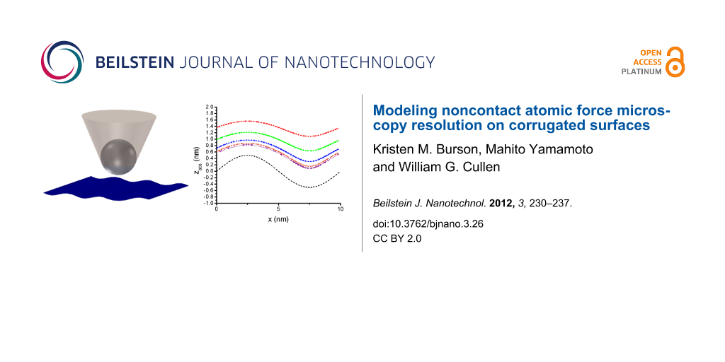
Attenuation of surface features
To determine the degree of attenuation of surface features for NC-AFM, contours of constant frequency shift were calculated (Figure 6) by using the method described in the previous section. Here, we present results for a tip with radius 5 nm. With increasing distance from the surface these contours show attenuation of the corrugation. As discussed in the previous section, the proximity to the surface is limited by our first numerical integration to obtain wa–s. At our computational limit, the nearest contour that we can calculate corresponds to a normalized frequency shift of −0.72 nN·nm1/2 (−22.8 fN·m1/2), which is well into the range in which atomic-resolution images are normally obtained [20]. Most significantly, at this interaction level the contours are attenuated by ~30% (lower-most contour, purple curve in Figure 6). At −0.1 nN·nm1/2 (upper-most contour, red curve in Figure 6) the model predicts over 50% attenuation compared to the surface corrugation. The attenuation of surface features can be understood intuitively by considering the vdW interaction of the tip and the corrugated sample surface. For flat surfaces, the vdW interaction provides a constant background and is most strongly concentrated at the tip apex, but for corrugated surfaces the vdW interactions over peak positions and valley positions are different and interactions with the side of the tip become more important. For the valley positions, the attractive force between the tip and the sides of the valley will lead to a stronger attraction than for the flat surface case and thus result in a higher z position for the same frequency shift. A similar physical argument can be made for the peak positions. In this case the downward slope means that neighboring atoms are farther away, the vdW interactions with these atoms is smaller compared with the flat case due to the increased distance, and as a result the same frequency shift will occur at a lower z position. The vdW interactions with neighboring atoms become more dominant at larger z distances (smaller frequency shifts), and therefore one can intuitively expect greater attenuation (lowering of peak positions and heightening of valley positions) based on these simple, physical vdW arguments. A similar argument was presented by Sun et. al in describing the attenuation in the graphene moiré structure on Ir(111) due to the vdW interaction between the tip and the underlying Ir(111) structure [29]. While attenuation is to be expected for increased distance between the tip and the sample, we emphasize that the degree of attenuation for a tip of 5 nm radius is significant even at small distances, with a normalized frequency shift that is relatively large. To obtain accurate experimental results with NC-AFM it is of critical importance to choose a frequency shift setpoint such that the distance between the tip and the surface is minimized, especially when seeking accurate topography of corrugated surfaces. The model used does not account for local bonding, electrostatic forces, or atomistic interactions beyond the inclusion of a pairwise vdW interaction, all of which affect the AFM resolution; nonetheless, even if these interactions were included, the varying vdW and resultant attenuation of features still presents a problem to resolution.
![[2190-4286-3-26-6]](/bjnano/content/figures/2190-4286-3-26-6.svg?scale=2.0&max-width=1024&background=FFFFFF)
Figure 6: Contours of constant normalized frequency shift, γ, for a corrugated surface. Attenuation is observed as the distance from the surface increases. Here, zabs gives an absolute position in the z direction, not a relative distance from the surface.
Figure 6: Contours of constant normalized frequency shift, γ, for a corrugated surface. Attenuation is observ...
Conclusion
As is already well known in the field of atomic force microscopy, a sharp tip and close proximity to the surface is the key to obtaining accurate topographic images with high resolution. Here we have shown that, even more so than for flat surfaces, these factors are especially important for high-resolution imaging of rough surfaces, based only on the differences between vdW interactions. While the model results support the experimental difficulty of obtaining accurate images of rough surfaces, the model itself oversimplifies the multifaceted complexities of experimental AFM setups. More complex models, which include short-range bonding and electrostatic forces, more realistic tip geometries, and calculations for closer proximities between tip and sample, are needed for a more complete and quantitatively accurate understanding of the factors limiting the resolution of corrugated surfaces.
Experimental
All NC-AFM images were collected with a JEOL ultrahigh-vacuum atomic force microscope with a base pressure of 4 × 10⁻⁸ Pa. SiO2 samples (Figure 1a and Figure 1b) were cleaved in air to the proper size then quickly transferred into the ultrahigh-vacuum JEOL AFM system (4500A, Nanonis controller). SiO2 samples were baked at 130 °C for cleaning. In order to replicate the experimental substrate preparation often used for graphene exfoliation, no additional cleaning procedures were performed before imaging of the SiO2. Si(111) samples (Figure 1c) were cleaned in UHV by the standard procedure with repeated flashing at 1530 K, followed by slow cooling through the (1 × 1)-to-(7 × 7) phase transition [30]. NC-AFM measurements were performed with commercially available cantilevers; supersharp tips were used for the high-resolution SiO2 measurements (Veeco TESP-SS with nominal radius of 2–5 nm), metal-coated Si for the under-resolved SiO2 measurements (MikroMasch DPER15), and uncoated Si for the Si(111) measurements (Nanosensors Point Probe NCH with nominal radius 7 nm). All images are presented in raw form, with only a plane-fit background subtraction. Commercial software (SPIP) was used for the presentation of image data.
Acknowledgements
The authors acknowledge Prof. Peter Grutter and Prof. Santiago Solares for very insightful discussions. This work was supported by the University of Maryland NSF-MRSEC under Grant No. DMR 05-20471. MRSEC Shared Experimental Facilities were used in this work. Additional infrastructure support provided by the UMD NanoCenter and CNAM.
References
-
Luan, B.; Robbins, M. O. Phys. Rev. E 2006, 74, 026111. doi:10.1103/PhysRevE.74.026111
Return to citation in text: [1] -
Zappone, B.; Rosenberg, K. J.; Israelachvili, J. Tribol. Lett. 2007, 26, 191. doi:10.1007/s11249-006-9172-y
Return to citation in text: [1] -
Deshpande, A.; Bao, W.; Miao, F.; Lau, C. N.; LeRoy, B. J. Phys. Rev. B 2009, 79, 205411. doi:10.1103/PhysRevB.79.205411
Return to citation in text: [1] -
Geringer, V.; Liebmann, M.; Echtermeyer, T.; Runte, S.; Schmidt, M.; Rückamp, R.; Lemme, M. C.; Morgenstern, M. Phys. Rev. Lett. 2009, 102, 076102. doi:10.1103/PhysRevLett.102.076102
Return to citation in text: [1] [2] -
Ishigami, M.; Chen, J. H.; Cullen, W. G.; Fuhrer, M. S.; Williams, E. D. Nano Lett. 2007, 7, 1643. doi:10.1021/nl070613a
Return to citation in text: [1] [2] -
Stolyarova, E.; Rim, K. T.; Ryu, S.; Maultzsch, J.; Kim, P.; Brus, L. E.; Heinz, T. F.; Hybertsen, M. S.; Flynn, G. W. Proc. Natl. Acad. Sci. U. S. A. 2007, 104, 9209. doi:10.1073/pnas.0703337104
Return to citation in text: [1] [2] -
Zhang, Y.; Brar, V. W.; Girit, C.; Zettl, A.; Crommie, M. F. Nat. Phys. 2009, 5, 722. doi:10.1038/nphys1365
Return to citation in text: [1] -
Novoselov, K. S.; Geim, A. K.; Morozov, S. V.; Jiang, D.; Zhang, Y.; Dubonos, S. V.; Grigorieva, I. V.; Firsov, A. A. Science 2004, 306, 666. doi:10.1126/science.1102896
Return to citation in text: [1] -
Meyer, J. C.; Geim, A. K.; Katsnelson, M. I.; Novoselov, K. S.; Booth, T. J.; Roth, S. Nature 2007, 446, 60. doi:10.1038/nature05545
Return to citation in text: [1] [2] -
Nelson, D. R.; Peliti, L. J. J. Phys. (Paris) 1987, 48, 1085. doi:10.1051/jphys:019870048070108500
Return to citation in text: [1] -
Aitken, Z. H.; Huang, R. J. Appl. Phys. 2010, 107, 123531. doi:10.1063/1.3437642
Return to citation in text: [1] [2] [3] [4] -
Li, T.; Zhang, Z. J. Phys. D: Appl. Phys. 2010, 43, 075303. doi:10.1088/0022-3727/43/7/075303
Return to citation in text: [1] -
Pierre-Louis, O. Phys. Rev. E 2008, 78, 021603. doi:10.1103/PhysRevE.78.021603
Return to citation in text: [1] -
Cullen, W. G.; Yamamoto, M.; Burson, K. M.; Chen, J. H.; Jang, C.; Li, L.; Fuhrer, M. S.; Williams, E. D. Phys. Rev. Lett. 2010, 105, 215504. doi:10.1103/PhysRevLett.105.215504
Return to citation in text: [1] -
Koenig, S. P.; Boddeti, N. G.; Dunn, M. L.; Bunch, J. S. Nat. Nanotechnol. 2011, 6, 543. doi:10.1038/nnano.2011.123
Return to citation in text: [1] -
Lee, C.; Li, Q.; Kalb, W.; Liu, X.-Z.; Berger, H.; Carpick, R. W.; Hone, J. Science 2010, 328, 76. doi:10.1126/science.1184167
Return to citation in text: [1] -
Raberg, W.; Wandelt, K. Appl. Phys. A: Mater. Sci. Process. 1998, 66, S1143. doi:10.1007/s003390051314
Return to citation in text: [1] -
Raberg, W.; Ostadrahimi, A. H.; Kayser, T.; Wandelt, K. J. Non-Cryst. Solids 2005, 351, 1089. doi:10.1016/j.jnoncrysol.2005.01.022
Return to citation in text: [1] [2] [3] -
Burson, K. M.; Yamamoto, M.; Cullen, W. G. High resolution microscopy of SiO2 and the structure of SiO2-supported graphene. In Proceedings of the ASME 2011 International Design Engineering Technical Conferences & Computers and Information in Engineering Conference IDETC/CIE 2011, Washington, DC, Aug 28–31, 2011; ASME: New York, 2012.
Return to citation in text: [1] -
Giessibl, F. J. Rev. Mod. Phys. 2003, 75, 949. doi:10.1103/RevModPhys.75.949
Return to citation in text: [1] [2] [3] -
Lantz, M. A.; Hug, H. J.; van Schendel, P. J. A.; Hoffmann, R.; Martin, S.; Baratoff, A.; Abdurixit, A.; Güntherodt, H.-J.; Gerber, C. Phys. Rev. Lett. 2000, 84, 2642. doi:10.1103/PhysRevLett.84.2642
Return to citation in text: [1] -
Minobe, T.; Uchihashi, T.; Tsukamoto, T.; Shigeki, O.; Sugawara, Y.; Morita, S. Appl. Surf. Sci. 1999, 140, 298. doi:10.1016/S0169-4332(98)00544-3
Return to citation in text: [1] -
Pérez, R.; Štich, I.; Payne, M. C.; Terakura, K. Phys. Rev. B 1998, 58, 10835. doi:10.1103/PhysRevB.58.10835
Return to citation in text: [1] -
Hölscher, H.; Allers, W.; Schwarz, U. D.; Schwarz, A.; Wiesendanger, R. Phys. Rev. B 2000, 62, 6967. doi:10.1103/PhysRevB.62.6967
Return to citation in text: [1] -
Israelachvili, J. N. Intermolecular And Surface Forces, 3rd ed.; Academic Press: Burlington, MA, 2011.
Return to citation in text: [1] [2] -
Hölscher, H.; Schwarz, A.; Allers, W.; Schwarz, U. D.; Wiesendanger, R. Phys. Rev. B 2000, 61, 12678. doi:10.1103/PhysRevB.61.12678
Return to citation in text: [1] -
Lantz, M. A.; Hug, H. J.; Hoffmann, R.; van Schendel, P. J. A.; Kappenberger, P.; Martin, S.; Baratoff, A.; Güntherodt, H.-J. Science 2001, 291, 2580. doi:10.1126/science.1057824
Return to citation in text: [1] -
Giessibl, F. J. Appl. Phys. Lett. 2001, 78, 123. doi:10.1063/1.1335546
Return to citation in text: [1] -
Sun, Z.; Hämäläinen, S. K.; Sainio, J.; Lahtinen, J.; Vanmaekelbergh, D.; Liljeroth, P. Phys. Rev. B 2011, 83, 081415. doi:10.1103/PhysRevB.83.081415
Return to citation in text: [1] -
Conrad, B. R.; Cullen, W. G.; Riddick, B. C.; Williams, E. D. Surf. Sci. 2009, 603, L27. doi:10.1016/j.susc.2008.12.020
Return to citation in text: [1]
| 29. | Sun, Z.; Hämäläinen, S. K.; Sainio, J.; Lahtinen, J.; Vanmaekelbergh, D.; Liljeroth, P. Phys. Rev. B 2011, 83, 081415. doi:10.1103/PhysRevB.83.081415 |
| 30. | Conrad, B. R.; Cullen, W. G.; Riddick, B. C.; Williams, E. D. Surf. Sci. 2009, 603, L27. doi:10.1016/j.susc.2008.12.020 |
| 1. | Luan, B.; Robbins, M. O. Phys. Rev. E 2006, 74, 026111. doi:10.1103/PhysRevE.74.026111 |
| 2. | Zappone, B.; Rosenberg, K. J.; Israelachvili, J. Tribol. Lett. 2007, 26, 191. doi:10.1007/s11249-006-9172-y |
| 9. | Meyer, J. C.; Geim, A. K.; Katsnelson, M. I.; Novoselov, K. S.; Booth, T. J.; Roth, S. Nature 2007, 446, 60. doi:10.1038/nature05545 |
| 18. | Raberg, W.; Ostadrahimi, A. H.; Kayser, T.; Wandelt, K. J. Non-Cryst. Solids 2005, 351, 1089. doi:10.1016/j.jnoncrysol.2005.01.022 |
| 5. | Ishigami, M.; Chen, J. H.; Cullen, W. G.; Fuhrer, M. S.; Williams, E. D. Nano Lett. 2007, 7, 1643. doi:10.1021/nl070613a |
| 6. | Stolyarova, E.; Rim, K. T.; Ryu, S.; Maultzsch, J.; Kim, P.; Brus, L. E.; Heinz, T. F.; Hybertsen, M. S.; Flynn, G. W. Proc. Natl. Acad. Sci. U. S. A. 2007, 104, 9209. doi:10.1073/pnas.0703337104 |
| 18. | Raberg, W.; Ostadrahimi, A. H.; Kayser, T.; Wandelt, K. J. Non-Cryst. Solids 2005, 351, 1089. doi:10.1016/j.jnoncrysol.2005.01.022 |
| 8. | Novoselov, K. S.; Geim, A. K.; Morozov, S. V.; Jiang, D.; Zhang, Y.; Dubonos, S. V.; Grigorieva, I. V.; Firsov, A. A. Science 2004, 306, 666. doi:10.1126/science.1102896 |
| 17. | Raberg, W.; Wandelt, K. Appl. Phys. A: Mater. Sci. Process. 1998, 66, S1143. doi:10.1007/s003390051314 |
| 3. | Deshpande, A.; Bao, W.; Miao, F.; Lau, C. N.; LeRoy, B. J. Phys. Rev. B 2009, 79, 205411. doi:10.1103/PhysRevB.79.205411 |
| 4. | Geringer, V.; Liebmann, M.; Echtermeyer, T.; Runte, S.; Schmidt, M.; Rückamp, R.; Lemme, M. C.; Morgenstern, M. Phys. Rev. Lett. 2009, 102, 076102. doi:10.1103/PhysRevLett.102.076102 |
| 5. | Ishigami, M.; Chen, J. H.; Cullen, W. G.; Fuhrer, M. S.; Williams, E. D. Nano Lett. 2007, 7, 1643. doi:10.1021/nl070613a |
| 6. | Stolyarova, E.; Rim, K. T.; Ryu, S.; Maultzsch, J.; Kim, P.; Brus, L. E.; Heinz, T. F.; Hybertsen, M. S.; Flynn, G. W. Proc. Natl. Acad. Sci. U. S. A. 2007, 104, 9209. doi:10.1073/pnas.0703337104 |
| 7. | Zhang, Y.; Brar, V. W.; Girit, C.; Zettl, A.; Crommie, M. F. Nat. Phys. 2009, 5, 722. doi:10.1038/nphys1365 |
| 18. | Raberg, W.; Ostadrahimi, A. H.; Kayser, T.; Wandelt, K. J. Non-Cryst. Solids 2005, 351, 1089. doi:10.1016/j.jnoncrysol.2005.01.022 |
| 11. | Aitken, Z. H.; Huang, R. J. Appl. Phys. 2010, 107, 123531. doi:10.1063/1.3437642 |
| 12. | Li, T.; Zhang, Z. J. Phys. D: Appl. Phys. 2010, 43, 075303. doi:10.1088/0022-3727/43/7/075303 |
| 13. | Pierre-Louis, O. Phys. Rev. E 2008, 78, 021603. doi:10.1103/PhysRevE.78.021603 |
| 15. | Koenig, S. P.; Boddeti, N. G.; Dunn, M. L.; Bunch, J. S. Nat. Nanotechnol. 2011, 6, 543. doi:10.1038/nnano.2011.123 |
| 9. | Meyer, J. C.; Geim, A. K.; Katsnelson, M. I.; Novoselov, K. S.; Booth, T. J.; Roth, S. Nature 2007, 446, 60. doi:10.1038/nature05545 |
| 16. | Lee, C.; Li, Q.; Kalb, W.; Liu, X.-Z.; Berger, H.; Carpick, R. W.; Hone, J. Science 2010, 328, 76. doi:10.1126/science.1184167 |
| 4. | Geringer, V.; Liebmann, M.; Echtermeyer, T.; Runte, S.; Schmidt, M.; Rückamp, R.; Lemme, M. C.; Morgenstern, M. Phys. Rev. Lett. 2009, 102, 076102. doi:10.1103/PhysRevLett.102.076102 |
| 10. | Nelson, D. R.; Peliti, L. J. J. Phys. (Paris) 1987, 48, 1085. doi:10.1051/jphys:019870048070108500 |
| 14. | Cullen, W. G.; Yamamoto, M.; Burson, K. M.; Chen, J. H.; Jang, C.; Li, L.; Fuhrer, M. S.; Williams, E. D. Phys. Rev. Lett. 2010, 105, 215504. doi:10.1103/PhysRevLett.105.215504 |
| 24. | Hölscher, H.; Allers, W.; Schwarz, U. D.; Schwarz, A.; Wiesendanger, R. Phys. Rev. B 2000, 62, 6967. doi:10.1103/PhysRevB.62.6967 |
| 19. | Burson, K. M.; Yamamoto, M.; Cullen, W. G. High resolution microscopy of SiO2 and the structure of SiO2-supported graphene. In Proceedings of the ASME 2011 International Design Engineering Technical Conferences & Computers and Information in Engineering Conference IDETC/CIE 2011, Washington, DC, Aug 28–31, 2011; ASME: New York, 2012. |
| 20. | Giessibl, F. J. Rev. Mod. Phys. 2003, 75, 949. doi:10.1103/RevModPhys.75.949 |
| 21. | Lantz, M. A.; Hug, H. J.; van Schendel, P. J. A.; Hoffmann, R.; Martin, S.; Baratoff, A.; Abdurixit, A.; Güntherodt, H.-J.; Gerber, C. Phys. Rev. Lett. 2000, 84, 2642. doi:10.1103/PhysRevLett.84.2642 |
| 22. | Minobe, T.; Uchihashi, T.; Tsukamoto, T.; Shigeki, O.; Sugawara, Y.; Morita, S. Appl. Surf. Sci. 1999, 140, 298. doi:10.1016/S0169-4332(98)00544-3 |
| 23. | Pérez, R.; Štich, I.; Payne, M. C.; Terakura, K. Phys. Rev. B 1998, 58, 10835. doi:10.1103/PhysRevB.58.10835 |
| 11. | Aitken, Z. H.; Huang, R. J. Appl. Phys. 2010, 107, 123531. doi:10.1063/1.3437642 |
| 11. | Aitken, Z. H.; Huang, R. J. Appl. Phys. 2010, 107, 123531. doi:10.1063/1.3437642 |
| 25. | Israelachvili, J. N. Intermolecular And Surface Forces, 3rd ed.; Academic Press: Burlington, MA, 2011. |
| 26. | Hölscher, H.; Schwarz, A.; Allers, W.; Schwarz, U. D.; Wiesendanger, R. Phys. Rev. B 2000, 61, 12678. doi:10.1103/PhysRevB.61.12678 |
| 27. | Lantz, M. A.; Hug, H. J.; Hoffmann, R.; van Schendel, P. J. A.; Kappenberger, P.; Martin, S.; Baratoff, A.; Güntherodt, H.-J. Science 2001, 291, 2580. doi:10.1126/science.1057824 |
| 11. | Aitken, Z. H.; Huang, R. J. Appl. Phys. 2010, 107, 123531. doi:10.1063/1.3437642 |
| 25. | Israelachvili, J. N. Intermolecular And Surface Forces, 3rd ed.; Academic Press: Burlington, MA, 2011. |
© 2012 Burson et al; licensee Beilstein-Institut.
This is an Open Access article under the terms of the Creative Commons Attribution License (http://creativecommons.org/licenses/by/2.0), which permits unrestricted use, distribution, and reproduction in any medium, provided the original work is properly cited.
The license is subject to the Beilstein Journal of Nanotechnology terms and conditions: (http://www.beilstein-journals.org/bjnano)