Abstract
This paper describes the atomic layer deposition of In2(S,O)3 films by using In(acac)3 (acac = acetylacetonate), H2S and either H2O or O2 plasma as oxygen sources. First, the growth of pure In2S3 films was studied in order to better understand the influence of the oxygen pulses. X-Ray diffraction measurements, optical analysis and energy dispersive X-ray spectroscopy were performed to characterize the samples. When H2O was used as the oxygen source, the films have structural and optical properties, and the atomic composition of pure In2S3. No pure In2O3 films could be grown by using H2O or O2 plasma. However, In2(S,O)3 films could be successfully grown by using O2 plasma as oxygen source at a deposition temperature of T = 160 °C, because of an exchange reaction between S and O atoms. By adjusting the number of In2O3 growth cycles in relation to the number of In2S3 growth cycles, the optical band gap of the resulting thin films could be tuned.
Introduction
Chalcopyrite-type thin film solar cells that are based on a Cu(In,Ga)Se2 (CIGS) absorber have reached high efficiencies, up to 20.3% [1] in 2011 and 20.4% [2] on flexible substrates in 2013. The best efficiencies were obtained by using cadmium sulfide (CdS) as buffer layer in solar cells with a glass/Mo/CIGS/CdS/i-ZnO/ZnO:Al stack. The buffer layer is an n-type semiconductor that forms the p–n junction with the p-type CIGS absorber, and also modifies the CIGS surface chemistry, which is usually too sensitive for a direct deposition of the window layers. However, because of the toxicity of cadmium and the low optical band gap of CdS (2.4 eV [3]) that limits the light conversion of CIGS in the UV range of the solar spectrum, alternative materials have been developed. Most Cd-free buffer layers are based on zinc and indium-compounds, with current record efficiencies obtained by chemical bath deposition (CBD, 19.7% and 19.1% for Zn(S,O,OH) [4,5], 15.7% for In(S,O,OH) [6]) or atomic layer deposition (ALD, 18.5% for Zn(O,S) [7], 18.1% for (Zn,Mg)O [8], 16.4% for In2S3 [9], and 18.2% for (Zn,Sn)O [10]). Recently, our group has synthesized new mixed films of ZnS/In2S3 by using ALD and applied them as buffer layers in CIGS solar cells [11,12]. ALD is based on sequential self-saturated reactions that allows the conformal and uniform growth of thin films with a high control of their properties [13-15]. It is therefore a suitable technique for the deposition of buffer layers. Platzer-Björkman et al. have used ALD to improve the energy-band alignment between the CIGS and the front electrode by controlling the oxygen concentration in Zn(S,O) buffer layers [4,16]. Oxygen-doping of In2S3 films is known to increase their optical band gap value [6,17,18]. Indeed, by O-doping of In2S3 films deposited by thermal evaporation, Barreau et al. could increase the optical band gap value of In2S3 thin films from 2.1 to 2.9 eV [17]. In the same way, by using the spray pyrolysis technique, Maha et al. have inserted sulfur atoms in In2O3 thin films and obtained optical band gaps in the range from 3.85 to 3.96 eV [18]. Thus, based on our previous results and those studies, we became interested in adjusting the optical properties of In2S3 by incorporating oxygen atoms while using the advantages of ALD. Typical ALD processes for the deposition of In2S3 and In2O3 are referenced in Table 1. As ALD processes of In2O3 report relatively small growth rates, we will consider the case of plasma enhancement. Indeed, plasma-enhanced ALD (PEALD), in which various reactive species are generated, has been the key for the development of fast thin-film deposition processes at low temperature. It is widely used to enhance the thin-film deposition of materials such as Al2O3, ZnO, Ta2O5, TiN, TaN and SiNx [19].
Table 1: Typical ALD processes for the deposition of In2O3 and In2S3.
| reactant A | reactant B | temperature (°C) | growth rate (Å/cycle) | reference |
|---|---|---|---|---|
| indium oxide | ||||
| InCl3 | H2O | 500 | 0.27 | [20] |
| InCp | O3/O2/H2O | 250 | 1.3/0.16/0.068 | [21] |
| InCp | H2O & O2 | 100–250 | 1.0–1.6 | [22] |
| TmIn | H2O | 217 | 0.39 | [23] |
| In(acac)3 | H2O/O3 | 165–225 | 0.2/0.12 | [24] |
| indium sulfide | ||||
| InCl3 | H2S | 300 | 1.4 | [25] |
| In(acac)3 | H2S | 160, 180, 160, 150 | 0.6, 0.7, 0.44, 0.3 | [9,26-28] |
In this study, ALD and PEALD have been used to synthesize In2(S,O)3 thin films and carry out optical band-gap engineering. The structural, optical and growth properties of the films will be studied and the role of the plasma will be discussed.
Results
Study of In(acac)3, H2S and H2O system
First, a controlled growth of pure In2S3 films was established and the film properties were measured in order to clearly identify the influence of oxygen pulse later in the study. For that, In2S3 growth was achieved in the temperature range between 140 and 240 °C. An In2S3 growth cycle consists of the following steps: In(acac)3 exposure/N2 purge/H2S exposure/N2 purge = 0.1/5/0.1/5 s, the relative long purge time being chosen to ensure a good homogeneity. Figure 1a shows the growth rate of In2S3 thin films at various temperatures. It globally increases with the temperature. An ALD window can be speculatively observed between 160 °C and 200 °C with a mean growth rate of 0.84 Å/cycle. The variation of the In2S3 growth rate with different In(acac)3 pulse lengths at a process temperature of 160 °C is illustrated in Figure 1b. This variation only slightly influences the growth rate and a saturation by lengthening the precursor pulse is not observed. The data suggest that the results displayed on Figure 1a may not have been obtained under completely self-limiting conditions. Structural and optical properties of the films were also investigated. In2S3 thin films have an amorphous structure for deposition temperatures below 180 °C and a β-tetragonal crystal structure at higher temperatures. Their indirect optical band gap varies from 2.0 eV to 2.2 eV.
![[2190-4286-4-85-1]](/bjnano/content/figures/2190-4286-4-85-1.png?scale=2.0&max-width=1024&background=FFFFFF)
Figure 1: Growth rate of pure In2S3 a) as function of the process temperature b) as function of the In(acac)3 pulse length.
Figure 1: Growth rate of pure In2S3 a) as function of the process temperature b) as function of the In(acac)3...
Then, we attempted to synthesize In2(S,O)3 film by inserting an In2O3 growth cycle. For this H2O was pulsed, instead of H2S in the growth of pure In2S3, which led to the supercycles n·{In2S3} + {In2O3} with n = 1,2,3,5,9,14,19, which correspond to ratios of {50%, 33%, 25%, 10%, 6.7%, 5%} of In2O3 cycles at a deposition temperature of 200 °C. All samples were deposited performing a total of 2000 growth cycles, i.e., 100 supercycles for n = 19, 133 supercycles for n = 14, etc. Energy dispersive X-ray spectroscopy analysis was performed on the samples and gave atomic ratios of 0.4 for In/(In+S) and 0.6 for S/(In+S), which correspond to typical In2S3 atomic ratios. The oxygen contents are similar to those of pure In2S3 films, which is assigned to the oxygen contamination of the substrate. Those results were confirmed by GI-XRD measurements. They were performed to investigate the influence of the H2O pulse on the microstructure of the films (Figure 2b). Not all samples were crystalline and the crystalline ones can be attributed to β-In2S3 with a random orientation by comparing the diffraction patterns with the reference data and with the literature [27]. Indeed, we should observe a peak shift due to increasing oxygen doping when changing the In2O3/In2S3 ratio. However, the peaks remain at the same diffraction angles. Comparing the FWHM of the (109) peak, the maximum FWHM measured was 1.2° for the 10%-In2O3 sample, which corresponds to the thickest film. In general it can be said that the thinner the films, the lower the FWHM. From these observations, it seems that we obtained In2S3 films only.
![[2190-4286-4-85-2]](/bjnano/content/figures/2190-4286-4-85-2.png?scale=2.0&max-width=1024&background=FFFFFF)
Figure 2: Influence of the number of In2O3 cycles on (a) the growth rate while using H2O as oxygen precursor and (b) GIXRD diffractogram. The reference diffraction pattern for In2S3 is taken from the database JCPDS 00-005-0731.
Figure 2: Influence of the number of In2O3 cycles on (a) the growth rate while using H2O as oxygen precursor ...
Thin films optical absorption were determined from transmittance (T) and reflectance (R) measurements by using the following formula [29]
![[Graphic 1]](/bjnano/content/inline/2190-4286-4-85-i5.svg?max-width=637&scale=1.18182)
where α is the absorption coefficient and t is the film thickness. Figure 3 shows absorption spectra of the thin films. They are presented in the form of (α)0.5 = f(E), which is linear for indirect band gap materials and allows for the determination of the optical transition. The optical band gaps correspond to an indirect transition in the range from 1.9 to 2.2 eV, which is roughly similar to that of pure In2S3 film optical properties. No correlation could be found between either the ratio of In2O3 cycles or the film thickness and the optical measurements. These results are in accordance with the observations of the structural analysis. Consequently, this method is not suitable to synthesize In2(S,O)3 thin films. In parallel, we attempted to synthesize pure In2O3 films from In(acac)3 and H2O at temperatures of 160 and 200 °C. This remained unsuccessful, because no films could be grown under these conditions.
![[2190-4286-4-85-3]](/bjnano/content/figures/2190-4286-4-85-3.png?scale=2.0&max-width=1024&background=FFFFFF)
Figure 3: Influence of the ratio of In2O3 cycles on the film absorption spectra when using H2O as oxygen precursor.
Figure 3: Influence of the ratio of In2O3 cycles on the film absorption spectra when using H2O as oxygen prec...
Study of the In(acac)3, H2S and O2 plasma system
As O2 plasma is known to have a different reactivity, it was evaluated as potential oxygen source for the deposition of In2(S,O)3. Thin film syntheses were performed by incorporating In2O3 growth cycles that use O2 plasma pulses in the growth of In2S3: In(acac)3 exposure/N2 purge/O2 + plasma exposure/N2 purge = 0.1/5/7/3 s in the following supercycles n·{In2S3} + 2·{In2O3} with n = 15,20,25,30,35,40 which correspond to ratios of {11.8%, 9.1%, 7.4%, 6.25%, 5.4%, 4.8%} of In2O3 cycles at a deposition temperature of 160 °C. A total of 2000 cycles was achieved for all samples as described in the previous section. The dependence of the growth rate on the number of In2O3 cycles is shown in Figure 4a. When increasing the ratio from 4.8% to 9.1%, the growth rate increases up to 1.4 Å/cycle and then decreases again. The variation of the film thickness with the number of ALD cycles for a ratio of 10% of In2O3 cycles is illustrated in Figure 4b. A linear growth is observed up to 1500 ALD cycles. GIXRD measurements revealed an amorphous structure in all the samples.
![[2190-4286-4-85-4]](/bjnano/content/figures/2190-4286-4-85-4.png?scale=2.0&max-width=1024&background=FFFFFF)
Figure 4: Influence of a) the number of In2O3 cycles on the growth rate b) the number of process cycles on the film thickness when using O2 plasma as oxygen precursor. The dotted line is a guide to the eyes.
Figure 4: Influence of a) the number of In2O3 cycles on the growth rate b) the number of process cycles on th...
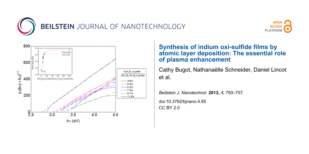
Transmittance and reflectance measurements were carried out on the In2(S,O)3 samples. Figure 5 shows the transmittance of In2(S,O)3 films as a function of the percentage of In2O3 cycles. A shift of the onset absorption can be observed, which suggests an evolution in the properties of the films. The indirect optical transitions were identified for all samples from their respective absorption spectra (Figure 6a). The values are plotted as a function of the ratio of In2O3 cycles in Figure 6b. The maximum value corresponds to the theoretical optical gap of In2O3 [30]. The optical band gaps vary from 2.2 ± 0.1 eV for pure In2S3 to 3.3 ± 0.1 eV for In2(S,O)3 and increase with the number of In2O3 cycles during the deposition process of In2S3.
![[2190-4286-4-85-5]](/bjnano/content/figures/2190-4286-4-85-5.png?scale=2.0&max-width=1024&background=FFFFFF)
Figure 5: Influence of the number of In2O3 cycle on the film transmittance when using O2 plasma as oxygen precursor.
Figure 5: Influence of the number of In2O3 cycle on the film transmittance when using O2 plasma as oxygen pre...
![[2190-4286-4-85-6]](/bjnano/content/figures/2190-4286-4-85-6.png?scale=2.0&max-width=1024&background=FFFFFF)
Figure 6: Influence of the number of In2O3 cycles a) on the absorption and b) optical band gap when using O2 plasma as oxygen precursor. The dotted line is a guide to the eyes.
Figure 6: Influence of the number of In2O3 cycles a) on the absorption and b) optical band gap when using O2 ...
The atomic ratios of oxygen, sulfur and indium determined by using EDX are presented in Table 2 and correlated to the optical band gap values. The dependence of the atomic ratio of oxygen and the optical band gap on the number of In2O3 cycles is not clear. In general, high oxygen concentrations of more than 66 atom % were measured in the films.
Table 2: EDX measurements data from In2(S,O)3 thin films when using O2 plasma.
|
In2O3
(%) |
optical band gap
(eV) |
(O+S)/(In+S+O)
(atom %) |
In/(In+S+O)
(atom %) |
S/(In+S+O)
(atom %) |
O/(In+S+O)
(atom %) |
|---|---|---|---|---|---|
| 4.80 | 2.76 | 83 | 17 | 15 | 68 |
| 5.41 | 3.04 | 85 | 15 | 10 | 75 |
| 6.25 | 3.10 | 85 | 15 | 11 | 74 |
| 7.41 | 3.00 | 80 | 20 | 14 | 66 |
| 9.09 | 3.22 | 79 | 21 | 10 | 69 |
| 11.76 | 3.31 | 83 | 17 | 9 | 74 |
We also tried to synthesize In2(S,O)3 by using a single O2 plasma pulse instead of In2O3 pulse cycles. The following cycle program was used: 20·{In2S3} + 2·{O2+plasma exposure}/N2 purge with the same process parameters. This corresponds to 9.1% of indium cycles, which can be compared to the previous deposition with a pulse of In(acac)3 before the O2 plasma exposure. Table 3 shows the properties of these two samples, along with those of pure In2S3. Even without the In(acac)3 pulse, O and S atomic ratios indicate that the synthesized film corresponds to a In2(S,O)3 film and no significant differences were observed between the samples.
Table 3: Comparison between In2(S,O)3 films, synthesized with and without In(acac)3 during the oxidation pulse, and In2S3.
| program | Eg (eV) | growth rate (Å/cycle) | In/(In+S+O) (atom %) | S/(S+O) (atom %) | O/(S+O) (atom %) |
|---|---|---|---|---|---|
| 20·{In2S3} + 2·{In2O3} | 3.2 ± 0.1 | 1.4 ± 0.2 | 21 | 13 | 87 |
| 20·{In2S3} + 2·O2 plasma | 3.3 ± 0.1 | 1.2 ± 0.2 | 17 | 15 | 85 |
| In2S3 | 2.2 ± 0.2 | 0.7 ± 0.08 | 35 | 70 | 30 |
The growth of In2(S,O)3 growth could be achieved when using O2 plasma as oxygen precursor. The maximum growth rate was 1.4 Å/cycle, which is higher than the growth rates of In2S3 shown in Figure 1 and those reported in the literature for this deposition temperature [9,26-28]. Optical measurements revealed an onset absorption moving to higher energies when increasing the number of In2O3 cycles. At the same time, the optical band gap increased from 2.2 eV to 3.3 eV for In2O3 cycle ratios in the range from 0 to 11.8%. EDX analysis showed that those films have a high oxygen content. Finally, all attempts to synthesize pure In2O3 films from In(acac)3 and O2 plasma remained unsuccessful .
Discussion
It has been observed that inserting an In2O3 cycle during the deposition of In2S3 when using H2O as oxygen precursor has no influence on the oxygen content and on the film properties. It only affects the growth rate as the thickness varies. Attempts to synthesize pure In2O3 thin films were also unsuccessful, which suggests a low reactivity of H2O towards In(acac)3. Several authors reported the difficulty to synthesize In2O3 by ALD using β-diketonates (In(acac)3, In(hfac = hexafluoropentadionate)3, In(thd = 2,2,6,6-tetramethyl-3,5-heptanedioneate)) and water [20,21,25]. In most cases, they assigned the low growth rates or the absence of grown films to the low reactivity of water toward β-diketonates.
As no pure In2O3 films could be grown in our case, the synthesis of mixed films by a simple addition of two layers, i.e., In2O3 + In2S3, is not possible. However, the deposition of ternary materials can also occur via exchange reactions. For instance, when synthesizing zinc indium sulfide (ZIS) thin films, substitution mechanisms between diethylzinc (DEZ) and In2S3 could be demonstrated [11]. Similar mechanisms also occur when inserting H2O in pure ZnS during the growth of Zn(S,O) by using ALD [4,16]. Such processes do not seem to occur in our case, because the In2(S,O)3 deposition method that uses H2O remained unsuccessful. A possible thermodynamic explanation for the unfavorable deposition of In2(S,O)3 using H2O as oxygen precursor is that the following exchange reaction is endothermic and thus unlikely to occur [31].
![[2190-4286-4-85-i1]](/bjnano/content/inline/2190-4286-4-85-i1.svg?max-width=590&scale=1.18182)
Due to the high reactivity of radicals, PEALD generally allows the achievement of many chemical reactions that cannot occur with thermal ALD [13,19]. Here In2(S,O)3 films could be grown while using O2 plasma as oxygen source. But the growth of pure In2O3 films remained unsuccessful. This suggests that the oxygen contained in In2(S,O)3 films is not generated from single layers of In2O3 but rather by exchange reactions as described in the previous section. Indeed, the O2 plasma can directly react with the film surface and induce an exchange reaction with surface sulfur atoms. Figure 7 presents a scheme of the assumed substitution mechanism at the surface.
![[2190-4286-4-85-7]](/bjnano/content/figures/2190-4286-4-85-7.png?scale=2.0&max-width=1024&background=FFFFFF)
Figure 7: Surface mechanisms during the O2 plasma pulse.
Figure 7: Surface mechanisms during the O2 plasma pulse.
The following exchange reactions can explain the substitution of S atoms by reactive oxygen species generated in the plasma. Indeed, their free standard enthalpies all have negative values:
![[2190-4286-4-85-i2]](/bjnano/content/inline/2190-4286-4-85-i2.svg?max-width=590&scale=1.18182)
![[2190-4286-4-85-i3]](/bjnano/content/inline/2190-4286-4-85-i3.svg?max-width=590&scale=1.18182)
![[2190-4286-4-85-i4]](/bjnano/content/inline/2190-4286-4-85-i4.svg?max-width=590&scale=1.18182)
Thus, when comparing these reactions with the reaction between In2S3 and H2O, it seems that the doping is only favorable when using O2 plasma as oxygen precursor, because these reactions are all exothermic. This thermochemical analysis and the observation that In2(O,S)3 films obtained from the two different ALD pulse programs 20·{In2S3} + 2·{In2O3} and 20·{In2S3} + 2·O2 plasma have similar properties, show the critical role of activated oxygen during the deposition of In2(S,O)3.
Commonly existing species in oxygen plasmas are atomic oxygen that is created from molecular oxygen dissociation, excited oxygen species at different electronic levels, ionized oxygen or recombined species like O3 [32,33]. Consequently, exchange reactions between adsorbed oxygen and oxygen species from the gas phase or recombination reactions have to be considered. Marinov et al. studied the interactions between a radiofrequency O2 plasma and oxide surfaces like TiO2, SiO2 and Pyrex [32]. They demonstrated that these materials surfaces are continuously re-structured under O2 plasma exposure because of the exchange reactions that occur between O atoms in the films and oxygen species of the gas phase. They also reported that reaction products undergo oxidation at the surface and assumed that two surface mechanisms could occur; O + O → O2 and O + O2 → O3. Such mechanisms might also occur in our case considering the exchange reactions described in Figure 7 during the first O2 plasma pulse. Indeed, no match was found between the ratios of In2O3 cycles during the deposition of In2(S,O)3 films and the oxygen content of the films determined by EDX. When the number of In2O3 cycles varied from 4.8% to 11.8%, in the same time the oxygen content of the films varied from 68 atom % to 75 atom %. Oxidation mechanisms during deposition process can explain these high differences between the expected values and those measured.
Comparing In2(S,O)3 films synthesized with and without an In(acac)3 pulse before the O2 plasma pulse, no significant differences in the band gap values or the atomic ratios of the samples were observed. This confirms that the formation of an In2O3 single layer is not required to synthesize In2(S,O)3 films. These results are in fair agreement with the fact that the growth of pure In2O3 remained unsuccessful. Thus, we can assume that only activated oxygen is involved during the deposition of In2(S,O)3, and In2S3 can be considered as an intermediate state for the formation of In2(S,O)3.
On-going studies focus on a better understanding on the nature of the oxygen species generated by the plasma, their role in oxidizing mechanisms and the reason of the relatively low indium content. One of them could be an excessive adsorption of oxygen in the film and the formation of sulfates. Further studies, in particular by using X-ray photoelectron spectroscopy, are in progress to assess the presence or not of such groups. Experiments will also be performed to study the influence of other oxygen sources such as O2 alone and O3.
Conclusion
In this study we reported the atomic layer deposition of In2(S,O)3 films by using In(acac)3 (acac = acetylacetonate), H2S, and either H2O or O2 plasma as oxygen sources. In2(S,O)3 films could only be obtained with O2 plasma as oxygen source, and all attempts to synthesize In2O3 remained unsuccessful. Thus, synthesis of In2(S,O)3 films is likely to occur through an exchange reaction instead of simple mixing of In2S3 and In2O3 layers. A thermochemical analysis can explain such observations. Indeed, this reaction is endothermic for H2O and exothermic for O2 plasma.
With this new synthesis method, the optical band gap of the thin films could be tuned from 2.2 eV to 3.3 eV by increasing the number of O2 plasma pulses. The high oxygen contents measured in the films (>66 atom %) in comparison to the initial number of In2O3 pulses might be explained by the fact that oxidation mechanisms occurred on the film surfaces during the O2 plasma pulses. Due to the reactivity of the plasma, the film surfaces cannot be considered as a static system but should rather be seen as continually re-structured surfaces. In our future studies, those films will be applied as buffer layer in Cu(In,Ga)Se2 solar cells to investigate their suitability as Cd-free buffer layer for thin film solar cells.
Experimental
In2S3 and In2(S,O)3 thin films were deposited on borosilicate glass and Si(100) substrates in a SUNALE R-200 ALD reactor (Picosun Oy.) with a modified 15 cm × 15 cm square reaction chamber. All samples were deposited performing a total of 2000 growth cycles. The source material for indium was indium acetylacetonate (In(CH3COCHCOCH3)3), In(acac)3, (98%, Strem Chemicals). Hydrogen sulfide, H2S (99.5%, Messer) was used as the sulfur source. Deionized Millipore vapor water and O2, (99.9995%, Messer) were used as oxygen source. O2 was introduced in a remote RF plasma generator with Argon (99.9997%, Messer) as carrier gas, and the plasma power was kept at 2600 W. All sources were kept at room temperature while In(acac)3 was heated to 200 °C. The carrying and purge gas was nitrogen with a purity of 99.9999% (Messer). The pressure in the reaction chamber was kept in the range from 1 to 4 mbar.
The thickness of the films was measured using a VEECO DEKTAK 6M profilometer on glass substrates. Thicknesses were determined after creating steps in the films, by masking film parts with chemically resistant tape and dipping the film in nitric acid (45% in water) at room temperature for 60 s. The uncertainty given for the thickness is the standard deviation of six measurements taking into account the uncertainty of the profilometer, the sharpness of steps, the film roughness, and the film inhomogeneity. Transmittance and reflectance spectra were obtained by using a PerkinElmer lambda 900 Spectrophotometer with a PELA-1000 integrating sphere. All optical measurements were performed on borosilicate glass substrates. X-Ray diffraction (XRD) studies were performed under grazing incidence X-ray diffraction conditions with a PANalytical Empyrean diffractometer while using Cu Kα radiation. X-Ray reflectometry analyses were also performed to confirm thickness measurements. Thin film compositions were obtained by using a Magellan 400L scanning electron microscope provided by FEI. It is equipped with an energy dispersive X-ray spectroscopy detector INCASynergy 350. All EDX measurements were carried out on Si(100) substrates and the values reported are atomic percentages (atom %).
References
-
Jackson, P.; Hariskos, D.; Lotter, E.; Paetel, S.; Wuerz, R.; Menner, R.; Wischmann, W.; Powalla, M. Prog. Photovoltaics 2011, 19, 894–897. doi:10.1002/pip.1078
Return to citation in text: [1] -
Empa – CIGS. http://www.empa.ch/plugin/template/empa/*/79143 (accessed July 31, 2013).
Return to citation in text: [1] -
Çetinörgü, E.; Gümüş, C.; Esen, R. Thin Solid Films 2006, 515, 1688–1693. doi:10.1016/j.tsf.2006.06.004
Return to citation in text: [1] -
Nakamura, M.; Kouji, Y.; Chiba, Y.; Hakuma, H.; Kobayashi, T.; Nakada, T. Achievement of 19.7% efficiency with a small-sized Cu(InGa)(SeS)2 solar cells prepared by sulfurization after selenizaion process with Zn-based buffer. 38th IEEE Photovoltaic Specialists Conference, June 3–8, 2012; Austin, TX.
Return to citation in text: [1] [2] [3] -
Hariskos, D.; Menner, R.; Jackson, P.; Paetel, S.; Witte, W.; Wischmann, W.; Powalla, M.; Bürkert, L.; Kolb, T.; Oertel, M.; Dimmler, B.; Fuchs, B. Prog. Photovoltaics 2012, 20, 534–542. doi:10.1002/pip.1244
Return to citation in text: [1] -
Hariskos, D.; Ruckh, M.; Rühle, U.; Walter, T.; Schock, H. W.; Hedström, J.; Stolt, L. Sol. Energy Mater. Sol. Cells 1996, 41–42, 345–353. doi:10.1016/0927-0248(96)80009-2
Return to citation in text: [1] [2] -
Zimmermann, U.; Ruth, M.; Edoff, M. In 21st European Photovoltaic Solar Energy Conference: Proceedings of the international conference held in Dresden, Dresden, Germany, Sept 4–8, 2006; pp 1831–1834.
Return to citation in text: [1] -
Platzer-Björkman, C.; Hultqvist, A.; Pettersson, J.; Törndahl, T. Proc. SPIE 2010, 7603, 76030F. doi:10.1117/12.846017
Return to citation in text: [1] -
Naghavi, N.; Spiering, S.; Powalla, M.; Cavana, B.; Lincot, D. Prog. Photovoltaics 2003, 11, 437–443. doi:10.1002/pip.508
Return to citation in text: [1] [2] [3] -
Lindahl, J.; Zimmermann, U.; Szaniawski, P.; Torndahl, T.; Hultqvist, A.; Salome, P.; Platzer-Bjorkman, C.; Edoff, M. IEEE J. Photovoltaics 2013, 3, 1100–1105. doi:10.1109/JPHOTOV.2013.2256232
Return to citation in text: [1] -
Genevée, P.; Donsanti, F.; Renou, G.; Lincot, D. J. Phys. Chem. C 2011, 115, 17197–17205. doi:10.1021/jp203604j
Return to citation in text: [1] [2] -
Genevée, P.; Donsanti, F.; Renou, G.; Lincot, D. Atomic Layer Deposition of ZnInxSy Buffer Layers For Copper Indium Gallium Diselenide Thin Film Solar Cells. In 26th European Photovoltaic Solar Energy Conference and Exhibition: EU PVSEC Proceedings, Hamburg, Germany, Sept 5–8, 2011; pp 2428–2431. doi:10.4229/26thEUPVSEC2011-3CO.4.4
Return to citation in text: [1] -
Miikkulainen, V.; Leskela, M.; Ritala, M.; Puurunen, R. L. J. Appl. Phys. 2013, 113, 021301. doi:10.1063/1.4757907
Return to citation in text: [1] [2] -
van Delft, J. A.; Garcia-Alonso, D.; Kessels, W. M. M. Semicond. Sci. Technol. 2012, 27, 074002. doi:10.1088/0268-1242/27/7/074002
Return to citation in text: [1] -
Bakke, J. R.; Pickrahn, K. L.; Brennan, T. P.; Bent, S. F. Nanoscale 2011, 3, 3482–3508. doi:10.1039/c1nr10349k
Return to citation in text: [1] -
Platzer-Björkman, C.; Törndahl, T.; Abou-Ras, D.; Malmström, J.; Kessler, J.; Stolt, L. J. Appl. Phys. 2006, 100, 044506. doi:10.1063/1.2222067
Return to citation in text: [1] [2] -
Barreau, N.; Marsillac, S.; Albertini, D.; Bernede, J. C. Thin Solid Films 2002, 403–404, 331–334. doi:10.1016/S0040-6090(01)01512-7
Return to citation in text: [1] [2] -
Maha, M. H. Z.; Bagheri-Mohagheghi, M.-M.; Azimi-Juybari, H.; Shokooh-Saremi, M. Phys. Scr. 2012, 86, 055701. doi:10.1088/0031-8949/86/05/055701
Return to citation in text: [1] [2] -
Kim, H. Thin Solid Films 2011, 519, 6639–6644. doi:10.1016/j.tsf.2011.01.404
Return to citation in text: [1] [2] -
Asikainen, T.; Ritala, M.; Leskelä, M. J. Electrochem. Soc. 1994, 141, 3210–3213. doi:10.1149/1.2059303
Return to citation in text: [1] [2] -
Elam, J. W.; Martinson, A. B. F.; Pellin, M. J.; Hupp, J. T. Chem. Mater. 2006, 18, 3571–3578. doi:10.1021/cm060754y
Return to citation in text: [1] [2] -
Elam, J. W.; Libera, J. A.; Hryn, J. N. ECS Trans. 2011, 41, 147–155. doi:10.1149/1.3633663
Return to citation in text: [1] -
Lee, D.-J.; Kwon, J.-Y.; Lee, J. I.; Kim, K.-B. J. Phys. Chem. C 2011, 115, 15384–15389. doi:10.1021/jp2024389
Return to citation in text: [1] -
Nilsen, O.; Balasundaraprabhu, R.; Monakhov, E. V.; Muthukumarasamy, N.; Fjellvåg, H.; Svensson, B. G. Thin Solid Films 2009, 517, 6320–6322. doi:10.1016/j.tsf.2009.02.059
Return to citation in text: [1] -
Asikainen, T.; Ritala, M.; Leskelä, M. Appl. Surf. Sci. 1994, 82–83, 122–125. doi:10.1016/0169-4332(94)90206-2
Return to citation in text: [1] [2] -
Yousfi, E. B.; Weinberger, B.; Donsanti, F.; Cowache, P.; Lincot, D. Thin Solid Films 2001, 387, 29–32. doi:10.1016/S0040-6090(00)01838-1
Return to citation in text: [1] [2] -
Sterner, J.; Malmström, J.; Stolt, L. Prog. Photovoltaics 2005, 13, 179–193. doi:10.1002/pip.595
Return to citation in text: [1] [2] [3] -
Sarkar, S. K.; Kim, J. Y.; Goldstein, D. N.; Neale, N. R.; Zhu, K.; Elliott, C. M.; Frank, A. J.; George, S. M. J. Phys. Chem. C 2010, 114, 8032–8039. doi:10.1021/jp9086943
Return to citation in text: [1] [2] -
Hishikawa, Y.; Nakamura, N.; Tsuda, S.; Nakano, S.; Kishi, Y.; Kuwano, Y. Jpn. J. Appl. Phys. 1991, 30, 1008–1014. doi:10.1143/JJAP.30.1008
Return to citation in text: [1] -
Liu, D.; Lei, W. W.; Zou, B.; Yu, S. D.; Hao, J.; Wang, K.; Liu, B. B.; Cui, Q. L.; Zou, G. T. J. Appl. Phys. 2008, 104, 083506. doi:10.1063/1.2999369
Return to citation in text: [1] -
HSC Chemistry; Chemistry Software Ltd, 2013.
Return to citation in text: [1] -
Marinov, D. Adsorption réactive des molécules et radicaux sur des surfaces sous exposition plasma. Ph.D. Thesis, Ecole Polytechnique X, Palaiseau, France, 2012.
Return to citation in text: [1] [2] -
Lopaev, D. V.; Malykhin, E. M.; Zyryanov, S. M. J. Phys. D: Appl. Phys. 2011, 44, 015202. doi:10.1088/0022-3727/44/1/015202
Return to citation in text: [1]
| 20. | Asikainen, T.; Ritala, M.; Leskelä, M. J. Electrochem. Soc. 1994, 141, 3210–3213. doi:10.1149/1.2059303 |
| 21. | Elam, J. W.; Martinson, A. B. F.; Pellin, M. J.; Hupp, J. T. Chem. Mater. 2006, 18, 3571–3578. doi:10.1021/cm060754y |
| 25. | Asikainen, T.; Ritala, M.; Leskelä, M. Appl. Surf. Sci. 1994, 82–83, 122–125. doi:10.1016/0169-4332(94)90206-2 |
| 11. | Genevée, P.; Donsanti, F.; Renou, G.; Lincot, D. J. Phys. Chem. C 2011, 115, 17197–17205. doi:10.1021/jp203604j |
| 4. | Nakamura, M.; Kouji, Y.; Chiba, Y.; Hakuma, H.; Kobayashi, T.; Nakada, T. Achievement of 19.7% efficiency with a small-sized Cu(InGa)(SeS)2 solar cells prepared by sulfurization after selenizaion process with Zn-based buffer. 38th IEEE Photovoltaic Specialists Conference, June 3–8, 2012; Austin, TX. |
| 16. | Platzer-Björkman, C.; Törndahl, T.; Abou-Ras, D.; Malmström, J.; Kessler, J.; Stolt, L. J. Appl. Phys. 2006, 100, 044506. doi:10.1063/1.2222067 |
| 1. | Jackson, P.; Hariskos, D.; Lotter, E.; Paetel, S.; Wuerz, R.; Menner, R.; Wischmann, W.; Powalla, M. Prog. Photovoltaics 2011, 19, 894–897. doi:10.1002/pip.1078 |
| 6. | Hariskos, D.; Ruckh, M.; Rühle, U.; Walter, T.; Schock, H. W.; Hedström, J.; Stolt, L. Sol. Energy Mater. Sol. Cells 1996, 41–42, 345–353. doi:10.1016/0927-0248(96)80009-2 |
| 18. | Maha, M. H. Z.; Bagheri-Mohagheghi, M.-M.; Azimi-Juybari, H.; Shokooh-Saremi, M. Phys. Scr. 2012, 86, 055701. doi:10.1088/0031-8949/86/05/055701 |
| 4. | Nakamura, M.; Kouji, Y.; Chiba, Y.; Hakuma, H.; Kobayashi, T.; Nakada, T. Achievement of 19.7% efficiency with a small-sized Cu(InGa)(SeS)2 solar cells prepared by sulfurization after selenizaion process with Zn-based buffer. 38th IEEE Photovoltaic Specialists Conference, June 3–8, 2012; Austin, TX. |
| 5. | Hariskos, D.; Menner, R.; Jackson, P.; Paetel, S.; Witte, W.; Wischmann, W.; Powalla, M.; Bürkert, L.; Kolb, T.; Oertel, M.; Dimmler, B.; Fuchs, B. Prog. Photovoltaics 2012, 20, 534–542. doi:10.1002/pip.1244 |
| 3. | Çetinörgü, E.; Gümüş, C.; Esen, R. Thin Solid Films 2006, 515, 1688–1693. doi:10.1016/j.tsf.2006.06.004 |
| 6. | Hariskos, D.; Ruckh, M.; Rühle, U.; Walter, T.; Schock, H. W.; Hedström, J.; Stolt, L. Sol. Energy Mater. Sol. Cells 1996, 41–42, 345–353. doi:10.1016/0927-0248(96)80009-2 |
| 17. | Barreau, N.; Marsillac, S.; Albertini, D.; Bernede, J. C. Thin Solid Films 2002, 403–404, 331–334. doi:10.1016/S0040-6090(01)01512-7 |
| 18. | Maha, M. H. Z.; Bagheri-Mohagheghi, M.-M.; Azimi-Juybari, H.; Shokooh-Saremi, M. Phys. Scr. 2012, 86, 055701. doi:10.1088/0031-8949/86/05/055701 |
| 2. | Empa – CIGS. http://www.empa.ch/plugin/template/empa/*/79143 (accessed July 31, 2013). |
| 17. | Barreau, N.; Marsillac, S.; Albertini, D.; Bernede, J. C. Thin Solid Films 2002, 403–404, 331–334. doi:10.1016/S0040-6090(01)01512-7 |
| 10. | Lindahl, J.; Zimmermann, U.; Szaniawski, P.; Torndahl, T.; Hultqvist, A.; Salome, P.; Platzer-Bjorkman, C.; Edoff, M. IEEE J. Photovoltaics 2013, 3, 1100–1105. doi:10.1109/JPHOTOV.2013.2256232 |
| 13. | Miikkulainen, V.; Leskela, M.; Ritala, M.; Puurunen, R. L. J. Appl. Phys. 2013, 113, 021301. doi:10.1063/1.4757907 |
| 14. | van Delft, J. A.; Garcia-Alonso, D.; Kessels, W. M. M. Semicond. Sci. Technol. 2012, 27, 074002. doi:10.1088/0268-1242/27/7/074002 |
| 15. | Bakke, J. R.; Pickrahn, K. L.; Brennan, T. P.; Bent, S. F. Nanoscale 2011, 3, 3482–3508. doi:10.1039/c1nr10349k |
| 32. | Marinov, D. Adsorption réactive des molécules et radicaux sur des surfaces sous exposition plasma. Ph.D. Thesis, Ecole Polytechnique X, Palaiseau, France, 2012. |
| 33. | Lopaev, D. V.; Malykhin, E. M.; Zyryanov, S. M. J. Phys. D: Appl. Phys. 2011, 44, 015202. doi:10.1088/0022-3727/44/1/015202 |
| 9. | Naghavi, N.; Spiering, S.; Powalla, M.; Cavana, B.; Lincot, D. Prog. Photovoltaics 2003, 11, 437–443. doi:10.1002/pip.508 |
| 4. | Nakamura, M.; Kouji, Y.; Chiba, Y.; Hakuma, H.; Kobayashi, T.; Nakada, T. Achievement of 19.7% efficiency with a small-sized Cu(InGa)(SeS)2 solar cells prepared by sulfurization after selenizaion process with Zn-based buffer. 38th IEEE Photovoltaic Specialists Conference, June 3–8, 2012; Austin, TX. |
| 16. | Platzer-Björkman, C.; Törndahl, T.; Abou-Ras, D.; Malmström, J.; Kessler, J.; Stolt, L. J. Appl. Phys. 2006, 100, 044506. doi:10.1063/1.2222067 |
| 32. | Marinov, D. Adsorption réactive des molécules et radicaux sur des surfaces sous exposition plasma. Ph.D. Thesis, Ecole Polytechnique X, Palaiseau, France, 2012. |
| 8. | Platzer-Björkman, C.; Hultqvist, A.; Pettersson, J.; Törndahl, T. Proc. SPIE 2010, 7603, 76030F. doi:10.1117/12.846017 |
| 7. | Zimmermann, U.; Ruth, M.; Edoff, M. In 21st European Photovoltaic Solar Energy Conference: Proceedings of the international conference held in Dresden, Dresden, Germany, Sept 4–8, 2006; pp 1831–1834. |
| 11. | Genevée, P.; Donsanti, F.; Renou, G.; Lincot, D. J. Phys. Chem. C 2011, 115, 17197–17205. doi:10.1021/jp203604j |
| 12. | Genevée, P.; Donsanti, F.; Renou, G.; Lincot, D. Atomic Layer Deposition of ZnInxSy Buffer Layers For Copper Indium Gallium Diselenide Thin Film Solar Cells. In 26th European Photovoltaic Solar Energy Conference and Exhibition: EU PVSEC Proceedings, Hamburg, Germany, Sept 5–8, 2011; pp 2428–2431. doi:10.4229/26thEUPVSEC2011-3CO.4.4 |
| 13. | Miikkulainen, V.; Leskela, M.; Ritala, M.; Puurunen, R. L. J. Appl. Phys. 2013, 113, 021301. doi:10.1063/1.4757907 |
| 19. | Kim, H. Thin Solid Films 2011, 519, 6639–6644. doi:10.1016/j.tsf.2011.01.404 |
| 22. | Elam, J. W.; Libera, J. A.; Hryn, J. N. ECS Trans. 2011, 41, 147–155. doi:10.1149/1.3633663 |
| 20. | Asikainen, T.; Ritala, M.; Leskelä, M. J. Electrochem. Soc. 1994, 141, 3210–3213. doi:10.1149/1.2059303 |
| 21. | Elam, J. W.; Martinson, A. B. F.; Pellin, M. J.; Hupp, J. T. Chem. Mater. 2006, 18, 3571–3578. doi:10.1021/cm060754y |
| 30. | Liu, D.; Lei, W. W.; Zou, B.; Yu, S. D.; Hao, J.; Wang, K.; Liu, B. B.; Cui, Q. L.; Zou, G. T. J. Appl. Phys. 2008, 104, 083506. doi:10.1063/1.2999369 |
| 9. | Naghavi, N.; Spiering, S.; Powalla, M.; Cavana, B.; Lincot, D. Prog. Photovoltaics 2003, 11, 437–443. doi:10.1002/pip.508 |
| 26. | Yousfi, E. B.; Weinberger, B.; Donsanti, F.; Cowache, P.; Lincot, D. Thin Solid Films 2001, 387, 29–32. doi:10.1016/S0040-6090(00)01838-1 |
| 27. | Sterner, J.; Malmström, J.; Stolt, L. Prog. Photovoltaics 2005, 13, 179–193. doi:10.1002/pip.595 |
| 28. | Sarkar, S. K.; Kim, J. Y.; Goldstein, D. N.; Neale, N. R.; Zhu, K.; Elliott, C. M.; Frank, A. J.; George, S. M. J. Phys. Chem. C 2010, 114, 8032–8039. doi:10.1021/jp9086943 |
| 27. | Sterner, J.; Malmström, J.; Stolt, L. Prog. Photovoltaics 2005, 13, 179–193. doi:10.1002/pip.595 |
| 29. | Hishikawa, Y.; Nakamura, N.; Tsuda, S.; Nakano, S.; Kishi, Y.; Kuwano, Y. Jpn. J. Appl. Phys. 1991, 30, 1008–1014. doi:10.1143/JJAP.30.1008 |
| 25. | Asikainen, T.; Ritala, M.; Leskelä, M. Appl. Surf. Sci. 1994, 82–83, 122–125. doi:10.1016/0169-4332(94)90206-2 |
| 9. | Naghavi, N.; Spiering, S.; Powalla, M.; Cavana, B.; Lincot, D. Prog. Photovoltaics 2003, 11, 437–443. doi:10.1002/pip.508 |
| 26. | Yousfi, E. B.; Weinberger, B.; Donsanti, F.; Cowache, P.; Lincot, D. Thin Solid Films 2001, 387, 29–32. doi:10.1016/S0040-6090(00)01838-1 |
| 27. | Sterner, J.; Malmström, J.; Stolt, L. Prog. Photovoltaics 2005, 13, 179–193. doi:10.1002/pip.595 |
| 28. | Sarkar, S. K.; Kim, J. Y.; Goldstein, D. N.; Neale, N. R.; Zhu, K.; Elliott, C. M.; Frank, A. J.; George, S. M. J. Phys. Chem. C 2010, 114, 8032–8039. doi:10.1021/jp9086943 |
| 23. | Lee, D.-J.; Kwon, J.-Y.; Lee, J. I.; Kim, K.-B. J. Phys. Chem. C 2011, 115, 15384–15389. doi:10.1021/jp2024389 |
| 24. | Nilsen, O.; Balasundaraprabhu, R.; Monakhov, E. V.; Muthukumarasamy, N.; Fjellvåg, H.; Svensson, B. G. Thin Solid Films 2009, 517, 6320–6322. doi:10.1016/j.tsf.2009.02.059 |
© 2013 Bugot et al; licensee Beilstein-Institut.
This is an Open Access article under the terms of the Creative Commons Attribution License (http://creativecommons.org/licenses/by/2.0), which permits unrestricted use, distribution, and reproduction in any medium, provided the original work is properly cited.
The license is subject to the Beilstein Journal of Nanotechnology terms and conditions: (http://www.beilstein-journals.org/bjnano)